HYSTERETIC NOISE IN DC SQUIDS
- 格式:pdf
- 大小:280.70 KB
- 文档页数:4

噪音对海洋影响英语作文Title: The Impact of Noise Pollution on the Ocean。
The ocean, a vast expanse of water covering over 70% of our planet, is not as silent as one might think. In recent years, the issue of noise pollution in the ocean has gained increasing attention. This essay explores the various sources of oceanic noise pollution and its profound impact on marine life and ecosystems.To begin with, let us delve into the primary sources of noise pollution in the ocean. One major source is anthropogenic activities, including shipping, industrial operations, and naval exercises. The incessant hum of ship engines, the deafening blasts of underwater construction, and the sonar pings of military vessels all contribute to the cacophony beneath the waves. Additionally, offshore drilling and seismic surveys for oil and gas exploration emit intense bursts of noise, disrupting the marine environment.Furthermore, marine life itself can generatesignificant noise, particularly from marine mammals such as whales and dolphins. These creatures rely on sound for communication, navigation, and hunting. However, their vocalizations can be drowned out by human-generated noise, leading to communication breakdowns and behavioral changes.Now, let us explore the profound impact of noise pollution on marine life and ecosystems. The most evident effect is on marine mammals, whose sensitive hearing is vital for survival. Prolonged exposure to high-intensity noise can result in auditory damage, disorientation, and even strandings. Whales, in particular, have been known to alter their migration routes and feeding behaviors to avoid noisy areas.Moreover, noise pollution can disrupt the natural balance of marine ecosystems. For instance, certain fish species rely on sound for mating calls and territorial defense. Excessive noise can interfere with these crucial behaviors, leading to decreased reproductive success andpopulation decline. Additionally, noise can mask the sounds of prey and predators, affecting the dynamics of marinefood webs.Furthermore, noise pollution poses a significant threat to sensitive marine habitats, such as coral reefs and seagrass meadows. These ecosystems provide essential breeding grounds and nurseries for countless marine species. However, the relentless din of human activities can stress corals, impairing their growth and resilience. Similarly, noise can disturb the delicate equilibrium of seagrass ecosystems, affecting the abundance and diversity of associated marine life.In conclusion, noise pollution is a pervasive and detrimental threat to the health of the ocean and its inhabitants. From the rumble of ships to the roar ofoffshore drilling, human-generated noise permeates every corner of the marine environment. Its impacts are far-reaching, affecting marine mammals, fish, and delicate ecosystems alike. To mitigate the effects of noise pollution, concerted efforts are needed, including stricterregulations, technological innovations, and public awareness campaigns. Only by reducing our noise footprint can we ensure the tranquility and well-being of the ocean for generations to come.。

第44卷第3期航天返回与遥感2023年6月SPACECRAFT RECOVERY & REMOTE SENSING79红外影像奇偶元条纹噪声自适应去除算法李岩(北京空间机电研究所,北京100094)摘要由于工艺原因,TDI型红外探测器的光敏元均为交错分布,奇偶元响应输出均是基于不同的通道,这样导致某些TDI红外探测器图像上一些位置仍残留有奇偶元条纹噪声,该噪声不仅影响目视效果,也影响后续的定量应用。
文章针对该奇偶元条纹噪声提出一种自适应的条纹噪声去除算法,此方法不仅可以自适应地检测出奇偶元条纹噪声并进行去除,也可以对闪元噪声进行有效检测及去除;最后,基于在轨图像进行了算法的验证,试验结果表明该算法可以有效的去除奇偶元条纹噪声。
关键词红外探测器自适应奇偶元条纹噪声去除中图分类号: X87文献标志码: A 文章编号: 1009-8518(2023)03-0079-06DOI: 10.3969/j.issn.1009-8518.2023.03.009An Adaptive Algorithm for Eliminating Odd-Even Stripe Noise inInfrared ImageLI Yan(Beijing Institute of Space Mechanics & Electricity, Beijing 100094, China)Abstract The elements of the TDI array infrared detector are staggered distribution because of the technical reason. The output of odd and even elements is from different channels. Odd-even stripe noise was found in some images because of the odd-even output from different channels. The odd-even stripe noise not only affects the visual effect, but also affects the quantitative application. A new adaptive algorithm was proposed to eliminate the odd-even stripe noise. This algorithm could detect and remove the odd-even stripe noise adaptively. It also could detect and remove the flash noise effectively. Finally, the algorithm is verified based on the on-orbit image, and the experimental results show that the algorithm can effectively remove the odd-even stripe noise.Keywords infrared detector; adaptive algorithm; odd and even elements; stripe noise removal0 引言时间延迟积分(TDI)型红外探测器作为第二代红外探测器,具有更高的空间分辨率和温度灵敏度。
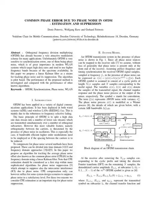
COMMON PHASE ERROR DUE TO PHASE NOISE IN OFDM-ESTIMATION AND SUPPRESSIONDenis Petrovic,Wolfgang Rave and Gerhard FettweisV odafone Chair for Mobile Communications,Dresden University of Technology,Helmholtzstrasse18,Dresden,Germany{petrovic,rave,fettweis}@ifn.et.tu-dresden.deAbstract-Orthogonal frequency division multiplexing (OFDM)has already become a very attractive modulation scheme for many applications.Unfortunately OFDM is very sensitive to synchronization errors,one of them being phase noise,which is of great importance in modern WLAN systems which target high data rates and tend to use higher frequency bands because of the spectrum availability.In this paper we propose a linear Kalmanfilter as a means for tracking phase noise and its suppression.The algorithm is pilot based.The performance of the proposed method is investigated and compared with the performance of other known algorithms.Keywords-OFDM,Synchronization,Phase noise,WLANI.I NTRODUCTIONOFDM has been applied in a variety of digital commu-nications applications.It has been deployed in both wired systems(xDSL)and wireless LANs(IEEE802.11a).This is mainly due to the robustness to frequency selective fading. The basic principle of OFDM is to split a high data rate data stream into a number of lower rate streams which are transmitted simultaneously over a number of orthogonal subcarriers.However this most valuable feature,namely orthogonality between the carriers,is threatened by the presence of phase noise in oscillators.This is especially the case,if bandwidth efficient higher order modulations need to be employed or if the spacing between the carriers is to be reduced.To compensate for phase noise several methods have been proposed.These can be divided into time domain[1][2]and frequency domain approaches[3][4][5].In this paper we propose an algorithm for tracking the average phase noise offset also known as the common phase error(CPE)[6]in the frequency domain using a linear Kalmanfilter.Note that CPE estimation should be considered as afirst step within more sophisticated algorithms for phase noise suppression[5] which attempt to suppress also the intercarrier interference (ICI)due to phase noise.CPE compensation only,can however suffice for some system design scenarios to suppress phase noise to a satisfactory level.For these two reasons we consider CPE estimation as an important step for phase noise suppression.II.S YSTEM M ODELAn OFDM transmission system in the presence of phase noise is shown in Fig. 1.Since all phase noise sources can be mapped to the receiver side[7]we assume,without loss of generality that phase noise is present only at the front end of the receiver.Assuming perfect frequency and timing synchronization the received OFDM signal samples, sampled at frequency f s,in the presence of phase noise can be expressed as r(n)=(x(n) h(n))e jφ(n)+ξ(n).Each OFDM symbol is assumed to consist of a cyclic prefix of length N CP samples and N samples corresponding to the useful signal.The variables x(n),h(n)andφ(n)denote the samples of the transmitted signal,the channel impulse response and the phase noise process at the output of the mixer,respectively.The symbol stands for convolution. The termξ(n)represents AWGN noise with varianceσ2n. The phase noise processφ(t)is modelled as a Wiener process[8],the details of which are given below,with a certain3dB bandwidth∆f3dB.,0,1,2...m lX l=,0,1,2...m lR l=Fig.1Block diagram of an OFDM transmission chain.At the receiver after removing the N CP samples cor-responding to the cyclic prefix and taking the discrete Fourier transform(DFT)on the remaining N samples,the demodulated carrier amplitude R m,lkat subcarrier l k(l k= 0,1,...N−1)of the m th OFDM symbol is given as[4]:R m,lk=X m,lkH m,lkI m(0)+ζm,lk+ηm,lk(1)where X m,lk,H m,lkandηm,lkrepresent the transmitted symbol on subcarrier l k,the channel transfer function andlinearly transformed AWGN with unchanged variance σ2n at subcarrier l k ,respectively.The term ζm,l k represents intercarrier interference (ICI)due to phase noise and was shown to be a gaussian distributed,zero mean,randomvariable with variance σ2ICI =πN ∆f 3dB s[7].The term I m (0)also stems from phase noise.It does not depend on the subcarrier index and modifies all subcarriers of one OFDM symbol in the same manner.As its modulus is in addition very close to one [9],it can be seen as a symbol rotation in the complex plane.Thus it is referred to in the literature as the common phase error (CPE)[6].The constellation rotation due to CPE causes unaccept-able system performance [7].Acceptable performance can be achieved if one estimates I m (0)or its argument and compensates the effect of the CPE by derotating the received subcarrier symbols in the frequency domain (see Eq.(1)),which significantly reduces the error rate as compared to the case where no compensation is used.The problem of esti-mating the CPE was addressed by several authors [3][4][10].In [3]the authors concentrated on estimating the argument of I m (0)using a simple averaging over pilots.In [10]the argument of I m (0)was estimated using an extended Kalman filter,while in [4]the coefficient I m (0)itself was estimated using the LS algorithm.Here we introduce an alternative way for minimum mean square estimation (MMSE)[11]of I m (0)using a linear scalar Kalman filter.The algorithm is as [4]pilot based.III.P HASE N OISE M ODELFor our purposes we need to consider a discretized phase noise model φ(n )=φ(nT s )where n ∈N 0and T s =1/f s is the sampling period at the front end of the receiver.We adopt a Brownian motion model of the phase noise [8].The samples of the phase noise process are given as φ(n )=2πf c √cB (n )where f c is the carrier frequency,c =∆f 3dB /πf 2c [8]and B (n )represents the discretizied Brownian motion process,Using properties of the Brownian motion [12]the fol-lowing holds:B (0)=0and B (n +1)=B (n )+dB n ,n ∈N 0where each increment dB n is an independent random variable and dB n ∼√T s N (0,1).Noting that φ(n )=2πf c √cB (n )we can write the discrete time phase noise process equation asφ(n +1)=φ(n )+w (n )(2)where w (n )∼N (0,4π2f 2c cT s )is a gaussian randomvariable with zero mean and variance σ2w =4π2f 2c cT s .IV.CPE E STIMATION U SING A K ALMAN F ILTER Since all received subcarriers within one OFDM symbolare affected by the same factor,namely I m (0),the problem at hand can be seen as an example of estimating a constant from several noisy measurements given by Eq.(1)for which purpose a Kalman filter is well suited [11].For a Kalmanfilter to be used we need to define the state space model of the system.Define first the set L ={l 1,l 2,l 3,...l P }as a subset of the subcarrier set {0,1,...N −1}.Using Eq.(1)one can writeR m,l k =A m,l k I m,l k (0)+εm,l k(3)where A m,l k =X m,l k H m,l k and I m,l k (0)=I m (0)for all k =1,2...,P .Additional indexing of the CPE terms is done here only for convenience of notation.On the other hand one can writeI m,l k +1(0)=I m,l k (0).(4)Equations (3)and (4)are the measurement and processequation of the system state space model,where A m,l k represents the measurement matrix,while the process matrix is equal to 1and I m,l k (0)corresponds to the state of the system.The measuring noise is given by εm,l k which combines the ICI and AWGN terms in Eq.(1),the varianceof which for all l k equals σ2ε=(σ2ICI +σ2n ).The process noise equals zero.Note that the defined state space model is valid only for one OFDM symbol.For the state space model to be fully defined,knowledge of the A m,l k =X m,l k H m,l k is needed.Here we assume to have ideal knowledge of the channel.On the other hand we define the subset L to correspond to the pilot subcarrier locations within one OFDM symbol so that X m,q ,q ∈L are also known.We assume that at the beginning of each burst perfect timing and frequency synchronization is achieved,so that the phase error at the beginning of the burst equals zero.After the burst reception and demodulation,the demodulated symbols are one by one passed to the Kalman filter.For a Kalman filter initialization one needs for eachOFDM symbol an a priori value for ˆI m,l 1(0)and an a priori error variance K −m,1.At the beginning of the burst,when m =1,it is reasonable to adopt ˆI −1,l 1(0)=1.Within each OFDM symbol,say m th,the filter uses P received pilot subcarriers to recursively update the a priori value ˆI −1m,l 1(0).After all P pilot subcarriers are taken into account ˆI m,l P (0)is obtained,which is adopted as an estimate ofthe CPE within one OFDM symbol,denoted as ˆIm (0).The Kalman filter also provides an error variance of the estimateof I m,l P (0)as K m,P .ˆI m,l P(0)and K m,P are then used as a priori measures for the next OFDM symbol.The detailed structure of the algorithm is as follows.Step 1:InitializationˆI −m,l 1(0)=E {I −m,l 1(0)}=ˆI m −1(0)K −m,1=E {|I m (0)−ˆIm −1(0)|2}∼=E {|φm −ˆφm −1|2}=σ2CP E +K m −1,Pwhere σ2CP E =4π2N 2+13N +N CP ∆f 3dBf s(see [10]),K 0,P =0and φm =arg {I m (0)}.Repeat Step2and Step3for k=1,2,...,P Step2:a-posteriori estimation(update)G m,k=K−m,kH H m,lkH m,lkK−m,kH Hm,l k+(σ2ICI+σ2n)ˆIm,l k (0)=ˆI−m,l k(0)+G m,k[R m,lk−H m,l kˆI−m,l k(0)]K m,k=(1−G m,k H m,lk )K−m,kStep3:State and error variance propagationK−m,k+1=K m,k(5)ˆI−m,l k+1(0)=ˆI m,lk(0)Note that no matrix inversions are required,since the state space model is purely scalar.V.CPE C ORRECTIONThe easiest approach for CPE correction is to derotate all subcarriers l k of the received m th symbol R m,lkby φm=−arg{ˆI m(0)}.Unambiguity of the arg{·}function plays here no role since any unambiguity which is a multiple of2πrotates the constellation to its equivalent position in terms of its argument.The presented Kalmanfilter estimation algorithm is read-ily applicable for the decision feedback(DF)type of algo-rithm presented in[4].The idea there was to use the data symbols demodulated after thefirst CPE correction in a DFE manner to improve the quality of the estimate since that is increasing the number of observations of the quantity we want to estimate.In our case that would mean that after thefirst CPE correction the set L={l1,l2,l3,...l P}of the subcarriers used for CPE estimation,which previously corresponded to pilot subcarriers,is now extended to a larger set corresponding to all or some of the demodulated symbols. In this paper we have extended the set to all demodulated symbols.The Kalmanfilter estimation is then applied in an unchanged form for a larger set L.VI.N UMERICAL R ESULTSThe performance of the proposed algorithm is investigated and compared with the proposal of[4]which is shown to outperform other known approaches.The system model is according to the IEEE802.11a standard,where64-QAM modulation is used.We investigate the performance in AWGN channels and frequency selective channels using as an example the ETSI HiperLAN A-Channel(ETSI A). Transmission of10OFDM symbols per burst is assumed.A.Properties of an EstimatorThe quality of an estimation is investigated in terms of the mean square error(MSE)of the estimator for a range of phase noise bandwidths∆f3dB∈[10÷800]Hz.Table1 can be used to relate the phase noise bandwidth with other quantities.Figures2and3compare the MSE of the LS estimator from[4]and our approach for two channel types and both standard correction and using decision feedback. Note that SNRs are chosen such that the BER of a coded system after the Viterbi algorithm in case of phase noise free transmission is around1·10−4.Kalmanfilter shows better performance in all cases and seems to be more effective for small phase noise bandwidths. As expected when DF is used the MSE of an estimator is smaller because we are taking more measurements into account.Fig.2MSE of an estimator for AWGN channel.Fig.3MSE of an estimator for ETSI A channel.Table 1Useful relationsQuantitySymbolRelationTypical values for IEEE802.11aOscillator constant c [1radHz]8.2·10−19÷4.7·10−18Oscillator 3dB bandwidth ∆f 3dB [Hz]∆f 3dB =πf 2cc 70÷400Relative 3dB bandwidth ∆f 3dB ∆f car∆f 3dBfsN 2·10−4÷13·10−4Phase noise energy E PN [rad]E PN =4π∆f 3dB∆fcar0.0028÷0.016Subcarrier spacing∆f car∆f car =f s N312500HzB.Symbol Error Rate DegradationSymbol error rate (SER)degradation due to phase noise is investigated also for a range of phase noise bandwidths ∆f 3dB ∈[10÷800]Hz and compared for different correc-tion algorithms.Ideal CPE correction corresponds to the case when genie CPE values are available.In all cases simpleconstellation derotation with φ=−arg {ˆIm (0)}is used.Fig.4SER degradation for AWGN channel.In Figs.4and 5SER degradation for AWGN and ETSI A channels is plotted,respectively.It is interesting to note that as opposed to the ETSI A channel case in AWGN channel there is a gap between the ideal CPE and both correction approaches.This can be explained if we go back to Eq.(1)where we have seen that phase noise affects the constellation as additive noise.Estimation error of phase noise affects the constellation also in an additive manner.On the other hand the SER curve without phase noise in the AWGN case is much steeper than the corresponding one for the ETSI A channel.A small SNR degradation due to estimation errors will cause therefore large SER variations.This explains why the performance differs much less in the ETSI A channel case.Generally from this discussion a conclusion can be drawn that systems with large order of diversity are more sensitive to CPE estimation errors.Note that this ismeantFig.5SER degradation for ETSI A channel.not in terms of frequency diversity but the SER vs.SNR having closely exponential dependence.It can be seen that our approach shows slightly better performance than [4]especially for small phase noise bandwidths.What is also interesting to note is,that DF is not necessary in the case of ETSI A types of channels (small slope of SER vs.SNR)while in case of AWGN (large slope)it brings performance improvement.VII.C ONCLUSIONSWe investigated the application of a linear Kalman filter as a means for tracking phase noise and its suppression.The proposed algorithm is of low complexity and its performance was studied in terms of the mean square error (MSE)of an estimator and SER degradation.The performance of an algorithm is compared with other algorithms showing equivalent and in some cases better performance.R EFERENCES[1]R.A.Casas,S.Biracree,and A.Youtz,“Time DomainPhase Noise Correction for OFDM Signals,”IEEE Trans.on Broadcasting ,vol.48,no.3,2002.[2]M.S.El-Tanany,Y.Wu,and L.Hazy,“Analytical Mod-eling and Simulation of Phase Noise Interference in OFDM-based Digital Television Terrestial Broadcast-ing Systems,”IEEE Trans.on Broadcasting,vol.47, no.3,2001.[3]P.Robertson and S.Kaiser,“Analysis of the effects ofphase noise in OFDM systems,”in Proc.ICC,1995.[4]S.Wu and Y.Bar-Ness,“A Phase Noise SuppressionAlgorithm for OFDM-Based WLANs,”IEEE Commu-nications Letters,vol.44,May1998.[5]D.Petrovic,W.Rave,and G.Fettweis,“Phase NoiseSuppression in OFDM including Intercarrier Interfer-ence,”in Proc.Intl.OFDM Workshop(InOWo)03, pp.219–224,2003.[6]A.Armada,“Understanding the Effects of PhaseNoise in Orthogonal Frequency Division Multiplexing (OFDM),”IEEE Trans.on Broadcasting,vol.47,no.2, 2001.[7]E.Costa and S.Pupolin,“M-QAM-OFDM SystemPerformance in the Presence of a Nonlinear Amplifier and Phase Noise,”IEEE mun.,vol.50, no.3,2002.[8]A.Demir,A.Mehrotra,and J.Roychowdhury,“PhaseNoise in Oscillators:A Unifying Theory and Numerical Methods for Characterisation,”IEEE Trans.Circuits Syst.I,vol.47,May2000.[9]S.Wu and Y.Bar-ness,“Performance Analysis of theEffect of Phase Noise in OFDM Systems,”in IEEE 7th ISSSTA,2002.[10]D.Petrovic,W.Rave,and G.Fettweis,“Phase NoiseSuppression in OFDM using a Kalman Filter,”in Proc.WPMC,2003.[11]S.M.Kay,Fundamentals of Statistical Signal Process-ing vol.1.Prentice-Hall,1998.[12]D.J.Higham,“An Algorithmic Introduction to Numer-ical Simulation of Stochastic Differential Equations,”SIAM Review,vol.43,no.3,pp.525–546,2001.。
2008 Received February 12, 2007; accepted November 30, 2007; published online June 25, 2008doi: 10.1007/s11432-008-0082-5†Corresponding author (email: yunguihun@ )Supported by the National Natural Science Foundation of China (Grant No. 60372022) and Program for New Century Excellent Talents in Uni-versity (Grant No. NCET-05-0806)Sci China Ser F-Inf Sci | Oct. 2008 | vol. 51 | no. 10 | 1585-1593 eigenstructure-based methods, such as 2-D MUSIC-type method [1] and 2-D ESPRIT-type ESPRIT method is a special case of DOA matrix method [5].Unfortunately, there are also many phenomena in signal processing which are decidedly non-Gaussian [6―13], such as atmospheric noise, urban radio channels, man-made signals, and so on. Recently, it has been shown that impulsive noise can be modeled as a complex symmetric α-stable(S αS) process. Since S αS does not possess finite variance when 2α<, minimum dis-persion criterion is a good choice to evaluate the S αS process. Lv et al.[6,7] have proposed several methods using cross-covariation matrix to estimate 2-D DOAs of the signals in the presence of impulsive noise.In some applications, useful information can be obtained by introducing time domain process-ing [8,9,14―16]. He et al.[8,9] presented a DOA estimation method in impulsive noise environments using fractional lower-order spatio-temporal (FLOST) matrix. Jin [15,16] proposed a spatio-tempo- ral DOA matrix (ST-DOA) algorithm which takes advantages of the a priori in time domain. How- ever, not only 2-D ESPRIT method [2,6], but also DOA matrix method [4,5,7] and ST-DOA matrix method [15,16] cannot estimate signals with common 1-D angles or in some curved plane, which degrades the estimation performance of those algorithms.In this paper, we proposed a novel joint diagonalization FLOST matrix method (JD-FLOM- ST-DOA). The method can obtain the 2-D DOAs of the array based on joint diagonalization di-rectly with neither peak searching nor pair matching. Moreover, compared with ST-DOA matrix method, the significances of the novel algorithms are as follows: 1) it can work in impulsive noise environments; 2) it can estimate signals with common 1-D angles in any plane. Simulation results show the effectiveness of the proposed method.2 Complex S αS random variables [11]A complex random variable is S αS if and are joint S αS, and then their characteristic function is written as1j X X X =+2⎤1X 2X (1)122*11221122,12(){exp[j ()]}{exp[j()]}exp ||d (,),X X S E X E X X x x x x αϕωωωωωωΓ=+⎡=−+⎢⎥⎣⎦∫R where 12,j ωωω=+ is the real part operator, and is a symmetric measure on theunit sphere , called the spectral measure of the random variable The characteristic expo-nent is restricted to the values []i R 12,X X Γ2S .X 02,α<≤ and it determines the shape of the distribution. The smaller the characteristic exponent α, the heavier the tails of the density.A complex random variable 1j 2X X X =+ is isotropic if and only if hasa uniform spectral measure. In this case, the characteristic function of X can be written as12(,)X X (2)*(){exp[j ()]}exp(||),E X αϕωωγω==−R where (0)γγ> is the dispersion of the distribution. The dispersion plays a role analogous to the role that the variance plays for the second-order processes. Namely, it determines the spread of the probability density function around the origin. A method for generating complex isotropic S αS random variables is given in ref. [11]. Several in-phase components of the time series with different characteristic exponents are given in Figure 1, which shows the impulsiveness of the S αS distribution.1586 XIA TieQi et al. Sci China Ser F-Inf Sci | Oct. 2008 | vol. 51 | no. 10 | 1585-1593Figure 1 Time series of S αS random variables.A complex isotropic S αS random variable X has finite fractional lower-order moments (FLOMs) 2,p α<≤ i.e., {||},p E X <∞ 2.p α∀<≤ Obviously, S αS signals are of infinite variance because their second-order moments are infinite. The FLOM between ξ and η is defined as in ref. [10]:12*[,]{}{||},12,p p f E E p ξηξηξηηα−−==<<≤ (3) where, 1*||,p p ηηη−= and the superscript * denotes complex conjugate.3 Array configuration and signal model3.1 Assumptions and data modelConsider a uniform linear array consisting of M -element as shown in Figure 2. The spacing be-tween the first M −1 sensors is d x while the spacing between the first and the M th sensor is d y . Assume that there are D narrowband independent signals () (1,2,,)k s t k D =… with common carrier impinging on the array from 2-D directions (,).k k θβ As made in refs. [8,9], we assume the signal vector s (t ) satisfying2T H 1{s()[(|s()|)s ()]}diag[(),,()],p D E t t t τρτρτ−+= … (4) where superscript H denotes complex conjugate transpose, denotes Hadamard product (ele-ment-by-element product), and diag[]⋅ is the diagonal matrix formed with the elements of its vector valued argument. Eq. (4) means that the signals () (1,2,,)k s t k D =… are mutuallyFLOST uncorrelated. denotes the auto-FLOST moment of2*()[()|()|()]p k k k k E s t s t s t ρττ−=+().k s t The baseband signals of the t th snapshot of the array output measured by the array can be expressed asXIA TieQi et al. Sci China Ser F-Inf Sci | Oct. 2008 | vol. 51 | no. 10 | 1585-1593 158712π()()exp j (1)cos()(), 1,,1,Di k x k i k x t s t i d n t i M θλ=⎡⎤=−+=⎢⎥⎣⎦∑…− (5) 12π()()exp j cos()().D M k y k M k x t s t d n βλ=⎡⎤=⎢⎥⎣⎦∑t +(6)Figure 2 Array configuration for independent 2-D DOAs estimation.Write eqs. (5) and (6) into matrix form, and we have()()(),t t =+x As n t T D(7)T T 111[(),,()], ()[(),,()], [(),,()],M M x t x t t n t n t s t s t ===......x n s T 11[,,,,], [,,,,],k D k k ik Mk a a a ==............A a a a a (8)2πexp j (1)cos(), 1,,1,ik x k a i d i θλ⎡⎤M =−=⎢⎥⎣⎦…− (9) 2πexp j cos(),Mk y k a d βλ⎡⎤=⎢⎥⎣⎦(10) where is additive uniform complex isotropic S αS noise with dispersion γ, independent of the signals, i.e.,()(1,2,...,)i n t i M = 2T H {()[(|()|)()]}(),p M E t t t τ−+ n n n I γδτ= (11) where ()δτ is Kronecker function, and M I is an M M × dimensional identity matrix.3.2 FLOM-ST-DOA matrix method Under the above assumptions, we have the following array outputs of FLOST moments:2**1()[(),()][()|()|()][()],(1,2,,,0,,,,,,i M k k p x x i M f i M M D),s s Mk ik s s s s k R x t x t E x t x t x t R a a i M NT T T NT ττττττ−==+=+==≠=−−∑ (12)where 2*()[(),()][()|()|()].k k p s s k k f k k kR s t s t E s t s t s t τττ−=+=+ 2****1()[(),()][()|()|()][()], (0,1,2,,,1,2,,,1).i l k k p x x i l f i l l Dlks s Mk ik k Mk R x t x t E x t x t x t a R a a i M l L L M a τττττ−==+=+=≠==∑……=− (13)1588 XIA TieQi et al. Sci China Ser F-Inf Sci | Oct. 2008 | vol. 51 | no. 10 | 1585-1593Let (),X τR ()l Y R τ and (),S τR respectively, be1T ()[(),,(),,()],M i M M M X x x x x x x R R R ττττ=……R (14)1T ()[(),,(),,()],l l i l M l Y x x x x x x R R R ττττ=……R (15)11**1()[(),,(),,()].k k D D S s s M s s Mk s s MD R a R a R a ττττ=⋅⋅⋅……R *T (16)Write eqs. (12) and (13) into matrix form,()(),X S ττ=R AR (17)()(),l Y l S ττ=R A R Φ (18) where is a D ×D dimensional matrix,l Φ 11***1***1j2π/[cos (1)cos ]j2π/[cos (1)cos ]j2π/[cos (1)cos ]j2π/[cos (1)cos ]1diag ,,,,diag{e ,,e ,, e ,,e }diag[,,,,x y x p y p x q y q x D y D l lk lD l M Mk MD d d l d d l d d l d d l l gl a a a a a a λβθλβθλβθλβθφφ−−−−−−−−⎡⎤=⎢⎥⎣⎦==………………Φ,,], 1.ql Dl g q D φφ≠...≤≤ (19)By collecting the “pseudo snapshots” at 2N lags ,,,,,,s s s s NT T T NT τ=−−…… the “pseudo snapshots” data matrices are formed as follows:[(),,(),(),,()],X s X s X s X s NT T T NT =−−……X R R R R[(),,(),(),,()],l l l l l Y s Y s Y s Y s NT T T NT =−−……Y R R R R[(),,(),(),,()].S s S s S s S s NT T T NT =−−……S R R R R Then, eqs. (17) and (18) can be rewritten into,=X AS (20). (21) l l =Y A S ΦDefine FLOM-ST-DOA matrix as(22) †[],l TS l =⋅R Y X where denotes pseudoinverse, i.e.,†[]X†H H [][].1−=X X XX (23)Theorem 1. FLOM-ST-DOA matrix algorithm: if A and S is nonsingular and has un-equal elements, then the FLOM-ST-DOA matrix has its D non-zero eigenvalues equal to the D diagonal elements of and the corresponding eigenvectors equal to the D column vec-tors of matrix A , i.e.,l Φl TS R l Φ.l TS l =R A A Φ (24)The proof is similar to that given in ref. [5]. By eigendecomposition, we have A and . Then, the l Φk θ’s are obtained using the first M −1 elements of according to eq. (9), while (1)k D ≤≤k a k β’s are given by the M th element of according to eq. (10). The above theorem means that an estimate can be obtained if and only if there exists a matrix , which has (1)k D ≤≤k a l Φ XIA TieQi et al. Sci China Ser F-Inf Sci | Oct. 2008 | vol. 51 | no. 10 | 1585-1593 1589unequal entries. However, it is easy to construct examples where each l Φ(1)l L ≤≤ has a de-generate eigenvalue spectrum, and then the FLOM-ST-DOA matrix algorithm will fail. In the next section, we will propose an improved robust JD-FLOM-ST-DOA matrix algorithm to over-come this problem.4 JD-FLOM-ST-DOA matrix mehtod4.1 WhiteningThe first step of our JD-FLOM-ST-DOA matrix algorithm procedure consists of whitening the signal part of the pseudo-observation. This is achieved by applying a whitening matrix W to them, i.e., an ()X s nT R M D × matrix verifying the following:H H H H H [()()]X s X s X E nT nT .==WR R W WQ W WAA W I =,, (25)where and we assume thatH [()()]X X s X s E nT nT =Q R R H[()()](1/2)S S E N ττ=R R H ,0()()N S s S s n N n nT nT =−≠=∑R R Iand ()S τR has unit variance so that the dynamic range of ()S τR is accounted for by the mag-nitude of the corresponding column of A , which does not affect the estimation of the 2-D DOAs. Eq. (25) shows that if W is a whitening matrix, then is a WA D D × dimensional unitary ma-trix. It follows that for any whitening matrix W , there exists a unitary matrix U such that . As a consequence, matrix A can be factored as=WA U (26) †.=A W U Note that this whitening procedure reduces the determination of the M D × dimensional mixture matrix A to that of a unitary D D × dimensional matrix U . The whitened process still obeys a linear model:(27) ()(),X X n =z WR n n H H ..}, (28) ()().l l Y Y n =z WR Define the following cross-correlation matrix between and()l Y n z (),X n z (29)H H H H H [()()][()()][()()]l l l Y X Y X Y X l S S l E n n E n n E ττ====G z z WR R W WA R R A W U U ΦΦ4.2 Determining the unitary factor UThe second step of our JD-FLOM-STDOA matrix algorithm procedure is to determine a unitary factor U , which is obtained by performing a joint diagonalization of the combined set of The essential uniqueness of joint diagonalization is guaranteed by Theorem 2.1{,,,,}l L Y X Y X Y X= ……G G G G Theorem 2. Essential uniqueness of joint diagonalization: let be a set of L matrices where, for matrix is in the form withU a uni- tary matrix. Any joint diagonalizer of is essentially equal (the definition is given in ref. 1{,,,,l L Y X Y X Y X= ……G G G G 1l L ≤≤l Y X G H l U U Φ G [14]) 1590 XIA TieQi et al. Sci China Ser F-Inf Sci | Oct. 2008 | vol. 51 | no. 10 | 1585-1593to U if and only if1, , 1, pl ql p q D l l L .φφ∀≠∃≠≤≤≤≤ (30)The essential uniqueness condition (30) is of course much weaker than the requirement thatthere should exist a matrix in which is uniquely unitarily diagonalizable. In particular, it is easy to construct examples, where each matrix in has a degenerate eigenvalue spectrum but such that the joint diagonalizer of is nonetheless essentially unique. The proof of Theorem 2 is similar to the proof given in ref. G GG [14].Theorem 3. Sufficiency condition: if then (,)[0,π)[0,π),k k αβ∈×, 1,l l L ∃≤≤1∀≤. ,p q D ≠≤pl ql φφ≠Proof. If for the DOAs of the g th source (,)[0,π)[0,π),k k αβ∈×(,)g g αβ and q th source (,),q q αβ ,g q ≠ there exist two cases:1) if ,p q ββ≠ then 11;p q φφ≠2) if ,p q ββ=,p q αα≠ then ,pl ql φφ≠2l L ≤≤.Theorem 3 means that there exists at least one matrix satisfies (1)l l L ≤≤Φ.gl ql φφ≠Then, matrix A can be obtained by eq. (26) and the 2-D DOAs can be estimated according to eqs.(9) and (10).4.3 Implementation of the JD-FLOM-ST-DOA matrix methodBased on the previous sections, we can introduce a 2-D DOAs estimation method based on FLOST processing. The JD-FLOM-ST-DOA matrix method is defined by the following imple-mentation:1) Estimate the FLOM-ST matrix of the array outputs according to eqs. (13) and (14).2) Form the new pseudo-observation vectors X and .l Y 3) Estimate the sample covariance from the X Q 2M N × pseudo-observation X . Denote 1,,,D λλ… the D largest eigenvalues and 1,,D …h h the corresponding eigenvectors of As .X Q 0,τ≠ the whitening matrix W is formed by1/21/2H 11[,,D D λλ−−=…W h h ].4) Form the cross-correlation matrix according to eq. (29).l Y X G (1)l L ≤≤5) A unitary matrix U is then obtained as joint diagonalizer of the set{|1,,}.l Y X l L =…G 6) The matrix A is estimated as then the 2-D DOAs can be estimated according to eqs. (9) and (10).†,=A W U 5 Simulation results and performance analysisExample 1. Assume the three narrowband signals impinge from directions (40°, 50°), (55°, 80°), and (70°, 65°). We assume that α is already known, in practice, it can be estimated by some algorithms [13]. Simulation results are also compared with those of the ST-DOA matrix method [15]. α=1.4, p =1.1, M =6, d x =d y =λ/2. T = 500, 2N = 500([250,1]n ∈−−∪[1,250]). The performance of the estimators is obtained from 300 Monte-Carlo simulations, by calculating the RMSEs of the XIA TieQi et al. Sci China Ser F-Inf Sci | Oct. 2008 | vol. 51 | no. 10 | 1585-1593 1591DOA estimates. The RMSE is defined as RMSE(,)k k θβ= and GSNR is defined as 21GSNR 10log[(|()|)/].Tt s t T γ==∑ Figure 3 shows the RMSEs in degrees of the estimates of the three signals versus GSNR. We can see that the robustness is increased with our JD-FLOM-ST-DOA matrix method at low GSNRs.Example 2. In this example, the DOA parameters of the three signals are the same as Exam-ple 1. We fix GSNR=10 dB, p =1.05. The number of snapshots is T = 400, 2N = 400 The performance of the estimators is obtained from 300 Monte-Carlo simulations, by calculating the RMSEs of the DOA estimates. The RMSEs of the estimates of the three signals versus α are shown in Figure 3. We can see that the robustness is increased with our JD-FLOM-ST-DOA matrix method in strong impulsive noise environments.([200,1][1,200]).n ∈−−∪Example 3. Assume the three signals that impinge from the directions (59°, 59°), (70°, 80°), and (80°, 80°). Note that in this case for each l Φ(1,2,3)l = has a degenerate eigenvalue spec-trum. α=1.5, p =1.1, M =4, T = 450, 2N = 450([225,1][1,225]),n ∈−−∪ GSNR=15 dB. To obtain a measure of statistical repeatability, we make 100 Monte-Carlo simulations. Figure 4 shows that the FLOM-ST-DOA matrix algorithm can only estimate one of the three signals because the other two signals have a degenerate eigenvalue spectrum, but JD-FLOM-ST-DOA matrix method can estimate three signals successfully for its integration of the information in the three FLOM-ST-DOA matrices.Figure 3 RMSEs for the three signals versus GSNR. Figure 4 RMSEs for the three signals versus α. 6 ConclusionA novel 2-D DOAs estimation method based on joint diagonalization FLOST matrices is pro-posed, which makes full use of the data in time domain, as well as in spatial domain, to define generalized FLOST matrices. Theoretical analysis and simulation results show that the method is robust against S αS noise and it remedies the lack of the traditional subspace-based techniques employing second-order or higher-order moments cannot be applied in impulsive noise environ-ments. The method retains the advantage of the original ST-DOA matrix method which can esti- mate 2-D DOAs with neither peak searching nor pair matching. Moreover, it can estimate sources 1592 XIA TieQi et al. Sci China Ser F-Inf Sci | Oct. 2008 | vol. 51 | no. 10 | 1585-1593Figure 5Scatter plot of the three signals. (a) ST-DOA matrix method, l=1; (b) ST-DOA matrix method, l=2; (c) ST-DOA matrix method, l=3; (d) JD-FLOM-ST-DOA matrix method.with common 1-D angles in any plane, which outperforms the original ST-DOA matrix method significantly.1 Chan A Y J, Litva J. MUSIC and maximum likelihood techniques on two-dimensional DOA estimation with uniform cir-cular array. IEE P-Radar Son Nav, 1995, 3(142): 105―114 [DOI]2 Kedia V S, Chandna B. A new algorithm for 2-D DOA estimation. Signal Process, 1997, 60(3): 325―332 [DOI]3 Wang J Y, Chen T Q. Joint frequency, 2D AOA and polarization estimation using fourth-order cumulants. Sci China SerE-Tech Sci, 2000, 43(3): 297―3034 Yin Q Y, Zou L H, Newcomb R. A high resolution approach to 2-D signal parameter estimation-DOA matrix method. JChina I Commun (in Chinese), 1991, 4(12): 1―65 Yin Q Y. High Resolution Direction of arrival estimation. Doctor Dissertation. Xi’an: Xi’an Jiao Tong University (in Chi-nese), 19896 Lv Z J, Xiao X C. A novel method for estimating 2-D DOA in the presence of impulsive noise. J Electron Inf Tech (inChinese), 2004(3): 350―3567 Lv Z J,Xiao X C. A covariation-based algorithm for estimating 2-D DOA in the presence of impulsive noise. Acta Acust(in Chinese), 2004(2): 149―1548 Lv Z J, Xiao X C. A subspace-based direction finding algorithm using temporal and spatial processing of time lag frac-tional order correlation function. Signal Process (in Chinese), 2003, 2(19): 51―549 He J, Liu Z. DOA estimation in impulsive noise environments using fractional lower order spatial-temporal matrix. ActaAeronaut Astronaut Sin (in Chinese), 2006, 1(27): 104―10810 Liu T H, Mendel J M. A subspace-based direction finding algorithm using fractional lower order statistics. IEEE Trans Sig-nal Process, 2001, 8(49): 1606―161311 Tsakalides P, Nikias C L. The robust covariation-based MUSIC (ROC-MUSIC) algorithm for bearing estimation in impul-sive noise environments. IEEE Trans Signal Process, 1996, 7(44): 1623―1633 [DOI]12 Szajnowski W J, Wynne J B. Simulation of dependent samples of symmetric alpha-stable clutter. IEEE Trans Signal Proc-ess lett, 2001, 5(8): 151―152 [DOI]13 Tsihrintzis G A, Nikias C L. Fast estimation of the parameters of alpha-stable impulsive interference. IEEE Trans SignalProcess, 1996, 6(44): 1492―1503 [DOI]14 Belouchrani A, Abed-Meraim K, Cardoso J F, et al. A blind source separation technique using second-order statistics. IEEETrans Signal Process, 1997, 2(45): 434―444 [DOI]15 Jin L, Yin Q Y. Space-time DOA matrix method. Acta Electron Sin (in Chinese), 2000, 7(28): 8―1216 Jin L, Yin Q Y. Analysis and generalization of space-time DOA matrix method. Acta Electron Sin (in Chinese), 2001, 3(39):XIA TieQi et al. Sci China Ser F-Inf Sci | Oct. 2008 | vol. 51 | no. 10 | 1585-15931593300―3031594XIA TieQi et al. Sci China Ser F-Inf Sci | Oct. 2008 | vol. 51 | no. 10 | 1585-1593。
收稿日期:2000 10 21;修订日期:2000 11 28基金项目:国家重点基础研究规划基金资助项目(G1*******),国家自然科学基金(50071054)作者简介:张鉴清,男,1948年生,教授,博士生导师,研究方向为电化学电化学噪声的分析与应用.电化学噪声的分析原理张鉴清1,2 张昭1 王建明1 曹楚南1,2(1 浙江大学化学系杭州310027)(2 金属腐蚀与防护国家重点实验室沈阳110016)摘要:概述了电化学噪声的产生机理、分类方法及电化学噪声技术相对于其它研究手段的优良特性.介绍了电化学噪声的测量方法及测量过程中的注意事项,重点讨论了电化学噪声的数据处理技术(时域分析、频域分析和电化学发射光谱等),比较了它们各自的优缺点.并根据目前电化学噪声技术分析中所存在的问题,提出了今后的研究及应用方向.关键词:电化学噪声 噪声分类 产生机理 数据处理中图分类号:O646;T G174.3 文献标识码:A 文章编号:1005 4537(2001)05 0310 111前言电化学噪声(Electrochemical noise,简称EN)是指电化学动力系统演化过程中,其电学状态参量(如:电极电位、外测电流密度等)的随机非平衡波动现象[1,2].B.A.T a 等1967年首先注意到了这个现象[3],之后,电化学噪声技术作为一门新兴的实验手段在腐蚀与防护科学领域得到了长期的发展[4~11].电化学噪声的起因很多,常见的有腐蚀电极局部阴阳极反应活性的变化、环境温度的改变、腐蚀电极表面钝化膜的破坏与修复、扩散层厚度的改变、表面膜层的剥离及电极表面气泡的产生等[1,12~20].迄今为止,已有很多技术用于表征电极的界面状态,但是它们都存在着各自不同的缺陷.例如:基于真空技术的低能电子衍射法(LEED)和俄歇电子能谱法(AES)等以及基于电磁波原理的椭圆偏光法(Ellipsometry)和扩展X-射线吸收精细结构技术(EXAFS)等诸多光学方法都不能对电极腐蚀现象进行原位观察[15,21~25];基于对研究电极施加外界扰动信号的极化曲线法等传统电化学研究方法则可能因为外加信号的介入而影响腐蚀电极的腐蚀过程,同样无法对被测体系进行原位监测[26,27].而电化学噪声技术相对于诸多传统的腐蚀监测技术(如:重量法、容量法、极化曲线法和电化学阻抗谱等)具有明显的优良特性.首先,它是一种原位无损的监测技术,在测量过程中无须对被测电极施加可能改变腐蚀电极腐蚀过程的外界扰动[28~31];其次,它无须预先建立被测体系的电极过程模型[26];第三,它无须满足阻纳的三个基本条件;最后,检测设备简单,且可以实现远距离监测[27,32].2电化学噪声的分类根据所检测到的电学信号视电流或电压信号的不同,可将电化学噪声分为电流噪声或电第21卷第5期2001年10月 中国腐蚀与防护学报Journal of C hinese Society for Corrosion and Protection Vol 21N o 5Oct 2001压噪声[33~36].根据噪声的来源不同又可将其分为热噪声、散粒效应噪声和闪烁噪声[1,29,37,38]:(1)热噪声是由自由电子的随机热运动引起的,是最常见的一类噪声.电子的随机热运动带来一个大小和方向都不确定的随机电流,它们流过导体则产生随机的电压波动.但在没有外加电场存在的情况下,这些随机波动信号的净结果为零.1928年贝尔实验室的J.B.Johnson 首先对热噪声进行了详细地实验研究(所以热噪声又称为约翰逊噪声),之后,H.Nyquist 根据热力学原理在理论上对其进行了大量探讨.实验与理论结果表明,电阻中热噪声电压的均方值E [V 2N ]正比于其本身的阻值大小(R )及体系的绝对温度(T ):E [V 2N ]=4K B TR !∀(1)式中,V 是噪声电位值,!∀是频带宽,K B 是Boltzmann 常数[K B = 1.38!(-23)J/K].上式在直到1013H z 频率范围内都有效,超过此频率范围后量子力学效应开始起作用.此时,功率谱将按量子理论预测的规律而衰减.热噪声的谱功率密度一般很小,例如,1M #的电阻在室温298K 时所产生的热噪声的谱功率密度的最大值仅为0.0169∃V 2/Hz.因此,在一般情况下,在电化学噪声的测量过程中,热噪声的影响可以忽略不计.热噪声值决定了待测体系的待测噪声的下限值,因此当后者小于监测电路的热噪声时,就必须采用前置信号放大器对被测体系的被测信号进行放大处理.(2)散粒效应噪声是Schottky 于1918年研究此类噪声时,用子弹射入靶子时所产生的噪声命名的.因此,它又称为散弹噪声或颗粒噪声.在电化学研究中,当电流流过被测体系时,如果被测体系的局部平衡仍没有被破坏,此时被测体系的散粒效应噪声可以忽略不计.然而,在实际工作中,特别当被测体系为腐蚀体系时,由于腐蚀电极存在着局部阴阳极反应,整个腐蚀电极的Gibbs 自由能!G 为:!G =-(E a +E c )zF =-E 外测zF (2)式中,E c 和E a 为局部阴阳极的电极电位,E 外测为被测电极的外测电极电位,z 为局部阴阳极反应所交换的电子数,F 为Faraday 常数.所以,即使外测E 外测或流过被测体系的电流很小甚至为零,腐蚀电极的散粒效应噪声也决不能忽略不计.散粒噪声类似于温控二极管中由阴极发射而达到阳极的电子在阳极所产生的噪声.Schottky 从理论上证明了该噪声符合下列公式:E [I 2N ]=2eI 0!∀(3)式中,e 为电子电荷,等于1.59!(-19)C,I 0为平均电流.在电化学研究中,e 应该用q 代替,而q 是远大于电子电荷的电量.例如,在单晶Ag 的电结晶过程中,q 相当于在基体表面上生长一单层Ag 所需的电荷;在电极腐蚀过程中,q 相当于一个孔蚀的产生或单位钝化膜的破坏所消耗的电量.公式(3)在频率小于100MH z 的范围内成立.热噪声和散粒噪声均为高斯型白噪声,它们主要影响频域谱中SPD 曲线的水平部分.(3)闪烁噪声又称为1/f %噪声,%一般为1、2、4,也有取6或更大值的情况.与散粒噪声一样,它同样与流过被测体系的电流有关、与腐蚀电极的局部阴阳极反应有关;所不同的是引起散粒噪声的局部阴阳极反应所产生的能量耗散掉了,且E 外测表现为零或稳定值[26],而对应于闪烁噪声的E 外测则表现为具有各种瞬态过程的变量[39,40].局部腐蚀(如孔蚀)能显著地改变腐蚀电极上局部微区的阳极反应电阻值,从而导致E a 的剧烈变化.因此,当电极发生局部腐蚀时,如果在开路电位下测定腐蚀电极的电化学噪声,则电极电位会发生负移,之后伴随着电3115期张鉴清等:电化学噪声的分析与应用 .电化学噪声的分析原理极局部腐蚀部位的修复而正移;如果在恒压情况下测定,则在电流-时间曲线上有一个正的脉冲尖峰.关于电化学体系中闪烁噪声的产生机理有很多假说,如∀时间常数假说#和∀渗透理论假说#等,但迄今能为大多数人接受的只有∀钝化膜破坏/修复#假说.该假说认为:钝化膜本身就是一种半导体,其中必然存在着位错、缺陷、晶体不均匀及其它一些与表面状态有关的不规则因素,从而导致通过这层膜的阳极腐蚀电流的随机非平衡波动,于是导致电化学体系中产生了类似半导体中1/f%噪声[3].闪烁噪声主要影响频域谱中SPD曲线的高频(线性)倾斜部分.3电化学噪声的测定电化学噪声的测定可以在恒电位极化或在电极开路电位的情况下进行[28,41].当在开路电位下测定EN时,检测系统一般采用双电极体系,它又可以分为两种方式:同种电极系统和异种电极系统:(1)传统测试方法一般采用异种电极系统,即一个研究电极和一个参比电极.参比电极一般为饱和甘汞电极(SCE)或Pt电极,也有采用其它形式的参比电极的(如Ag-AgCl参比电极等)[42-47].电化学噪声用参比电极的选择原则为:除了符合作为参比电极的一般要求以外,还要满足电阻小(以减少外界干扰)、电位稳定和噪声低等要求[1,44].(2)同种电极测试系统是近年才发展起来的,它的研究电极与参比电极均为被研究的材料[48,49].研究表明:电极面积影响噪声电阻,采用具有不同研究面积的同种电极系统测定体系的电化学噪声时有利于获取电极过程的机理[27].当在恒电位极化的情况下测定EN时,一般采用三电极测试系统.在双电极测试系统的基础上外加一个辅助电极给研究电极提供恒压极化.测试系统应置于屏蔽相中,以减少外界干扰[3].应采用无信号漂移的低噪声前置放大器,特别是其本身的闪烁噪声应该很小,否则将极大程度地限制仪器在低频部分的分辨能力[1].4电化学噪声的分析4 1频域分析电化学噪声技术发展的初期主要采用频谱变换的方法处理噪声数据,即将电流或电位随时间变化的规律(时域谱)通过某种技术转变为功率密度谱(SPD)曲线(频域谱),然后根据SPD曲线的水平部分的高度(白噪声水平)、曲线转折点的频率(转折频率)、曲线倾斜部分的斜率和曲线没入基底水平的频率(截止频率)等SPD曲线的特征参数来表征噪声的特性,探寻电极过程的规律.常见的时频转换技术有快速傅立叶变换(Fast Fourier Transform,FFT)、最大熵值法(M ax imum Entropy M ethod,MEM)、小波变换(Wavelets T ransform,WT).特别是其中的小波变换,它是傅立叶变换的重要发展,既保留了傅氏变换的优点又能克服其不足.因此,它代表了电化学噪声数据时频转换技术的发展方向.在进行噪声的时频转换之前应剔除噪声的直流部分,否则SPD曲线的各个特征将变得模糊不清,影响分析结果的可靠性.(1)傅立叶变换(FFT)[15,50,51]傅立叶变换是时频变换最常用的方法.假设信号为s(t),则由该信号经Fourier变换后得到频谱s(&)=1∃s(t)e-j&t d t,及其相应的能量密度频谱(频率密度)P(&)=|s(&)|2.根312中国腐蚀与防护学报第21卷据信号瞬变过程的不同特征,s (t)有不同的表达形式,从而得到具有不同噪声指数%的1/f a 噪声.(2)最大熵值法(MEM)[52~55]M EM 频谱分析法是J.P.Burg 于1967年提出来的.之后,coss 等又从数学的角度对它进行了详细地讨论,他们认为MEM 频谱分析法相对于其它频谱分析法(如FFT)具有很多优点:(a)对于某一特定的时间序列而言,M EM 在时间(空间)域上具有较高的分辨率;(b)M EM 特别适用于分析有限时间序列的特征,无须假定该时间序列是周期性的或假定有限时间序列之外的所有数据均为零.根据MEM 的原理,某一有限时间序列的功率P E 为:P E =p !t E * E *式中, =col (1 r 1 r 2%%r n -1);!t 为采样周期;E =col (1 e j ( e j 2(%%e j ((N-1);p 和r i 由式R *=P 迭代得到,式中P 为列矩阵P =col (p 0 0 0 0 0),R 为过程的N !N 自相关矩阵.通过FFT 和M EM 转换得到的SPD 曲线的特征参数(白噪声水平W 、高频线性部分的斜率k 、截止频率f c ),在一定程度上能较好地反映腐蚀电极的腐蚀情况,但并不能在整个腐蚀过程中很好地描述腐蚀过程的规律[56].为此,浙江大学张鉴清课题组综合SPD 曲线的各个特征参数,推导出了两个准数S E 和S G .其中,S E 的大小正比于采样时间内噪声的最大幅值和分布的非对称程度,而S G 的作用仍在进一步地研究中[57].(3)小波分析(FWT )[58~63]1984年,法国地球物理学家J.Morlet 在分析地震波的局部性质时,发现存在着传统的Fourier 变换难以达到的要求,因此他引入小波概念于信号分析中对信号进行分解[63].随后,理论物理学家A.Grossman 对Morlet 的这种信号按一个确定函数的伸缩,平移系|a |-1/2)x -b a:a,b &R ,a ∋0展开的可行性进行了研究,这为小波分析的形成开了先河[64];1984年A.Grossm an 和J.M orlet 又共同引入了积分小波变换IWT (Integral Wavelet T ransform)[65].IWT 具有所谓变焦距性质,它对于只在瞬间出现的高频信号具有很窄的时间窗口;而在低频段,具有很宽的时间窗口.严格地说,小波(母函数))(t)是指满足一定条件的且具有零均值的窗函数:∃+(-()^(&)2|&|-1d &<+( ()^(&)指)(t)的傅立叶变换)(4)由此,小波母函数通过平移和伸缩而得到的连续小波函数族)a,b(t)为:)a,b(t )=|a |-1/2)x-b a a,b &R ,a ∋0(5)于是,对于某一信号f (t),以小波)(t)作为窗函数的小波变换定义为:W )f (b,a)=1a ∃+(-(f (t )) x -b a d t )∗)a,b +f , a,b &R ,a ∋0(6)式(6)亦称为f (t )的连续小波变换.其中a 和b 分别称为伸缩平移因子, )表示)的复共轭.由式(6)可知,小波变换已将函数f (t )窗口化,中心在t 0=b,宽度为2a !)−,于是得到f (t )的时 频(t -&)局部化;其在(t -&)平面上的时频窗口为:[(7)3135期张鉴清等:电化学噪声的分析与应用 .电化学噪声的分析原理式中,!^)为!)的傅立叶变换,它也为一个窗函数;而!)可表示为:!)=∃+(-((t -t 0)2)(t )2d t 1/2∃+(-()(t )2d t(8) 通过小波变换后,可以得到电化学噪声的时频相平面图.它以时间为横轴,归一化为1.纵轴为尺度变量的倒数的对数值(代表频率).尺度较小时,时频相平面图左右两端的阴影部分为边缘效应,此处结果不正确;当尺度较大时,只含几个频率成分,随着放大倍数的增加,噪声信号中所包含的频率成分也增多,并显现出复杂的分岔结构,最后出现无限多个周期,进入混沌状态.从大尺度周期状态到小尺度混沌状态只要几次分岔即可达到.另外,在上述时频相平面图中还存在着一种∀自相似#的分形结构,由此可以推测出,在金属的腐蚀过程中,其状态参量的演化具有一种∀混沌吸引子#的结构[66,67],相关问题的研究仍待进一步地深入.通过对电化学数据的频域分析可以得到一些电极过程信息,如腐蚀类型、腐蚀倾向等.但是,很难得到腐蚀速率的确切大小,并且许多有用信息在变换过程中消失了[52,55].同时,由于目前仪器的限制(采样点数少、采样频率低),进一步阻碍了频域分析技术的应用.谱噪声电阻(Spectral Noise Impedance,R 0sn )是利用频域分析技术处理电化学噪声数据时引入的一个新的统计概念,它是F.M ansfeld 和H.Xiao 于1993年研究铁的电化学噪声的特征时首先提出来的[31,48,56,68].F.M ansfeld 和H.Xiao 认为:分别测定相同电极体系的电位和电流噪声后,将其分别进行时频转换,得到相应于每一个频率下的谱噪声响应R sn (Spectral NoiseResponse):R sn(f)=V fft(f)I fft(f)1/2.而谱噪声电阻R 0sn 被定义为R sn 在频率趋于零时的极限值R 0sn =lim f .0R sn(f) (9)一般认为R 0sn 的大小正比于电极反应电阻R p [31,56].在EN 的频域分析中,还可以将频域分析技术与分形理论结合起来进行研究,从而从更深层次上去探寻电化学噪声的本质[69].4 2时域分析由于仪器的缺陷(采样点数少、采样频率低等)和时频转换技术本身的不足(如:转换过程中某些有用信息的丢失、难于得到确切的电极反应速率等),一方面迫使电化学工作者不断探索新的数据处理手段,以便利用电化学噪声频域分析的优势来研究电极过程机理;另一方面又将人们的注意力部分转移到时域谱的分析上,从最原始的数据中归纳出电极过程的一级信息.在电化学噪声时域分析中,标准偏差(Standard Deviation)S 、噪声电阻R n 和孔蚀指标PI 等是最常用的几个基本概念,它们也是评价腐蚀类型与腐蚀速率大小的依据:(1)标准偏差又分为电流和电位的标准偏差两种,它们分别与电极过程中电流或电位的瞬时(离散)值和平均值所构成的偏差成正比[25]:S =!n i=1x i -!ni=1x i /n 2/(n -1)(10)式中,x i 为实测电流或电位的瞬态值,n 为采样点数.对于腐蚀研究来说,一般认为随着腐蚀速率的增加,电流噪声的标准偏差S I 随之增加,而电位噪声的标准偏差S V 随之减少.(2)孔蚀指标PI 被定义为电流噪声的标准偏差S I 与电流的均方根(Root Mean Square)I RMS 的比值[25,56]:314 中国腐蚀与防护学报第21卷PI =S I /I RMS (11)一般认为,PI 取值接近1.0时,表明孔蚀的产生;当PI 值处于0.1~ 1.0之间时,预示着局部腐蚀的发生;PI 值接近于零则意味着电极表面出现均匀腐蚀或保持钝化状态.另外,也有不少作者对PI 的作用提出了质疑.(3)噪声电阻R n [31,56,70]的概念是Eden 于1986年提出来的.之后,F.M ansfeld,H.Xiao 和G.Gusmano 等学者从实验室论证了它们之间的一致性;J.F.Chen 和W.F.Bogaerts 等学者则根据Butter-Volmer 方程从理论上证明了噪声电阻与线性极化电阻R P 的一致性,其证明的前提条件为:(a)阴阳极反应均为活化控制,(b)研究电极电位远离阴阳极反应的平衡电位,(c)阴阳极反应处于稳态.噪声电阻被定义为电位噪声与电流噪声的标准偏差比值,即R n =S V /S I(12)R n 与R sn 之间存在着内在的联系[50,68].Gordon P.Bierw agen 从物理学原理出发,导出了另一个噪声电阻的概念,但有的学者对公式推导的严谨性提出了质疑[71].(4)Hurst 指数(H)[69,72,73]是E.H.Hurst 于1956年采用标度变换技术(R/S)研究分维Brow nian 运动(fBm )的时间序列时提出来的.之后,E.H.H urst 与L.T.Fan 和B.B.Mandel brot 等学者先后独立提出时间序列的极差R (t,s)与标准偏差S (t,s)之间存在着下列关系:R (t,s )/S (t,s )=S H 0<H <1(13)式中下标t 为选定的取样时间,s 为时间序列的随机步长(某种微观长度),H 为Hurst 指数.H 与闪烁噪声1/f %的噪声指数%之间存在着%=2H +1的函数关系;同时,H 的大小反映了时间序列变化的趋势.一般而言,当H >1/2时,时间序列的变化具有持久性,而当H <1/2时,时间序列的变化具有反持久性,当H =1/2时,时间序列的变化表现为白噪声且增量是平稳的(在频域分析中,H 也可以由频域谱求出).另外,根据分形理论可知,时间序列的局部分维D fl 与Hurst 指数H 之间存在着下列关系,即:D fl =2-H (0<H <1).D fl 的越大,特别是系统的局部分维D fl 与系统的拓扑维数D t 之差(D fl -D t )越大,则系统的非规则性越强,说明电极过程进行得越剧烈.(5)非对称度Sk 和突出度Ku [30],Sk 是信号分布对称性的一种量度,它的定义如下:S k =1(N -1)S 3!N i=1(I i -I mean )3(14)Sk 指明了信号变化的方向及信号瞬变过程所跨越的时间长度.如果信号时间序列包含了一些变化快且变化幅值大的尖峰信号,则Sk 的方向正好与信号尖峰的方向相反;如果信号峰的持续时间长,则信号的平均值朝着尖峰信号的大小方向移动,因此Sk 值减小;Sk =0,则表明信号时间序列在信号平均值周围对称分布.K u 值给出了信号在平均值周围分布范围的宽窄、指明了信号峰的数目多少及瞬变信号变化的剧烈程度.K u >0表明信号时间序列是多峰分布的,K u =0或K u <0则表明信号在平均值周围很窄的范围内分布,当时间序列服从Gaussian 分布时,K u =3,如果K u >3,则信号的分布峰比Gaussian 分布峰尖窄,反之亦然.K u 可用下式表达:K u =1(N -1)S 4!N i=1(I i -I mean )4(15)在电化学噪声的时域分析中,除了上述方法外,应用得较多的还有统计直方图(Histogram Representation),它分为两种.第一种统计直方图是以事件发生的强度为横坐标,以事件发生3155期张鉴清等:电化学噪声的分析与应用 .电化学噪声的分析原理的次数为纵坐标所构成的直观分布图[70].实验表明,当腐蚀电极处于钝态时,统计直方图上只有一个正态(Gaussian)分布;而当电极发生孔蚀时,该图上出现双峰分布.另一种是以事件发生的次数或事件发生过程的进行速度为纵坐标,以随机时间步长为横坐标所构成[29,74].该图能在某一个给定的频率(如取样频率)将噪声的统计特性定量化.4 3电化学发射光谱法(EES)电化学发射光谱(EES)[26]是在传统的电化学噪声测试技术基础上发展起来的一种新方法.该方法采用三电极体系(参比电极、工作电极和微阴极),其中微阴极应该足够小,以致于工作电极的腐蚀情况不会因为该工作电极与微阴极组成回路的原因而产生变化.根据Butter-Volmer方程可导出:A C,k+1=!I k+1!V k+1=I k+1-I kV k+1-V k=2 303I corr,kb a+I c o rr,k-I kb c(16)式(16)中的I k和V k分别为k时刻的噪声电流和电压;I corr,k为k时刻工作电极的腐蚀电流;A C,k+1是k+1时刻腐蚀电极的导纳;b c和b a分别为工作电极阴阳极反应的Tafel斜率.如果I corr,k∀I k,则式(16)可以进一步简化.由式(16)求出的A C,k+1不仅可以用来计算均匀腐蚀的腐蚀速率,而且可用于区分均匀腐蚀与局部腐蚀.如果工作电极发生均匀腐蚀,则A C,k+1>0;如果工作电极发生局部腐蚀,则A C,k+1<0.K.H abib于2000年在EES技术的基础上提出了改进的电化学发射光谱方法(Modified Electrochemical Em ission Spectroscopy,MEES),实际上只是改用光学方法测定腐蚀电流,而其它方面与EES完全一致[74].即在MEES方法中,工作电极的腐蚀电流I corr,k的测定不是采用传统的零电阻安培计,而是采用光学腐蚀仪:I corr,k=F|Z|duMT(17)式(17)中I corr,k为k时刻的腐蚀电流,F为Faraday常数,|Z|为电子转移数,M为组成工作电极材料的原子的原子量,T是测定工作电极时阳极电流流过的时间,d是工作电极材料的密度,u为电极材料的光学参数.5电化学噪声技术的发展展望从1967年提出电化学噪声的概念以来,电化学噪声技术得到了迅速地发展.然而,迄今为止,它的产生机理仍不完全清楚、它的处理方法仍存在欠缺.因此,寻求更先进的数据解析方法已成为当前电化学噪声技术的一个关键问题.另外,结合当今微观世界的最新研究成果来分析电化学噪声的产生机理,以及结合非线性数学理论(如:分形理论)来描述电化学噪声的特征都可能代表了电化学噪声将来的研究方向.而电化学噪声技术在生物化学领域的应用则代表了它的发展方向.致谢:本文作者衷心感谢中科院金属所腐蚀与防护国家重点实验室林海潮研究员,史志明、李瑛和严川伟副研究员的无私帮助!参考文献:[1]Bertocci U,Huet F.Noise analysis applied to electrochemical sys tems[J].Corrosion,1995,51(2):131~144[2]Budevski E,Obretenov W,Bostanov W,S tai kov G.Noise analysis in metal deposition-expectati ons and limits[J].Electrochimical Acta,1989,34(8):1023~1029316中国腐蚀与防护学报第21卷[3]Lin H C.Cao C N.A study of electrochemical noise during pitting corrosion of iron in neutral solutions[J].Journal Chinese Society of Corrosion and Protection,1986,6(2):141(林海潮,曹楚南.孔蚀过程的电化学噪声研究[J].中国腐蚀与防护学报,1986,6(2):141~148)[4]Benzaid.A,Gabrielli C,Huet F,et al.Investigation of the electrochem i cal noise generated duri ng the stress corrosion crack i ng ofa 42CD4s teel electrode[J].M ateri als Science Forum,1992,111/112:167~176[5]Blanc G,Gabrielli C,Ksouri M ,W iart R.Experimental study of the relationships betw een the electrochem i cal noise an d thestructure of the electrodeposits of metals[J].Electrochim Acta,1978,23:337~340[6]Lengyel B,M eszaros L,M eszaros G,et al.Electrochemical methods to determine the corrosion rate of a metal protected by apaint film[J].Progress in Organic Coati ng,1999,36:11~14[7]Gabrielli C,Ksouri M ,Wiart R.Electrocrystallization noise:a phenomenological model[J].J.Electroanal.Chem.,1978,86:233~239[8]Alexander G Volkov.Green plants:electroch emical interfaces[J].J.Electroanalytical Ch emistry,2000,483:150~156[9]Oli veira Brett A M ,M acedo T R A,R ai mundo D,et al.Electrochem ical oxidation of m i toxantrone at a glassy carbon electrode[J].Analytical Chimica Acta,1999,385:401~408[10]M w esigw a J,Collins D J ,Volkov A G.Electroch emical signaling in green plants:effects of 2,4-dinitrophenol on variation andaction potenti als in soybean [J].Bioelectrochemistry,2000,51:201~205[11]M artinet S ,Durand R,Ozil P,Blanchard P.Application of electrochemical noise analysis to the study of batteries:state-of-charge determination and overcharge detecti on[J].J Pow er Sources,1999,83(1/2):93~99[12]Danielson M.M odeling of certain electrode parameters on the electrochemical noise response[J].Corrosi on,1997,53(10):770~777[13]Okada T.A theoretical analysi s of the electrochem i cal noise during the inducti on period of pitting corrosion in passive metals:Part 1.Th e current noise associated with the adsorption/desorption processes of halide ions on the passive film surface[J].J.Electroanal Chem.,1991,297:349~359[14]Okada T.A theoretical analysi s of the electrochem i cal noise during the inducti on period of pitting corrosion in passive metals:Part 2.The current noise associated w ith the halide nucleus formation in the passive fil m [J].J.Electroanal.Chem.,1991,297:361~375[15]Gabri elli C,Keddam M.Review of applicati ons of i m pedance an d noise analysis to un i form and localized corrosion[J].Corrosi on,1992,48(10):794~811[16]Cottis R A,Loto C A.Electrochemical noise gen erati on during SCC of a high-strength carbon steel[J].Corrosion,1990,46(1):12~19[17]Loto C A,Cottis R A.Electrochemical noise generation duri ng stres s corrosion cracking of alpha-brass[J].Corrosion,1987,43(8):499~504[18]Loto C A,Cottis R A.Electrochemical noi se generation during stress corrosion cracking of the h i gh -strength aluminumAA7075-T6alloy[J].Corrosion,1989,45(2):136~141[19]Tyagai V A.Faradaic noi se of complex electrochemical reactions[J].Electrochimica Acta,1971,16:1647~1654[20]Liu C,M acDonald D D,M edina E,et al.Probing corrosion activity in high subcritical and supercritical water through electrochemical noise analysis[J].Corrosion,1994,50(9):687~694[21]Guo J X,Li n T F,Qian X R.Study M ethod of M odern Physics and Its Application i n Corrosi on S cience[M ].Beijing:ChemicalIndustrial Pres s Corporation,1990(顾浚祥等.现代物理研究方法及其在腐蚀科学中的应用[M ].北京:化学工业出版社,1990,3)[22]Buchheit R G,M oran J P,Stoner G E.Localized corrosion behavior of alloy 2090 th e role of microstructural heterogeneity[J].Corrosion,1990,46(8):610~617[23]Salaita G N,Tate P H.Application of surface and surface i magi ng techniques in the study of erosion -corrosion in stainlesss teel[J].Corrosi on,1996,52(7):493~495[24]Chmiel J,Cieszczyk-Chmiel A,M atysik J.The use of i nterferometry in corrosi on i n vestigations[J].Corrosion ,1990,46(6):509~5122[25]Cheng Y F,Luo J L.Passivi ty an d pi tting of carbon steel in chromate solution[J].Electrochimica Acta,1999,44:4795~48043175期张鉴清等:电化学噪声的分析与应用 .电化学噪声的分析原理。
IEEE Std1241-2000 IEEE Standard for Terminology and Test Methods for Analog-to-Digital ConvertersSponsorWaveform Measurement and Analysis Technical Committeeof theof theIEEE Instrumentation and Measurement SocietyApproved7December2000IEEE-SA Standards BoardAbstract:IEEE Std1241-2000identifies analog-to-digital converter(ADC)error sources and provides test methods with which to perform the required error measurements.The information in this standard is useful both to manufacturers and to users of ADCs in that it provides a basis for evaluating and comparing existing devices,as well as providing a template for writing specifications for the procurement of new ones.In some applications,the information provided by the tests described in this standard can be used to correct ADC errors, e.g.,correction for gain and offset errors.This standard also presents terminology and definitions to aid the user in defining and testing ADCs.Keywords:ADC,A/D converter,analog-to-digital converter,digitizer,terminology,test methodsThe Institute of Electrical and Electronics Engineers,Inc.3Park Avenue,New York,NY10016-5997,USACopyrightß2001by the Institute of Electrical and Electronics Engineers,Inc.All rights reserved. Published 13 June 2001. Printed in the United States of America.Print:ISBN0-7381-2724-8SH94902PDF:ISBN0-7381-2725-6SS94902No part of this publication may be reproduced in any form,in an electronic retrieval system or otherwise,without the prior written permission of the publisher.IEEE Standards documents are developed within the IEEE Societies and the Standards Coordinating Committees of the IEEE Standards Association(IEEE-SA)Standards Board.The IEEE develops its standards through a consensus development process,approved by the American National Standards Institute,which brings together volunteers representing varied viewpoints and interests to achieve thefinal product.Volunteers are not necessarily members of the Institute and serve without compensation.While the IEEE administers the process and establishes rules to promote fairness in the consensus development process,the IEEE does not independently evaluate,test,or verify the accuracy of any of the information contained in its standards.Use of an IEEE Standard is wholly voluntary.The IEEE disclaims liability for any personal injury,property or other damage,of any nature whatsoever,whether special,indirect,consequential,or compensatory,directly or indirectly resulting from the publication,use of,or reliance upon this,or any other IEEE Standard document.The IEEE does not warrant or represent the accuracy or content of the material contained herein,and expressly disclaims any express or implied warranty,including any implied warranty of merchantability orfitness for a specific purpose,or that the use of the material contained herein is free from patent infringement.IEEE Standards documents are supplied‘‘AS IS.’’The existence of an IEEE Standard does not imply that there are no other ways to produce,test,measure,purchase, market,or provide other goods and services related to the scope of the IEEE Standard.Furthermore,the viewpoint expressed at the time a standard is approved and issued is subject to change brought about through developments in the state of the art and comments received from users of the standard.Every IEEE Standard is subjected to review at least everyfive years for revision or reaffirmation.When a document is more thanfive years old and has not been reaffirmed,it is reasonable to conclude that its contents,although still of some value,do not wholly reflect the present state of the art. Users are cautioned to check to determine that they have the latest edition of any IEEE Standard.In publishing and making this document available,the IEEE is not suggesting or rendering professional or other services for,or on behalf of,any person or entity.Nor is the IEEE undertaking to perform any duty owed by any other person or entity to another.Any person utilizing this,and any other IEEE Standards document,should rely upon the advice of a competent professional in determining the exercise of reasonable care in any given circumstances.Interpretations:Occasionally questions may arise regarding the meaning of portions of standards as they relate to specific applications.When the need for interpretations is brought to the attention of IEEE,the Institute will initiate action to prepare appropriate responses.Since IEEE Standards represent a consensus of concerned interests,it is important to ensure that any interpretation has also received the concurrence of a balance of interests.For this reason, IEEE and the members of its societies and Standards Coordinating Committees are not able to provide an instant response to interpretation requests except in those cases where the matter has previously received formal consideration. Comments for revision of IEEE Standards are welcome from any interested party,regardless of membership affiliation with IEEE.Suggestions for changes in documents should be in the form of a proposed change of text,together with appropriate supporting ments on standards and requests for interpretations should be addressed to:Secretary,IEEE-SA Standards Board445Hoes LaneP.O.Box1331Piscataway,NJ08855-1331USANote:Attention is called to the possibility that implementation of this standard may require use of subjectmatter covered by patent rights.By publication of this standard,no position is taken with respect to theexistence or validity of any patent rights in connection therewith.The IEEE shall not be responsible foridentifying patents for which a license may be required by an IEEE standard or for conducting inquiriesinto the legal validity or scope of those patents that are brought to its attention.IEEE is the sole entity that may authorize the use of certification marks,trademarks,or other designations to indicate compliance with the materials set forth herein.Authorization to photocopy portions of any individual standard for internal or personal use is granted by the Institute of Electrical and Electronics Engineers,Inc.,provided that the appropriate fee is paid to Copyright Clearance Center. To arrange for payment of licensing fee,please contact Copyright Clearance Center,Customer Service,222Rosewood Drive,Danvers,MA01923USA;(978)750-8400.Permission to photocopy portions of any individual standard for educational classroom use can also be obtained through the Copyright Clearance Center.Introduction(This introduction is not a part of IEEE Std1241-2000,IEEE Standard for Terminology and Test Methods for Analog-to-Digital Converters.)This standard defines the terms,definitions,and test methods used to specify,characterize,and test analog-to-digital converters(ADCs).It is intended for the following:—Individuals and organizations who specify ADCs to be purchased—Individuals and organizations who purchase ADCs to be applied in their products —Individuals and organizations whose responsibility is to characterize and write reports on ADCs available for use in specific applications—Suppliers interested in providing high-quality and high-performance ADCs to acquirersThis standard is designed to help organizations and individuals—Incorporate quality considerations during the definition,evaluation,selection,and acceptance of supplier ADCs for operational use in their equipment—Determine how supplier ADCs should be evaluated,tested,and accepted for delivery to end users This standard is intended to satisfy the following objectives:—Promote consistency within organizations in acquiring third-party ADCs from component suppliers—Provide useful practices on including quality considerations during acquisition planning —Provide useful practices on evaluating and qualifying supplier capabilities to meet user requirements—Provide useful practices on evaluating and qualifying supplier ADCs—Assist individuals and organizations judging the quality and suitability of supplier ADCs for referral to end usersSeveral standards have previously been written that address the testing of analog-to-digital converters either directly or indirectly.These include—IEEE Std1057-1994a,which describes the testing of waveform recorders.This standard has been used as a guide for many of the techniques described in this standard.—IEEE Std746-1984[B16]b,which addresses the testing of analog-to-digital and digital-to-analog converters used for PCM television video signal processing.—JESD99-1[B21],which deals with the terms and definitions used to describe analog-to-digital and digital-to-analog converters.This standard does not include test methods.IEEE Std1241-2000for analog-to-digital converters is intended to focus specifically on terms and definitions as well as test methods for ADCs for a wide range of applications.a Information on references can be found in Clause2.b The numbers in brackets correspond to those in the bibliography in Annex C.As of October2000,the working group had the following membership:Steve Tilden,ChairPhilip Green,Secretary&Text EditorW.Thomas Meyer,Figures EditorPasquale Arpaia Giovanni Chiorboli Tom Linnenbrink*B.N.Suresh Babu Pasquale Daponte Solomon MaxAllan Belcher David Hansen Carlo MorandiDavid Bergman Fred Irons Bill PetersonEric Blom Dan Kien Pierre-Yves RoyDan Knierim*Chairman,TC-10CommitteeContributions were also made in prior years by:Jerry Blair John Deyst Norris NahmanWilliam Boyer Richard Kromer Otis M.SolomonSteve Broadstone Yves Langard T.Michael SoudersThe following members of the balloting committee voted on this standard:Pasquale Arpaia Pasquale Daponte W.Thomas MeyerSuresh Babu Philip Green Carlo MorandiEric Blom Fred Irons William E.PetersonSteven Broadstone Dan Knierim Pierre-Yves RoyGiovanni Chiorboli T.E.Linnenbrink Steven J.TildenSolomon MaxWhen the IEEE-SA Standards Board approved this standard on21September2000,it had the following membership:Donald N.Heirman,ChairJames T.Carlo,Vice-ChairJudith Gorman,SecretarySatish K.Aggarwal James H.Gurney James W.MooreMark D.Bowman Richard J.Holleman Robert F.MunznerGary R.Engmann Lowell G.Johnson Ronald C.PetersenHarold E.Epstein Robert J.Kennelly Gerald H.Petersonndis Floyd Joseph L.Koepfinger*John B.PoseyJay Forster*Peter H.Lips Gary S.RobinsonHoward M.Frazier L.Bruce McClung Akio TojoRuben D.Garzon Daleep C.Mohla Donald W.Zipse*Member EmeritusAlso included are the following nonvoting IEEE-SA Standards Board liaisons:Alan Cookson,NIST RepresentativeDonald R.Volzka,TAB RepresentativeDon MessinaIEEE Standards Project EditorContents1.Overview (1)1.1Scope (1)1.2Analog-to-digital converter background (2)1.3Guidance to the user (3)1.4Manufacturer-supplied information (5)2.References (7)3.Definitions and symbols (7)3.1Definitions (7)3.2Symbols and acronyms (14)4.Test methods (18)4.1General (18)4.2Analog input (41)4.3Static gain and offset (43)4.4Linearity (44)4.5Noise(total) (51)4.6Step response parameters (63)4.7Frequency response parameters (66)4.8Differential gain and phase (71)4.9Aperture effects (76)4.10Digital logic signals (78)4.11Pipeline delay (78)4.12Out-of-range recovery (78)4.13Word error rate (79)4.14Differential input specifications (81)4.15Comments on reference signals (82)4.16Power supply parameters (83)Annex A(informative)Comment on errors associated with word-error-rate measurement (84)Annex B(informative)Testing an ADC linearized with pseudorandom dither (86)Annex C(informative)Bibliography (90)IEEE Standard for Terminology and Test Methods for Analog-to-Digital Converters1.OverviewThis standard is divided into four clauses plus annexes.Clause1is a basic orientation.For further investigation,users of this standard can consult Clause2,which contains references to other IEEE standards on waveform measurement and relevant International Standardization Organization(ISO) documents.The definitions of technical terms and symbols used in this standard are presented in Clause3.Clause4presents a wide range of tests that measure the performance of an analog-to-digital converter.Annexes,containing the bibliography and informative comments on the tests presented in Clause4,augment the standard.1.1ScopeThe material presented in this standard is intended to provide common terminology and test methods for the testing and evaluation of analog-to-digital converters(ADCs).This standard considers only those ADCs whose output values have discrete values at discrete times,i.e., they are quantized and sampled.In general,this quantization is assumed to be nominally uniform(the input–output transfer curve is approximately a straight line)as discussed further in 1.3,and the sampling is assumed to be at a nominally uniform rate.Some but not all of the test methods in this standard can be used for ADCs that are designed for non-uniform quantization.This standard identifies ADC error sources and provides test methods with which to perform the required error measurements.The information in this standard is useful both to manufacturers and to users of ADCs in that it provides a basis for evaluating and comparing existing devices,as well as providing a template for writing specifications for the procurement of new ones.In some applications, the information provided by the tests described in this standard can be used to correct ADC errors, e.g.,correction for gain and offset errors.The reader should note that this standard has many similarities to IEEE Std1057-1994.Many of the tests and terms are nearly the same,since ADCs are a necessary part of digitizing waveform recorders.IEEEStd1241-2000IEEE STANDARD FOR TERMINOLOGY AND TEST METHODS 1.2Analog-to-digital converter backgroundThis standard considers only those ADCs whose output values have discrete values at discrete times, i.e.,they are quantized and sampled.Although different methods exist for representing a continuous analog signal as a discrete sequence of binary words,an underlying model implicit in many of the tests in this standard assumes that the relationship between the input signal and the output values approximates the staircase transfer curve depicted in Figure1a.Applying this model to a voltage-input ADC,the full-scale input range(FS)at the ADC is divided into uniform intervals,known as code bins, with nominal width Q.The number of code transition levels in the discrete transfer function is equal to 2NÀ1,where N is the number of digitized bits of the ADC.Note that there are ADCs that are designed such that N is not an integer,i.e.,the number of code transition levels is not an integral power of two. Inputs below thefirst transition or above the last transition are represented by the most negative and positive output codes,respectively.Note,however,that two conventions exist for relating V min and V max to the nominal transition points between code levels,mid-tread and mid-riser.The dotted lines at V min,V max,and(V minþV max)/2indicate what is often called the mid-tread convention,where thefirst transition is Q/2above V min and the last transition is3Q/2,below V max. This convention gets its name from the fact that the midpoint of the range,(V minþV max)/2,occurs in the middle of a code,i.e.,on the tread of the staircase transfer function.The second convention,called the mid-riser convention,is indicated in thefigure by dashed lines at V min,V max,and(V minþV max)/2. In this convention,V min isÀQ from thefirst transition,V max isþQ from the last transition,and the midpoint,(V minþV max)/2,occurs on a staircase riser.The difference between the two conventions is a displacement along the voltage axis by an amount Q/2.For all tests in this standard,this displacement has no effect on the results and either convention may be used.The one place where it does matter is when a device provides or expects user-provided reference signals.In this case the manufacturer must provide the necessary information relating the reference levels to the code transitions.In both conventions the number of code transitions is 2NÀ1and the full-scale range,FSR,is from V min to V max.Even in an ideal ADC,the quantization process produces errors.These errors contribute to the difference between the actual transfer curve and the ideal straight-line transfer curve,which is plotted as a function of the input signal in Figure1b.To use this standard,the user must understand how the transfer function maps its input values to output codewords,and how these output codewords are converted to the code bin numbering convention used in this standard.As shown in Figure1a,the lowest code bin is numbered0, the next is1,and so on up to the highest code bin,numbered(2NÀ1).In addition to unsigned binary(Figure1a),ADCs may use2’s complement,sign-magnitude,Gray,Binary-Coded-Decimal (BCD),or other output coding schemes.In these cases,a simple mapping of the ADC’s consecutive output codes to the unsigned binary codes can be used in applying various tests in this standard.Note that in the case of an ADC whose number of distinct output codes is not an integral power of2(e.g.,a BCD-coded ADC),the number of digitized bits N is still defined,but will not be an integer.Real ADCs have other errors in addition to the nominal quantization error shown in Figure1b.All errors can be divided into the categories of static and dynamic,depending on the rate of change of the input signal at the time of digitization.A slowly varying input can be considered a static signal if its effects are equivalent to those of a constant signal.Static errors,which include the quantization error, usually result from non-ideal spacing of the code transition levels.Dynamic errors occur because of additional sources of error induced by the time variation of the analog signal being sampled.Sources include harmonic distortion from the analog input stages,signal-dependent variations in the time of samples,dynamic effects in internal amplifier and comparator stages,and frequency-dependent variation in the spacing of the quantization levels.1.3Guidance to the user1.3.1InterfacingADCs present unique interfacing challenges,and without careful attention users can experience substandard results.As with all mixed-signal devices,ADCs perform as expected only when the analog and digital domains are brought together in a well-controlled fashion.The user should fully understand the manufacturer’s recommendations with regard to proper signal buffering and loading,input signal connections,transmission line matching,circuit layout patterns,power supply decoupling,and operating conditions.Edge characteristics for start-convert pulse(s)and clock(s)must be carefully chosen to ensure that input signal purity is maintained with sufficient margin up to the analog input pin(s).Most manufacturers now provide excellent ADC evaluation boards,which demonstrate IN P U T IN P U T(a)Figure 1—Staircase ADC transfer function,having full-scale range FSR and 2N À1levels,corresponding to N -bit quantizationIEEE FOR ANALOG-TO-DIGITAL CONVERTERS Std 1241-2000IEEEStd1241-2000IEEE STANDARD FOR TERMINOLOGY AND TEST METHODS recommended layout techniques,signal conditioning,and interfacing for their ADCs.If the characteristics of a new ADC are not well understood,then these boards should be analyzed or used before starting a new layout.1.3.2Test conditionsADC test specifications can be split into two groups:test conditions and test results.Typical examples of the former are:temperature,power supply voltages,clock frequency,and reference voltages. Examples of the latter are:power dissipation,effective number of bits,spurious free dynamic range (SFDR),and integral non-linearity(INL).The test methods defined in this standard describe the measurement of test results for given test conditions.ADC specification sheets will often give allowed ranges for some test condition(e.g.,power supply ranges).This implies that the ADC will function properly and that the test results will fall within their specified ranges for all test conditions within their specified ranges.Since the test condition ranges are generally specified in continuous intervals,they describe an infinite number of possible test conditions,which obviously cannot be exhaustively tested.It is up to the manufacturer or tester of an ADC to determine from design knowledge and/or testing the effect of the test conditions on the test result,and from there to determine the appropriate set of test conditions needed to accurately characterize the range of test results.For example,knowledge of the design may be sufficient to know that the highest power dissipation(test result)will occur at the highest power supply voltage(test condition),so the power dissipation test need be run only at the high end of the supply voltage range to check that the dissipation is within the maximum of its specified range.It is very important that relevant test conditions be stated when presenting test results.1.3.3Test equipmentOne must ensure that the performance of the test equipment used for these tests significantly exceeds the desired performance of the ADC under ers will likely need to include additional signal conditioning in the form offilters and pulse shapers.Accessories such as terminators, attenuators,delay lines,and other such devices are usually needed to match signal levels and to provide signal isolation to avoid corrupting the input stimuli.Quality testing requires following established procedures,most notably those specified in ISO9001: 2000[B18].In particular,traceability of instrumental calibration to a known standard is important. Commonly used test setups are described in4.1.1.1.3.4Test selectionWhen choosing which parameters to measure,one should follow the outline and hints in this clause to develop a procedure that logically and efficiently performs all needed tests on each unique setup. The standard has been designed to facilitate the development of these test procedures.In this standard the discrete Fourier transform(DFT)is used extensively for the extraction of frequency domain parameters because it provides numerous evaluation parameters from a single data record.DFT testing is the most prevalent technique used in the ADC manufacturing community,although the sine-fit test, also described in the standard,provides meaningful data.Nearly every user requires that the ADC should meet or exceed a minimum signal-to-noise-and-distortion ratio(SINAD)limit for the application and that the nonlinearity of the ADC be well understood.Certainly,the extent to whichthis standard is applied will depend upon the application;hence,the procedure should be tailored for each unique characterization plan.1.4Manufacturer-supplied information1.4.1General informationManufacturers shall supply the following general information:a)Model numberb)Physical characteristics:dimensions,packaging,pinoutsc)Power requirementsd)Environmental conditions:Safe operating,non-operating,and specified performance tempera-ture range;altitude limitations;humidity limits,operating and storage;vibration tolerance;and compliance with applicable electromagnetic interference specificationse)Any special or peculiar characteristicsf)Compliance with other specificationsg)Calibration interval,if required by ISO10012-2:1997[B19]h)Control signal characteristicsi)Output signal characteristicsj)Pipeline delay(if any)k)Exceptions to the above parameters where applicable1.4.2Minimum specificationsThe manufacturer shall provide the following specifications(see Clause3for definitions):a)Number of digitized bitsb)Range of allowable sample ratesc)Analog bandwidthd)Input signal full-scale range with nominal reference signal levelse)Input impedancef)Reference signal levels to be appliedg)Supply voltagesh)Supply currents(max,typ)i)Power dissipation(max,typ)1.4.3Additional specificationsa)Gain errorb)Offset errorc)Differential nonlinearityd)Harmonic distortion and spurious responsee)Integral nonlinearityf)Maximum static errorg)Signal-to-noise ratioh)Effective bitsi)Random noisej)Frequency responsek)Settling timel)Transition duration of step response(rise time)m)Slew rate limitn)Overshoot and precursorso)Aperture uncertainty(short-term time-base instability)p)Crosstalkq)Monotonicityr)Hysteresiss)Out-of-range recoveryt)Word error rateu)Common-mode rejection ratiov)Maximum common-mode signal levelw)Differential input impedancex)Intermodulation distortiony)Noise power ratioz)Differential gain and phase1.4.4Critical ADC parametersTable1is presented as a guide for many of the most common ADC applications.The wide range of ADC applications makes a comprehensive listing impossible.This table is intended to be a helpful starting point for users to apply this standard to their particular applications.Table1—Critical ADC parametersTypical applications Critical ADC parameters Performance issuesAudio SINAD,THD Power consumption.Crosstalk and gain matching.Automatic control MonotonicityShort-term settling,long-term stability Transfer function. Crosstalk and gain matching. Temperature stability.Digital oscilloscope/waveform recorder SINAD,ENOBBandwidthOut-of-range recoveryWord error rateSINAD for wide bandwidthamplitude resolution.Low thermal noise for repeatability.Bit error rate.Geophysical THD,SINAD,long-term stability Millihertz response.Image processing DNL,INL,SINAD,ENOBOut-of-range recoveryFull-scale step response DNL for sharp-edge detection. High-resolution at switching rate. Recovery for blooming.Radar and sonar SINAD,IMD,ENOBSFDROut-of-range recovery SINAD and IMD for clutter cancellation and Doppler processing.Spectrum analysis SINAD,ENOBSFDR SINAD and SFDR for high linear dynamic range measurements.Spread spectrum communication SINAD,IMD,ENOBSFDR,NPRNoise-to-distortion ratioIMD for quantization of smallsignals in a strong interferenceenvironment.SFDR for spatialfiltering.NPR for interchannel crosstalk.Telecommunication personal communications SINAD,NPR,SFDR,IMDBit error rateWord error rateWide input bandwidth channel bank.Interchannel crosstalk.Compression.Power consumption.Std1241-2000IEEE STANDARD FOR TERMINOLOGY AND TEST METHODS2.ReferencesThis standard shall be used in conjunction with the following publications.When the following specifications are superseded by an approved revision,the revision shall apply.IEC 60469-2(1987-12),Pulse measurement and analysis,general considerations.1IEEE Std 1057-1994,IEEE Standard for Digitizing Waveform Recorders.23.Definitions and symbolsFor the purposes of this standard,the following terms and definitions apply.The Authoritative Dictionary of IEEE Standards Terms [B15]should be referenced for terms not defined in this clause.3.1Definitions3.1.1AC-coupled analog-to-digital converter:An analog-to-digital converter utilizing a network which passes only the varying ac portion,not the static dc portion,of the analog input signal to the quantizer.3.1.2alternation band:The range of input levels which causes the converter output to alternate between two adjacent codes.A property of some analog-to-digital converters,it is the complement of the hysteresis property.3.1.3analog-to-digital converter (ADC):A device that converts a continuous time signal into a discrete-time discrete-amplitude signal.3.1.4aperture delay:The delay from a threshold crossing of the analog-to-digital converter clock which causes a sample of the analog input to be taken to the center of the aperture for that sample.COMINT ¼communications intelligence DNL ¼differential nonlinearity ENOB ¼effective number of bits ELINT ¼electronic intelligence NPR ¼noise power ratio INL ¼integral nonlinearity DG ¼differential gain errorSIGINT ¼signal intelligenceSINAD ¼signal-to-noise and distortion ratio THD ¼total harmonic distortion IMD ¼intermodulation distortion SFDR ¼spurious free dynamic range DP ¼differential phase errorTable 1—Critical ADC parameters (continued)Typical applicationsCritical ADC parametersPerformance issuesVideoDNL,SINAD,SFDR,DG,DP Differential gain and phase errors.Frequency response.Wideband digital receivers SIGINT,ELINT,COMINTSFDR,IMD SINADLinear dynamic range fordetection of low-level signals in a strong interference environment.Sampling frequency.1IEC publications are available from IEC Sales Department,Case Postale 131,3rue de Varemb,CH 1211,Gen ve 20,Switzerland/Suisse (http://www.iec.ch).IEC publications are also available in the United States from the Sales Department,American National Standards Institute,25W.43rd Street,Fourth Floor,New York,NY 10036,USA ().2IEEE publications are available from the Institute of Electrical and Electronics Engineers,445Hoes Lane,P.O.Box 1331,Piscataway,NJ 08855-1331,USA (/).。
ornstein-uhlenbeck noise 原理 -回复Ornstein-Uhlenbeck noise (OU noise) is a stochastic process that is widely used in various fields, including physics, biology, and finance. This noise process is named after physicists Leonard Ornstein and George Eugene Uhlenbeck, who first introduced it in 1930 as a model for the velocity of a Brownian particle subject to friction.To understand the principles behind Ornstein-Uhlenbeck noise, let us first explore the basics of stochastic processes. In mathematics and st atistics, astochastic process is a collection of random variables indexed by a timeparameter. These random variables can represent the behavior of a system over time, where the value of the variable at a given time is uncertain.One common example of a stochastic process is Brownian motion. Brownian motion describes the random movement of particles suspended in a fluid, such as the movement of pollen grains in water. The particle's position changes randomly over time due to the continuous bombardment of water molecules.Ornstein-Uhlenbeck noise, on the other hand, models a system with some level of mean reversion or tendency to return to a central value. This characteristic isoften observed in real-world phenomena, such as the behavior of stock prices or the motion of a pendulum subject to damping.The Ornstein-Uhlenbeck process can be mathematically defined as a stochastic differential equation (SDE). The SDE representing Ornstein-Uhlenbeck noise is as follows:dX(t) = θ(μ- X(t))dt + σdW(t)In this equation, dX(t) represents the infinitesimal change in the value of the variable X at time t. The first term θ(μ- X(t))dt models the mean reversion behavior, where θrepresents the strength of mean reversion and μis themean or central value that the pr ocess tends to move towards. The second term σdW(t) captures the instantaneous random fluctuations, where dW(t) is an increment of standard Wiener process or Brownian motion, and σrepresents the intensity of these fluctuations.By solving the SDE, we can generate sample paths of the Ornstein-Uhlenbeck process. These sample paths exhibit a characteristic behavior where the process tends to revert to its mean value while still allowing for random fluctuations around it. The rate of mean reversion and the in tensity of fluctuations can be adjusted by changing the parameters θand σ.In practical applications,Ornstein-Uhlenbeck noise is often used as a tool for generating synthetic time series data that resemble certainreal-world phenomena. For example, in finance, the motion of stock prices is often modeled as a stochastic process with mean reversion to capture the observed tendency of prices to revert to their long-term average. Ornstein-Uhlenbeck noise provides a useful framework for simulating such proces ses. Similarly, in physics, this noise process has been used to model the motion of charged particles subject to random forces.Furthermore, Ornstein-Uhlenbeck noiseis used as a regularization technique in machine learning and optimization problems. By a dding this noise to the gradient updates during training, it introduces a form of randomness that can help prevent the model from getting stuck in local optima and improve its generalization performance.。
TOP252-262TOPSwitch-HX Family January 2009Enhanced EcoSmart ®, Integrated Off-Line Switcher with Advanced Feature Set and Extended Power Range®Product HighlightsLower System Cost, Higher Design FlexibilityMulti-mode operation maximizes efficiency at all loads New eSIP-7F and eSIP-7C packagesLow thermal impedance junction-to-case (2 °C per watt)Low height is ideal for adapters where space is limitedSimple mounting using a clip to aid low cost manufacturing Horizontal eSIP-7F package ideal for ultra low height adapter and monitor applicationsExtended package creepage distance from DRAIN pin to adjacent pin and to heat sinkNo heatsink required up to 35 W using P , G and M packages with universal input voltage and up to 48 W at 230 VACOutput overvoltage protection (OVP) is user programmable for latching/non-latching shutdown with fast AC reset Allows both primary and secondary sensingLine undervoltage (UV) detection prevents turn-off glitches Line overvoltage (OV) shutdown extends line surge limit Accurate programmable current limitOptimized line feed-forward for line ripple rejection132 kHz frequency (254Y-258Y and all E/L packages) reduces transformer and power supply sizeHalf frequency option for video applications Frequency jittering reduces EMI fi lter cost •••••••••••••••••Figure 1. Typical Flyback Application.Heatsink is connected to SOURCE for low EMIImproved auto-restart delivers <3% of maximum power in short circuit and open loop fault conditionsAccurate hysteretic thermal shutdown function automatically recovers without requiring a resetFully integrated soft-start for minimum start-up stress Extended creepage between DRAIN and all other pins improves fi eld reliability•••••Table 1.Output Power Table. (for notes see page 2).Rev. F 01/09EcoSmart ®– Energy Effi cientEnergy efficient over entire load range No-load consumptionLess than 200 mW at 230 VAC Standby power for 1 W input>600 mW output at 110 VAC input >500 mW output at 265 VAC inputDescriptionTOPSwitch-HX cost effectively incorporates a 700 V power MOSFET, high voltage switched current source, PWM control, oscillator, thermal shutdown circuit, fault protection and other control circuitry onto a monolithic device.••••••Figure 2. Typical Flyback Application TOP259YN, TOP260YN and TOP261YN.Y Package Option for TOP259-261In order to improve noise-immunity on large TOPSwitch-HX Y package parts, the F pin has been removed (TOP259-261YN are fi xed at 66 kHz switching frequency) and replaced with a SIGNAL GROUND (G) pin. This pin acts as a low noise path for the C pin capacitor and the X pin resistor. It is only required for the TOP259-261YN package parts.Notes for Table 1:1. Minimum continuous power in a typical non-ventilatedenclosed adapter measured at +50 °C ambient. Use of an external heat sink will increase power capability. 2. Minimum continuous power in an open frame design at+50 °C ambient.3. Peak power capability in any design at +50 °C ambient.4. 230 VAC or 110/115 VAC with doubler.5. Packages: P: DIP-8C, G: SMD-8C, M: SDIP-10C,Y: TO-220-7C, E: eSIP-7C, L: eSIP-7F .See part ordering information.6. TOP261 and TOP262 have the same current limit set point. Insome applications TOP262 may run cooler than TOP261 due to a lower R DS(ON) for the larger device.7. TOP256E package parts are available with Green (HalogenFree) mold compound. See Part Ordering Information on page 47. Parametrically green material encapsulated E package parts are identical to non-green parts. Section ListFunctional Block Diagram (4)Pin Functional Description (6)TOPSwitch-HX Family Functional Description (7)CONTROL (C) Pin Operation (8)Oscillator and Switching Frequency (8)Pulse Width Modulator (9)Maximum Load Cycle (9)ErrorAmplifier (9)On-Chip Current Limit with External Programmability (9)Line Under-Voltage Detection (UV) (10)Line Overvoltage Shutdown (OV) (11)Hysteretic or Latching Output Overvoltage Protection (OVP) (11)Line Feed-Forward with DCMAX Reduction (13)Remote ON/OFF and Synchronization (13)Soft-Start (13)Shutdown/Auto-Restart (13)Hysteretic Over-Temperature Protection (13)BandgapReference (13)High-Voltage Bias Current Source (13)Typical Uses of FREQUENCY (F) Pin (15)Typical Uses of VOLTAGE MONITOR (V) and EXTERNAL CURRENT LIMIT (X) Pins (16)Typical Uses of MULTI-FUNCTION (M) Pin (18)Application Examples (21)A High Effi ciency, 35 W, Dual Output – Universal Input Power Supply (21)A High Effi ciency, 1500 W, 250-380 VDC Input Power Supply (22)A High Effi ciency, 20 W Continuous – 80 W Peak, Universal Input Power Supply (23)A High Effi ciency, 65 W, Universal Input Power Supply (24)Key Application Considerations (25)TOPSwitch-HX vs.TOPSwitch-GX (25)TOPSwitch-HX Design Considerations (26)TOPSwitch-HX Layout Considerations (27)Quick Design Checklist (31)DesignTools (31)Product Specifi cations and Test Conditions (32)Typical Performance Characteristics (39)Package Outlines (43)Part Ordering Information (47)Rev. F 01/09Rev. F 01/09Figure 3a. Functional Block Diagram (P and G Packages).Figure 3b. Functional Block Diagram (M Package).Rev. F 01/09Figure 3c. Functional Block Diagram (TOP254-258 YN Package and all eSIP Packages).Figure 3d. Functional Block Diagram TOP259YN, TOP260YN, TOP261YN.Rev. F 01/09Pin Functional DescriptionDRAIN (D) Pin:High-voltage power MOSFET DRAIN pin. The internal start-up bias current is drawn from this pin through a switched high-voltage current source. Internal current limit sense point for drain current.CONTROL (C) Pin:Error amplifi er and feedback current input pin for duty cycle control. Internal shunt regulator connection to provide internal bias current during normal operation. It is also used as the connection point for the supply bypass and auto-restart/compensation capacitor.EXTERNAL CURRENT LIMIT (X) Pin (Y, M, E and L package):Input pin for external current limit adjustment and remote ON/OFF. A connection to SOURCE pin disables all functions on this pin.Figure 4. Pin Confi guration (Top View).P I -4711-021308Figure 5. TOP254-258 Y and All M/E/L Package Line Sense and Externally Set Current Limit.Figure 7. P/G Package Line Sense.P I -4983-021308Figure 6. TOP259-261 Y Package Line Sense and External Current Limit.VOLTAGE MONITOR (V) Pin (Y & M package only):Input for OV, UV, line feed forward with DC MAX reduction, output overvoltage protection (OVP), remote ON/OFF and device reset. A connection to the SOURCE pin disables all functions on this pin.MULTI-FUNCTION (M) Pin (P & G packages only):This pin combines the functions of the VOLTAGE MONITOR (V) and EXTERNAL CURRENT LIMIT (X) pins of the Y package into one pin. Input pin for OV, UV, line feed forward with DC MAXRev. F 01/09Figure 8. P/G Package Externally Set Current Limit.reduction, output overvoltage protection (OVP), external current limit adjustment, remote ON/OFF and device reset. Aconnection to SOURCE pin disables all functions on this pin and makes TOPSwitch-HX operate in simple three terminal mode (like TOPSwitch-II).FREQUENCY (F) Pin (TOP254-258Y, and all E and L packages):Input pin for selecting switching frequency 132 kHz if connected to SOURCE pin and 66 kHz if connected to CONTROL pin. The switching frequency is internally set for fi xed 66 kHzoperation in the P , G, M package and TOP259YN, TOP260YN and TOP261YN.SIGNAL GROUND (G) Pin (TOP259YN, TOP260YN & TOP261YN only):Return for C pin capacitor and X pin resistor.SOURCE (S) Pin:Output MOSFET source connection for high voltage power return. Primary side control circuit common and reference point.TOPSwitch-HX Family Functional DescriptionLike TOPSwitch-GX, TOPSwitch-HX is an integrated switched mode power supply chip that converts a current at the control input to a duty cycle at the open drain output of a high voltage power MOSFET. During normal operation the duty cycle of the power MOSFET decreases linearly with increasing CONTROL pin current as shown in Figure 9.In addition to the three terminal TOPSwitch features, such as the high voltage start-up, the cycle-by-cycle current limiting, loop compensation circuitry, auto-restart and thermalshutdown, the TOPSwitch-HX incorporates many additional functions that reduce system cost, increase power supply performance and design fl exibility. A patented high voltageCMOS technology allows both the high-voltage power MOSFET and all the low voltage control circuitry to be cost effectively integrated onto a single monolithic chip.Three terminals, FREQUENCY, VOLTAGE-MONITOR, andEXTERNAL CURRENT LIMIT (available in Y and E/L packages),two terminals, VOLTAGE-MONITOR and EXTERNAL CURRENT LIMIT (available in M package) or one terminal MULTI-FUNCTION (available in P and G package) have been used to implement some of the new functions. These terminals can be connected to the SOURCE pin to operate the TOPSwitch-HX in aTOPSwitch-like three terminal mode. However, even in this three terminal mode, the TOPSwitch-HX offers many transparent features that do not require any external components:A fully integrated 17 ms soft-start significantly reduces or eliminates output overshoot in most applications by sweeping both current limit and frequency from low to high to limit the peak currents and voltages during start-up.A maximum duty cycle (DC MAX ) of 78% allows smaller inputstorage capacitor, lower input voltage requirement and/or higher power capability.Multi-mode operation optimizes and improves the powersupply effi ciency over the entire load range while maintaining good cross regulation in multi-output supplies.1.2.3.Figure 9. Control Pin Characteristics (Multi-Mode Operation).Rev. F 01/09Switching frequency of 132 kHz reduces the transformer sizewith no noticeable impact on EMI.Frequency jittering reduces EMI in the full frequency mode athigh load condition.Hysteretic over-temperature shutdown ensures automaticrecovery from thermal fault. Large hysteresis prevents circuit board overheating.Packages with omitted pins and lead forming provide largedrain creepage distance.Reduction of the auto-restart duty cycle and frequency toimprove the protection of the power supply and load during open loop fault, short circuit, or loss of regulation.Tighter tolerances on I 2f power coeffi cient, current limitreduction, PWM gain and thermal shutdown threshold.The VOLTAGE-MONITOR (V) pin is usually used for line sensing by connecting a 4 M Ω resistor from this pin to the rectifi ed DC high voltage bus to implement line overvoltage (OV), under-voltage (UV) and dual-slope line feed-forward with DC MAXreduction. In this mode, the value of the resistor determines the OV/UV thresholds and the DC MAX is reduced linearly with a dual slope to improve line ripple rejection. In addition, it also provides another threshold to implement the latched and hysteretic output overvoltage protection (OVP). The pin can also be used as a remote ON/OFF using the I UV threshold.The EXTERNAL CURRENT LIMIT (X) pin can be used to reduce the current limit externally to a value close to the operating peak current, by connecting the pin to SOURCE through a resistor. This pin can also be used as a remote ON/OFF input.For the P and G package the VOLTAGE-MONITOR andEXTERNAL CURRENT LIMIT pin functions are combined on one MULTI-FUNCTION (M) pin. However, some of the functions become mutually exclusive.The FREQUENCY (F) pin in the TOP254-258 Y and E/L packages set the switching frequency in the full frequency PWM mode to the default value of 132 kHz when connected to SOURCE pin. A half frequency option of 66 kHz can be chosen by connecting this pin to the CONTROL pin instead. Leaving this pin open is not recommended. In the P , G and M packages and the TOP259-261 Y packages, the frequency is set internally at 66 kHz in the full frequency PWM mode.CONTROL (C) Pin OperationThe CONTROL pin is a low impedance node that is capable of receiving a combined supply and feedback current. During normal operation, a shunt regulator is used to separate thefeedback signal from the supply current. CONTROL pin voltage V C is the supply voltage for the control circuitry including the MOSFET gate driver. An external bypass capacitor closely connected between the CONTROL and SOURCE pins is required to supply the instantaneous gate drive current. The total amount of capacitance connected to this pin also sets the auto-restart timing as well as control loop compensation.When rectifi ed DC high voltage is applied to the DRAIN pin during start-up, the MOSFET is initially off, and the CONTROL pin capacitor is charged through a switched high voltage4.5.6.7.8.9.current source connected internally between the DRAIN and CONTROL pins. When the CONTROL pin voltage V C reaches approximately 5.8 V, the control circuitry is activated and the soft-start begins. The soft-start circuit gradually increases the drain peak current and switching frequency from a low starting value to the maximum drain peak current at the full frequency over approximately 17 ms. If no external feedback/supplycurrent is fed into the CONTROL pin by the end of the soft-start, the high voltage current source is turned off and the CONTROL pin will start discharging in response to the supply current drawn by the control circuitry. If the power supply is designed properly, and no fault condition such as open loop or shorted output exists, the feedback loop will close, providing external CONTROL pin current, before the CONTROL pin voltage has had a chance to discharge to the lower threshold voltage of approximately 4.8 V (internal supply undervoltage lockout threshold). When the externally fed current charges theCONTROL pin to the shunt regulator voltage of 5.8 V, current in excess of the consumption of the chip is shunted to SOURCE through an NMOS current mirror as shown in Figure 3. The output current of that NMOS current mirror controls the duty cycle of the power MOSFET to provide closed loop regulation. The shunt regulator has a fi nite low output impedance Z C that sets the gain of the error amplifi er when used in a primary feedback confi guration. The dynamic impedance Z C of the CONTROL pin together with the external CONTROL pin capacitance sets the dominant pole for the control loop.When a fault condition such as an open loop or shorted output prevents the fl ow of an external current into the CONTROL pin, the capacitor on the CONTROL pin discharges towards 4.8 V. At 4.8 V, auto-restart is activated, which turns the output MOSFET off and puts the control circuitry in a low current standby mode. The high-voltage current source turns on and charges the external capacitance again. A hysteretic internal supply undervoltage comparator keeps V C within a window of typically 4.8 V to 5.8 V by turning the high-voltage current source on and off as shown in Figure 11. The auto-restart circuit has a divide-by-sixteen counter, which prevents the output MOSFET from turning on again until sixteen discharge/charge cycles have elapsed. This is accomplished by enabling the output MOSFET only when the divide-by-sixteen counter reaches the full count (S15). The counter effectively limitsTOPSwitch-HX power dissipation by reducing the auto-restart duty cycle to typically 2%. Auto-restart mode continues until output voltage regulation is again achieved through closure of the feedback loop.Oscillator and Switching FrequencyThe internal oscillator linearly charges and discharges an internal capacitance between two voltage levels to create atriangular waveform for the timing of the pulse width modulator. This oscillator sets the pulse width modulator/current limit latch at the beginning of each cycle.The nominal full switching frequency of 132 kHz was chosen to minimize transformer size while keeping the fundamental EMI frequency below 150 kHz. The FREQUENCY pin (available only in TOP254-258 Y and E, L packages), when shorted to the CONTROL pin, lowers the full switching frequency to 66 kHzRev. F 01/09Figure 10. Switching Frequency Jitter (Idealized V DRAIN Waveforms).(half frequency), which may be preferable in some cases such as noise sensitive video applications or a high effi ciency standby mode. Otherwise, the FREQUENCY pin should be connected to the SOURCE pin for the default 132 kHz. In the M, P and G packages and the TOP259-261 Y package option, the full frequency PWM mode is set at 66 kHz, for higher effi ciency and increased output power in all applications.To further reduce the EMI level, the switching frequency in the full frequency PWM mode is jittered (frequency modulated) by approximately ±2.5 kHz for 66 kHz operation or ±5 kHz for 132 kHz operation at a 250 Hz (typical) rate as shown in Figure 10. The jitter is turned off gradually as the system is entering the variable frequency mode with a fi xed peak drain current.Pulse Width ModulatorThe pulse width modulator implements multi-mode control by driving the output MOSFET with a duty cycle inversely proportional to the current into the CONTROL pin that is in excess of the internal supply current of the chip (see Figure 9). The feedback error signal, in the form of the excess current, is fi ltered by an RC network with a typical corner frequency of 7 kHz to reduce the effect of switching noise in the chip supply current generated by the MOSFET gate driver.To optimize power supply effi ciency, four different control modes are implemented. At maximum load, the modulator operates in full frequency PWM mode; as load decreases, the modulator automatically transitions, fi rst to variable frequency PWM mode, then to low frequency PWM mode. At light load, the control operation switches from PWM control to multi-cycle-modulation control, and the modulator operates in multi-cycle-modulation mode. Although different modes operate differently to make transitions between modes smooth, the simple relationship between duty cycle and excess CONTROL pin current shown in Figure 9 is maintained through all three PWM modes. Please see the following sections for the details of the operation of each mode and the transitions between modes.Full Frequency PWM mode: The PWM modulator enters full frequency PWM mode when the CONTROL pin current (I C ) reaches I B . In this mode, the average switching frequency is kept constant at f OSC (66 kHz for P , G and M packages and TOP259-261 Y, pin selectable 132 kHz or 66 kHz for Y and E/Lpackages). Duty cycle is reduced from DC MAX through the reduction of the on-time when I C is increased beyond I B . This operation is identical to the PWM control of all other TOPSwitch families. TOPSwitch-HX only operates in this mode if the cycle-by-cycle peak drain current stays above k PS(UPPER)*I LIMIT (set), where k PS(UPPER) is 55% (typical) and I LIMIT (set) is the current limit externally set via the X or M pin.Variable Frequency PWM mode: When peak drain current is lowered to k PS(UPPER)* I LIMIT (set) as a result of power supply load reduction, the PWM modulator initiates the transition to variable frequency PWM mode, and gradually turns off frequency jitter. In this mode, peak drain current is held constant at k PS(UPPER)* I LIMIT (set) while switching frequency drops from the initial full frequency of f OSC (132 kHz or 66 kHz) towards the minimum frequency of f MCM(MIN) (30 kHz typical). Duty cycle reduction is accomplished by extending the off-time.Low Frequency PWM mode: When switching frequencyreaches f MCM(MIN) (30 kHz typical), the PWM modulator starts to transition to low frequency mode. In this mode, switchingfrequency is held constant at f MCM(MIN) and duty cycle is reduced, similar to the full frequency PWM mode, through the reduction of the on-time. Peak drain current decreases from the initial value of k PS(UPPER)* I LIMIT (set) towards the minimum value ofk PS(LOWER)*I LIMIT (set), where k PS(LOWER) is 25% (typical) and I LIMIT (set) is the current limit externally set via the X or M pin.Multi-Cycle-Modulation mode: When peak drain current is lowered to k PS(LOWER)*I LIMIT (set), the modulator transitions to multi-cycle-modulation mode. In this mode, at each turn-on, the modulator enables output switching for a period of T MCM(MIN) at the switching frequency of f MCM(MIN) (4 or 5 consecutive pulses at 30 kHz) with the peak drain current of k PS(LOWER)*I LIMIT (set), and stays off until the CONTROL pin current falls below I C(OFF). This mode of operation not only keeps peak drain current low but also minimizes harmonic frequencies between 6 kHz and30 kHz. By avoiding transformer resonant frequency this way, all potential transformer audible noises are greatly supressed.Maximum Duty CycleThe maximum duty cycle, DC MAX , is set at a default maximum value of 78% (typical). However, by connecting the VOLTAGE-MONITOR or MULTI-FUNCTION pin (depending on the package) to the rectifi ed DC high voltage bus through a resistor with appropriate value (4 M Ω typical), the maximum duty cycle can be made to decrease from 78% to 40% (typical) when input line voltage increases from 88 V to 380 V, with dual gain slopes.Error Amplifi erThe shunt regulator can also perform the function of an error amplifi er in primary side feedback applications. The shunt regulator voltage is accurately derived from a temperature-compensated bandgap reference. The CONTROL pin dynamic impedance Z C sets the gain of the error amplifi er. TheCONTROL pin clamps external circuit signals to the V C voltage level. The CONTROL pin current in excess of the supply current is separated by the shunt regulator and becomes the feedback current I fb for the pulse width modulator.Rev. F 01/09On-Chip Current Limit with External ProgrammabilityThe cycle-by-cycle peak drain current limit circuit uses the output MOSFET ON-resistance as a sense resistor. A current limit comparator compares the output MOSFET on-state drain to source voltage V DS(ON) with a threshold voltage. High drain current causes V DS(ON) to exceed the threshold voltage and turns the output MOSFET off until the start of the next clock cycle. The current limit comparator threshold voltage is temperature compensated to minimize the variation of the current limit due to temperature related changes in R DS(ON) of the output MOSFET. The default current limit of TOPSwitch-HX is preset internally. However, with a resistor connected between EXTERNAL CURRENT LIMIT (X) pin (Y, E/L and M packages) or MULTI-FUNCTION (M) pin (P and G package) and SOURCE pin (for TOP259-261 Y, the X pin is connected to the SIGNAL GROUND (G) pin), current limit can be programmed externally to a lower level between 30% and 100% of the default current limit. By setting current limit low, a larger TOPSwitch-HX than necessary for the power required can be used to take advantage of the lower R DS(ON) for higher effi ciency/smaller heat sinkingrequirements. TOPSwitch-HX current limit reduction initial tolerance through the X pin (or M pin) has been improved signifi cantly compare with previous TOPSwitch-GX. With a second resistor connected between the EXTERNAL CURRENT LIMIT (X) pin (Y, E/L and M packages) or MULTI-FUNCTION (M) pin (P and G package) and the rectifi ed DC high voltage bus, the current limit is reduced with increasing line voltage, allowing a true power limiting operation against line variation to be implemented. When using an RCD clamp, this power limiting technique reduces maximum clamp voltage at high line. This allows for higher refl ected voltage designs as well as reducing clamp dissipation.The leading edge blanking circuit inhibits the current limitcomparator for a short time after the output MOSFET is turned on. The leading edge blanking time has been set so that, if a power supply is designed properly, current spikes caused by primary-side capacitances and secondary-side rectifi er reverse recovery time should not cause premature termination of the switching pulse.The current limit is lower for a short period after the leading edge blanking time. This is due to dynamic characteristics of the MOSFET. During startup and fault conditions the controller prevents excessive drain currents by reducing the switching frequency.Line Undervoltage Detection (UV)At power up, UV keeps TOPSwitch-HX off until the input line voltage reaches the undervoltage threshold. At power down, UV prevents auto-restart attempts after the output goes out of regulation. This eliminates power down glitches caused by slow discharge of the large input storage capacitor present in applications such as standby supplies. A single resistor connected from the VOLTAGE-MONITOR pin (Y, E/L and M packages) or MULTI-FUNCTION pin (P and G packages) to the rectifi ed DC high voltage bus sets UV threshold during power up. Once the power supply is successfully turned on, the UV threshold is lowered to 44% of the initial UV threshold to allow extended input voltage operating range (UV low threshold). If the UV low threshold is reached during operation without the power supply losing regulation, the device will turn off and stay off until UV (high threshold) has been reached again. If the power supply loses regulation before reaching the UV lowthreshold, the device will enter auto-restart. At the end of each auto-restart cycle (S15), the UV comparator is enabled. If the UV high threshold is not exceeded, the MOSFET will bedisabled during the next cycle (see Figure 11). The UV feature can be disabled independent of the OV feature.Figure 11. Typical Waveforms for (1) Power Up (2) Normal Operation (3) Auto-Restart (4) Power Down.Line Overvoltage Shutdown (OV)The same resistor used for UV also sets an overvoltage threshold, which, once exceeded, will force TOPSwitch-HX to stop switching instantaneously (after completion of the current switching cycle). If this condition lasts for at least 100 μs, the TOPSwitch-HX output will be forced into off state. Unlike with TOPSwitch-GX, however, when the line voltage is back to normal with a small amount of hysteresis provided on the OV threshold to prevent noise triggering, the state machine sets to S13 and forces TOPSwitch-HX to go through the entire auto-restart sequence before attempting to switch again. The ratio of OV and UV thresholds is preset at 4.5, as can be seen in Figure 12. When the MOSFET is off, the rectifi ed DC high voltage surge capability is increased to the voltage rating of the MOSFET (700 V), due to the absence of the refl ected voltage and leakage spikes on the drain. The OV feature can be disabled independent of the UV feature.In order to reduce the no-load input power of TOPSwitch-HX designs, the V-pin (or M-pin for P Package) operates at very low currents. This requires careful layout considerations when designing the PCB to avoid noise coupling. Traces and components connected to the V-pin should not be adjacent to any traces carrying switching currents. These include the drain, clamp network, bias winding return or power traces from otherconverters. If the line sensing features are used, then the senseresistors must be placed within 10 mm of the V-pin to minimizethe V-pin node area. The DC bus should then be routed to theline sense resistors. Note that external capacitance must notbe connected to the V-pin as this may cause misoperaton of theV pin related functions.Hysteretic or Latching Output Overvoltage Protection (OVP) The detection of the hysteretic or latching output overvoltageprotection (OVP) is through the trigger of the line overvoltagethreshold. The V-pin or M-pin voltage will drop by 0.5 V, andthe controller measures the external attached impedanceimmediately after this voltage drops. If IVor IMexceeds IOV(LS) (336 μA typical) longer than 100 μs, TOPSwitch-HX will latchinto a permanent off state for the latching OVP. It only can bereset if VVor VMgoes below 1 V or VCgoes below the power-up-reset threshold (VC(RESET)) and then back to normal.If IVor IMdoes not exceed IOV(LS)or exceeds no longer than100 μs, TOPSwitch-HX will initiate the line overvoltage and thehysteretic OVP. Their behavior will be identical to the line overvoltage shutdown (OV) that has been described in detail in the previous section.Voltage Monitor and External Current Limit Pin Table**This table is only a partial list of many VOLTAGE MONITOR and EXTERNAL CURRENT LIMIT Pin Confi gurations that are possible. Table 2. VOLTAGE MONITOR (V) Pin and EXTERNAL CURRENT LIMIT (X) Pin Confi guration Options.Multi-Function Pin Table**This table is only a partial list of many MULTI-FUNCTIONAL Pin Confi gurations that are possible.Table 3. MULTI-FUNCTION (M) Pin Confi guration Options.。
A General Theory of Phase Noisein Electrical OscillatorsAli Hajimiri,Student Member,IEEE,and Thomas H.Lee,Member,IEEE Abstract—A general model is introduced which is capableof making accurate,quantitative predictions about the phasenoise of different types of electrical oscillators by acknowledgingthe true periodically time-varying nature of all oscillators.Thisnew approach also elucidates several previously unknown designcriteria for reducing close-in phase noise by identifying the mech-anisms by which intrinsic device noise and external noise sourcescontribute to the total phase noise.In particular,it explains thedetails of how1=f noise in a device upconverts into close-inphase noise and identifies methods to suppress this upconversion.The theory also naturally accommodates cyclostationary noisesources,leading to additional important design insights.Themodel reduces to previously available phase noise models asspecial cases.Excellent agreement among theory,simulations,andmeasurements is observed.Index Terms—Jitter,oscillator noise,oscillators,oscillator sta-bility,phase jitter,phase locked loops,phase noise,voltagecontrolled oscillators.I.I NTRODUCTIONT HE recent exponential growth in wireless communicationhas increased the demand for more available channels inmobile communication applications.In turn,this demand hasimposed more stringent requirements on the phase noise oflocal oscillators.Even in the digital world,phase noise in theguise of jitter is important.Clock jitter directly affects timingmargins and hence limits system performance.Phase and frequencyfluctuations have therefore been thesubject of numerous studies[1]–[9].Although many modelshave been developed for different types of oscillators,eachof these models makes restrictive assumptions applicable onlyto a limited class of oscillators.Most of these models arebased on a linear time invariant(LTI)system assumptionand suffer from not considering the complete mechanism bywhich electrical noise sources,such as device noise,becomephase noise.In particular,they take an empirical approach indescribing the upconversion of low frequency noise sources,suchascorner in the phase noise spectrum is smallerthanis the amplitude,0018–9200/98$10.00©1998IEEEFig.1.Typical plot of the phase noise of an oscillator versus offset fromcarrier.is an arbitrary,fixed phase refer-ence.Therefore,the spectrum of an ideal oscillator with norandom fluctuations is a pair of impulsesat.In a practical oscillator,however,the output is more generally givenbyandis aperiodic function with period2andrepresents the single side-band power at a frequency offsetofandis dominated by its phaseportion,,known as phase noise,which we will simplydenoteas.Fig.2.A typical RLC oscillator.The semi-empirical model proposed in [1]–[3],known also as the Leeson–Cutler phase noise model,is based on an LTI assumption for tuned tank oscillators.It predicts the followingbehaviorfor:is an empirical parameter (often called the “deviceexcess noisenumber”),is the absolutetemperature,),andregion can beobtained by applying a transfer function approach as follows.The impedance of a parallel RLC,for,is easily calculated tobeHAJIMIRI AND LEE:GENERAL THEORY OF PHASE NOISE IN ELECTRICAL OSCILLATORS181Fig.3.Phase and amplitude impulse response model.a multiplicativefactor,a priori.One importantreason is that much of the noise in a practical oscillatorarises from periodically varying processes and is thereforecyclostationary.Hence,as mentioned in[3],region of the spectrum can be calculatedasregion is thus easily obtained,the expressionforthecorner of thephase noise is the same asthe(7)whereis the effective series resistance,givenbyare shown in Fig.2.Note that itis still not clear how tocalculateinputs(each associated with one noise source)and two outputsthat are the instantaneous amplitude and excess phase of theoscillator,,as defined by(1).Noise inputs to thissystem are in the form of current sources injecting into circuitnodes and voltage sources in series with circuit branches.Foreach input source,both systems can be viewed as single-input,single-output systems.The time and frequency-domainfluctuationsof can be studied by characterizingthe behavior of two equivalent systems shown in Fig.3.Note that both systems shown in Fig.3are time variant.Consider the specific example of an ideal parallel LC oscillatorshown in Fig.4.If we inject a current impulse as shown,the amplitude and phase of the oscillator will have responsessimilar to that shown in Fig.4(a)and(b).The instantaneousvoltagechange182IEEE JOURNAL OF SOLID-STATE CIRCUITS,VOL.33,NO.2,FEBRUARY1998(a)(b)Fig.5.(a)A typical Colpitts oscillator and (b)a five-stage minimum size ring oscillator.capacitor and will not affect the current through the inductor.It can be seen from Fig.4that the resultant changeinis time dependent.In particular,if the impulse is applied at the peak of the voltage across the capacitor,there will be no phase shift and only an amplitude change will result,as shown in Fig.4(a).On the other hand,if this impulse is applied at the zero crossing,it has the maximum effect on the excessphase,which results in no phase change and changes only the amplitude,while applying an impulse atpointm CMOS inverter chain ring oscillatorshown in Fig.5(b).The results are shown in Fig.6(a)and (b),respectively.The impulse is applied close to a zerocrossing,(a)(b)Fig.6.Phase shift versus injected charge for oscillators of Fig.5(a)and (b).where it has the maximum effect on phase.As can be seen,the current-phase relation is linear for values of charge up to 10%of the total charge on the effective capacitance of the node of interest.Also note that the effective injected charges due to actual noise and interference sources in practical circuits are several orders of magnitude smaller than the amounts of charge injected in Fig.6.Thus,the assumption of linearity is well satisfied in all practical oscillators.It is critical to note that the current-to-phase transfer func-tion is practically linear even though the active elements may have strongly nonlinear voltage-current behavior.However,the nonlinearity of the circuit elements defines the shape of the limit cycle and has an important influence on phase noise that will be accounted for shortly.We have thus far demonstrated linearity,with the amount of excess phase proportional to the ratio of the injected charge to the maximum charge swing across the capacitor on the node,i.e.,when the impulseis injected.Therefore,the unit impulse response for excess phase can be expressedas(10)whereis the unit step.Wecallwhich describes how much phase shift results fromapplying a unit impulse attimeis a function of the waveformor,equivalently,the shape of the limit cycle which,in turn,is governed by the nonlinearity and the topology of the oscillator.Given the ISF,the output excessphaseHAJIMIRI AND LEE:GENERAL THEORY OF PHASE NOISE IN ELECTRICAL OSCILLATORS183(a)(b)Fig.7.Waveforms and ISF’s for(a)a typical LC oscillator and(b)a typical ring oscillator.where represents the input noise current injected into the node of interest.Since the ISF is periodic,it can be expanded in a Fourierseriesth harmonic.As will be seenlater,for an arbitrary inputcurrent injected into any circuit node,once the variousFourier coefficients of the ISF have been found.As an illustrative special case,suppose that we inject a lowfrequency sinusoidal perturbation current into the node ofinterest at a frequencyof(14)where.The argumentsof all the integrals in(13)are at frequencies higherthanand are significantly attenuated by the averaging nature ofthe integration,except the term arising from thefirst integral,whichinvolves.Therefore,the only significant termin,denotedas.As an important second special case,consider a current at afrequency close to the carrier injected into the node of interest,givenby.A process similar to thatof the previous case occurs except that the spectrumofFig.8.Conversion of the noise around integer multiples of the oscillationfrequency into phase noise.consists of two impulsesat as shown in Fig.8.This time the only integral in(13)which will have a lowfrequency argument isfor is givenby.More generally,(13)suggests that applying acurrentclose to any integer multiple of theoscillation frequency will result in two equal sidebandsat.Hence,in the generalcaseusing(13).Computing the power spectral density(PSD)of the oscillatoroutputvoltage requires knowledge of how the outputvoltage relates to the excess phase variations.As shown inFig.8,the conversion of device noise current to output voltagemay be treated as the result of a cascade of two processes.Thefirst corresponds to a linear time variant(LTV)current-to-phase converter discussed above,while the second is anonlinear system that represents a phase modulation(PM),which transforms phase to voltage.To obtain the sidebandpower around the fundamental frequency,the fundamentalharmonic of the oscillatoroutputas the input.Substitutinggiven by(17).Therefore,an injected currentat(18)184IEEE JOURNAL OF SOLID-STATE CIRCUITS,VOL.33,NO.2,FEBRUARY1998(a)(b)Fig.9.Simulated power spectrum of the output with current injection at(a) f m=50MHz and(b)f0+f m=1:06GHz.This process is shown in Fig.8.Appearance of the frequencydeviation.This type of nonlinearity does not directlyappear in the phase transfer characteristic and shows itself onlyindirectly in the ISF.It is instructive to compare the predictions of(18)withsimulation results.A sinusoidal current of10MHz.This power spectrum is obtained usingthe fast Fourier transform(FFT)analysis in HSPICE96.1.Itis noteworthy that in this version of HSPICE the simulationartifacts observed in[9]have been properly eliminated bycalculation of the values used in the analysis at the exactpoints of interest.Note that the injected noise is upconvertedinto two equal sidebandsat,where is the average capacitance on each node of thecircuitand is the maximum swing across it.For thisoscillator,–whose power spectral density has both aflat region anda,which in turn becomeclose-in phase noise in the spectrumof,as illustrated inFig.11.It can be seen that thetotal is given by the sumof phase noise contributions from device noise in the vicinityof the integer multiplesof,weighted by thecoefficients.This is shown in Fig.12(a)(logarithmic frequency scale).The resulting single sideband spectral noisedensity isplotted on a logarithmic scale in Fig.12(b).The sidebands inthe spectrumof,in turn,result in phase noise sidebandsin the spectrumof through the PM mechanism discussin the previous subsection.This process is shown in Figs.11and12.The theory predicts the existenceof,andflatregions for the phase noise spectrum.The low-frequency noisesources,such asflicker noise,are weighted by thecoefficientand showaHAJIMIRI AND LEE:GENERAL THEORY OF PHASE NOISE IN ELECTRICAL OSCILLATORS185Fig.11.Conversion of noise to phase fluctuations and phase-noise side-bands.the white noise terms are weighted byother coefficients and give rise tothecontainsregions.Finally,the flat noise floor in Fig.12(b)arises from the white noise floor of the noise sources in the oscillator.The total sideband noise power is the sum of these two as shown by the bold line in the same figure.To carry out a quantitative analysis of the phase noise sideband power,now consider an input noise current with a white power spectraldensityHz.Based on the foregoing development and (18),the total single sideband phase noise spectral density in dB below the carrier per unit bandwidth due to the source on one node at an offset frequencyof(20)where.As aresultregion of the phase noise spectrum.For a voltage noise source in series with aninductor,,wherecorner of thephase noise.It is important to note that it is by nomeans(a)(b)Fig.12.(a)PSD of (t )and (b)single sideband phase noise power spectrum,L f 1!g .obvious from the foregoing development thatthecanbe describedby(22)whereportion of the phasenoisespectrum:corner,corner in the phase noisespectrum:phase noise corner due to internal noisesources is not equal tothe186IEEE JOURNAL OF SOLID-STATE CIRCUITS,VOL.33,NO.2,FEBRUARY1998Fig.13.Collector voltage and collector current of the Colpitts oscillator of Fig.5(a).D.Cyclostationary Noise SourcesIn addition to the periodically time-varying nature of the system itself,another complication is that the statistical prop-erties of some of the random noise sources in the oscillator may change with time in a periodic manner.These sources are referred to as cyclostationary.For instance,the channel noise of a MOS device in an oscillator is cyclostationary because the noise power is modulated by the gate source overdrive which varies with time periodically.There are other noise sources in the circuit whose statistical properties do not depend on time and the operation point of the circuit,and are therefore called stationary.Thermal noise of a resistor is an example of a stationary noise source.A white cyclostationary noise current can be decom-posed as[13]:is a white cyclostationaryprocess,is awhite stationary processandis a deterministic periodic function describing the noise amplitude modulation.Wedefineto be a normalized function with a maximum value of1.Thisway,is equal to the maximum mean square noisepower,,which changes periodically with time.Applying the above expression forto(11),(27)wherecan be derived easily from device noise character-istics and operating point.Hence,this effective ISF shouldbeFig.14.0(x ),0e (x ),and (x )for the Colpitts oscillator of Fig.5(a).used in all subsequent calculations,in particular,calculation of thecoefficients .Note that there is a strong correlation between the cyclosta-tionary noise source and the waveform of the oscillator.The maximum of the noise power always appears at a certain point of the oscillatory waveform,thus the average of the noise may not be a good representation of the noise power.Consider as one example the Colpitts oscillator of Fig.5(a).The collector voltage and the collector current of the transistor are shown in Fig.13.Note that the collector current consists of a short period of large current followed by a quiet interval.The surge of current occurs at the minimum of the voltageacross the tank where the ISF is small.Functions,andfor this oscillator are shown in Fig.14.Note that,in thiscase,is quite differentfrom is at a maximum,i.e.,thesensitivity is large)at the same time the noise power is large.Functions,and for the ring oscillator of Fig.5(b)are shown in Fig.15.Note that in the case of theringoscillatorare almost identical.This indicates that the cyclostationary properties of the noise are less important in the treatment of the phase noise of ring oscillators.This unfortunate coincidence is one of the reasons why ring oscillators in general have inferior phase noise performance compared to a Colpitts LC oscillator.The other important reason is that ring oscillators dissipate all the stored energy during one cycle.E.Predicting Output Phase Noise with Multiple Noise Sources The method of analysis outlined so far has been used to predict how much phase noise is contributed by a single noise source.However,this method may be extended to multiple noise sources and multiple nodes,as individual contributions by the various noise sources may be combined by exploiting superposition.Superposition holds because the first system of Fig.8is linear.HAJIMIRI AND LEE:GENERAL THEORY OF PHASE NOISE IN ELECTRICAL OSCILLATORS187Fig.15.0(x ),0e (x ),and (x )for the ring oscillator of Fig.5(b).The actual method of combining the individual contributions requires attention to any possible correlations that may exist among the noise sources.The complete method for doing so may be appreciated by noting that an oscillator has a current noise source in parallel with each capacitor and a voltage noise source in series with each inductor.The phase noise in the output of such an oscillator is calculated using the following method.1)Find the equivalent current noise source in parallel with each capacitor and an equivalent voltage source in series with each inductor,keeping track of correlated and noncorrelated portions of the noise sources for use in later steps.2)Find the transfer characteristic from each source to the output excess phase.This can be done as follows.a)Find the ISF for each source,using any of the methods proposed in the Appendix,depending on the required accuracy and simplicity.b)Find,the amount of charge swing across the effec-tive capacitor it is injectingintois the tank capacitor,andis the maximum voltage swing across the tank.Equation (19)reducesto,the result obtained in [8]istwo times larger than the result of (29).Assuming that the total noise contribution in a parallel tank oscillator can be modeled using an excess noisefactorandfor valuesofregionare suggested by (24),which shows thatthe188IEEE JOURNAL OF SOLID-STATE CIRCUITS,VOL.33,NO.2,FEBRUARY1998(a)(b)(c)(d)Fig.16.(a)Waveform and (b)ISF for the asymmetrical node.(c)Waveform and (d)ISF for one of the symmetrical nodes.waveform.One such property concerns the rise and fall times;the ISF will have a large dc value if the rise and fall times of the waveform are significantly different.A limited case of this for odd-symmetric waveforms has been observed [14].Although odd-symmetric waveforms havesmall coefficients,the class of waveforms withsmall is not limited to odd-symmetric waveforms.To illustrate the effect of a rise and fall time asymmetry,consider a purposeful imbalance of pull-up and pull-down rates in one of the inverters in the ring oscillator of Fig.5(b).This is obtained by halving the channelwidthAatMHz is applied to one of the symmetric nodes ofthe(a)(b)Fig.17.Simulated power spectrum with current injection at f m =50MHz for (a)asymmetrical node and (b)symmetrical node.oscillator.In the second experiment,the same source is applied to the asymmetric node.As can be seen from the power spectra of the figure,noise injected into the asymmetric node results in sidebands that are 12dB larger than at the symmetric node.Note that (30)suggests that upconversion of low frequency noise can be significantly reduced,perhaps even eliminated,byminimizing ,at least in principle.Sincedepends on the waveform,this observation implies that a proper choice of waveform may yield significant improvements in close-in phase noise.The following experiment explores this concept by changing the ratioofA of sinusoidal current at 100MHz intoone node.The sideband power below carrier as a function oftheA at 50MHz injected at the drain node of one of the buffer stages results in two equal sidebands,Fig.18.Simulated and predicted sideband power for low frequency injection versus PMOS to NMOS W=Lratio.Fig.19.Four-stage differential ring oscillator.upconversion of noise to close-in phase noise,even though differential signaling is used.Since the asymmetry is due to the voltage dependent con-ductance of the load,reduction of the upconversion might be achieved through the use of a perfectly linear resistive load,because the rising and falling behavior is governed by an RC time constant and makes the individual waveforms more symmetrical.It was first observed in the context of supply noise rejection [15],[16]that using more linear loads can reduce the effect of supply noise on timing jitter.Our treatment shows that it also improves low-frequency noise upconversion into phase noise.Another symmetry-related property is duty cycle.Since the ISF is waveform-dependent,the duty cycle of a waveform is linked to the duty cycle of the ISF.Non-50%duty cyclesgenerally result inlargerforeven tank of an LC oscillator is helpful in this context,since ahighMHz,MHz,and MHz,and the sideband powersatis proportionalto,and hence the sideband power is proportionaltoA (rms)at20dB/decade,again in complete accordance with (18).The third experiment aims at verifying the effect of thecoefficientson the sideband power.One of the predictions of the theory isthatis responsible for the upconver-sion of low frequency noise.As mentionedbefore,is a strong function of waveform symmetry at the node into which the current is injected.Noise injected into a node with an asymmetric waveform (created by making one inverter asymmetric in a ring oscillator)would result in a greater increase in sideband power than injection into nodes with more symmetric waveforms.Fig.22shows the results of an experiment performed on a five-stage ring oscillator in which one of the stages is modified to have an extra pulldownFig.21.Measured sideband power versus f m ,for injections in vicinity of multiples of f 0.Fig.22.Power of the sidebands caused by low frequency injection into symmetric and asymmetric nodes of the ring oscillator.NMOS device.A current of20m,5-V CMOS process runningatandregion.For thisprocess we have a gate oxide thicknessofnm and threshold voltagesofVand mandm m,and a lateral diffusionof fF.Therefore,Fig.23.Phase noise measurements for a five-stage single-ended CMOS ring oscillator.f 0=232MHz,2- m processtechnology.identical noise sources thenpredictskHz,this equationpredictskHz dBc/Hz,in good agreement with a measurementofregion,it is enough to calculatetheratio iscalculated to be 0.3,which predictsamandmm,whichresults in a total capacitance of 43.5fFand,or122.5d B c /H z ,a g a i n i na g r e e m e n t w i t h p r e d i c t i o n s .T h e r a t i o i s c a l c u l a t e t ob e 0.17w h ic h p r ed i c t sar e g i o n b e h a v i o r .I t i n v o l v e s a s e v es t a r v e d ,s i n g l e -e n d e d r i n g o s c i l l a t o r i s t a g e c o n s i s t s o f a n a d d i t i o n a l N M O S a i n s e r i e s .T h e g a t e d r i v e s o f t h e a d d e d i n d e p e n d e n t c o n t r o l o f t h e r i s e a n d f a l l t h e p h a s e n o i s e w h e n t h e c o n t r o l v o l t a g a c h i e v e s y m m e t r y v e r s u s w h e n t h e y a r e n c o n t r o l v o l t a g e s a r e a d j u s t e d t o k e e p t h eFig.24.Phase noise measurements for an 11-stage single-ended CMOS ring oscillator.f 0=115MHz,2- m processtechnology.Fig.25.Effect of symmetry in a seven-stage current-starved single-ended CMOS VCO.f 0=60MHz,2- m process technology.constant at 60MHz.As can be seen,making the waveform more symmetric has a large effect on the phase noise intheregion.Another experiment on the same circuit is shown in Fig.26,which shows the phase noise power spectrum at a 10kHz offset versus the symmetry-controlling voltage.For all the data points,the control voltages are adjusted to keep the oscillation frequency at 50MHz.As can be seen,the phase noise reaches a minimum by adjusting the symmetry properties of the waveform.This reduction is limited by the phase noiseinm CMOS process.Each stage istapped with an equal-sized buffer.The tail current source has a quiescent current of108fFand the voltage swingisV,which resultsin fF.The total channel noise current on eachnodeFig.26.Sideband power versus the voltage controlling the symmetry of the waveform.Seven-stage current-starved single-ended CMOS VCO.f 0=50MHz,2- m processtechnology.Fig.27.Phase noise measurements for a four-stage differential CMOS ring oscillator.f 0=200MHz,0.5- m process technology.is,the phase noise inthe,or103.9d B c /H z ,a g a i n i n a g r e e m e n t w i tA l s o n o t e t h a t d e s p i t e d i f f e r e n t i a l s y m m e trw h i l e k e e p i n g t h e e f f e c t i v ec a p a c i t a n ce c o n s t a n t t o m a i n t a iand e c r e a s e s t h e c o n d u c t i o n a n g l e ,a n d t h e r e f f e c t i ve.T h e p h a s e n o i s e u l t i m a t e l y i n c r e a s e s(h e r e ,a b o u t0.2)t h a t m i n i m i z e s t h e p h a s e n o i s e .T h i s r t h e o r e t i c a l b a s i s f o r t h e c o m m o n r u l e -o f -t hFig.28.Sideband power versus capacitive division ratio.Bipolar LC Colpitts oscillator f 0=100MHz.use)inColpitts oscillators [17].VI.C ONCLUSIONThis paper has presented a model for phase noise which explains quantitatively the mechanism by which noise sources of all types convert to phase noise.The power of the model derives from its explicit recognition of practical oscillators as time-varying systems.Characterizing an oscillator with the ISF allows a complete description of the noise sensitivity of an oscillator and also allows a natural accommodation of cyclostationary noise sources.This approach shows that noise located near integer mul-tiples of the oscillation frequency contributes to the total phase noise.The model specifies the contribution of those noise components in terms of waveform properties and circuit parameters,and therefore provides important design insight by identifying and quantifying the major sources of phase noise degradation.In particular,it shows that symmetry properties of the oscillator waveform have a significant effect on the upconversion of low frequency noise and,hence,thefromit.The second method is based on an analytical state-space approach to find the excess phase change caused by an impulse of current from the oscillation waveforms.The third method is an easy-to-use approximate method.A.Direct Measurement of Impulse ResponseIn this method,an impulse is injected at different relative phases of the oscillation waveform and the oscillatorsimulatedFig.29.State-space trajectory of an n th-order oscillator.for a few cycles afterwards.By sweeping the impulse injec-tion time across one cycle of the waveform and measuring the resulting timeshiftis the period of oscillation.Fortunately,many implementations of SPICE have an internal feature to perform the sweep automatically.Since for each impulse one needs to simulate the oscillator for only a few cycles,the simulation executes rapidly.Onceth-order system can be represented by its trajectory inanwhich suddenly changes the state of the systemto.As discussed earlier,amplitude variations eventually die away,but phase variations do not.Application of the perturbation impulse causes a certain change in phase in either a negative or positive direction,depending on the state-vector and the direction of the perturbation.To calculate the equivalent time shift,we first find the projection of the perturbation vector on a unity vector in the direction of motion,i.e.,the normalized velocityvectoris the equivalent displacement along the trajectory,and,which arises from the projection operation.Theequivalent time shift is given by the displacement divided by。
1Shot Noise1.1History and BackgroundShot noise is due to the corpuscular nature of transport.In1918,Walter Schottky discovered Shot noise in tubes and developed Schottky’s theorem.Shot noise is always associated with direct currentflow.In fact,it is required that there be dc currentflow or there is no Shot noise.Electrical currents do notflow uniformly and do not vary smoothly in time like the standard waterflow analogy.Currentflow is not continuous,but results from the motion of charged particles(i.e.electrons and/or holes)which are discrete and independent.At some (supposedly small,presumed microscopic)level,currents vary in unpredictable ways.It is this unpredictable variation that is called noise.If you could“observe”carriers passing a point in a conductor for some time interval you wouldfind that a“few”more or less carriers would pass in one time interval versus the next. It is impossible to predict the motion of individual electrons,but it is possible to calculate the average net velocity of an ensemble of electrons,or the average number of electrons drifting past a particular point per time interval.The variation about the mean value or average of these quantities is the noise.In order to“see”Shot Noise,the carriers must be constrained toflow past in one direction only.The carrier entering the“observation”point must do so as a purely random event and independent of any other carrier crossing this point.If the carriers are not constrained in this manner then the resultant thermal noise will dominate and the Shot Noise will not be“seen”.A physical system where this constraint holds is a pn junction.The passage of each carrier across the depletion region of the junction is a random event,and because of the energy barrier the carrier may travel in only one direction.Since the events are random and independent,Poisson statistics describe this process.To try andfind the statistics of this process will require a physical model to analyze, therefore we will consider an LC tank circuit.1.2Derivation of Shot NoiseAs an illustration think about an LC tank circuit being charged through an ideal switch(such as an ideal pn junction diode)from a battery with a voltage V.Now the switch is capable of turning on and offin such a short time interval that only single electrons pass through to the tank circuit.Therefore the current pulse is negligible.Also the switch randomly turns on and offsuch that the current pulses are independent and uncorrelated.Then we canapproximate the currentflowing into the tank circuit as a spike of current or delta functionI(t)=jqδ(t−t j),(1) where the t j’s are the random arrival times of the electrons.What we know about t j is that on average there should be¯I/q of them per unit of time following the definition of current.Now,what does one of these current pulses do to the LC circuit?A short pulse of current is not going to go through the inductor,so it must end up charging the capacitor. This will produce a rapid change in the voltage on the capacitor whose magnitude isδV=q/C.(2) If initially the LC circuit contained no energy(i.e.voltage and current identically zero), thefirst pulse of current would start the circuit oscillating with a voltage amplitude of δV.Subsequent pulses of current would arrive at unpredictable times within the period of oscillation,so that some pulses might increase the amplitude of the oscillation and others might decrease the amplitude.Let us write the voltage on C asV(t)=V a expi t/√rather than of the LC tank circuit.The underlying concept is that the noise is distributed over a spectrum of frequencies,and the form of the distribution function,or noise spectrum is the key property.A physical switch that has this property is a pn junction diode.It is well known that semiconductor diodes exhibit Shot noise.This is because the built-in potential across the depletion layer of the pn junction is high enough to prevent the majority carriers from returning once they cross the junction.The transit time across the depletion region is the key time constant for the diode and the carrier arrival is an independent and random event.We will examine the mathematical machinery by which one evaluates the noise spectrum, and then apply it tofind Shot and Thermal noise.The mathematical object which allows us to characterize the duration of the current pulse is called the autocorrelation function and is defined byR I(t )=limT→∞1i2/∆f.These definitions follow from the facts that only real,positive frequencies are used in circuit analysis and that for a noise process the mean is always zero so that the variance is equal to the mean-square value.The two-sided spectral density is an even function of frequency so that S(f)=S(−f) which leads to the fact that S(f)=2S(f),for f≥0and provides the factor of2in the Fourier transform(5).Now,we apply(4)to(1)tofind the autocorrelation of delta-function current pulses.R I(t )=limT→∞q2Tkkδ(t k−t k +t ),(6)where the properties of the delta function are used to evaluate the integral.Now,consider the terms in the double summation above.In the case where the summation indices are k=k which means the arrival times are equal t k=t k ,we just haveδ(t ),and if there are N valuesof t k such that−T/2<t k<T/2,these terms will contribute Nδ(t )to the autocorrelation function.For t k=t k ,the delta functions will occur at randomly distributed,nonzero values of t .We argue that,with suitable averaging,the contributions from these delta functions to the Fourier transform in(5)will vanish.(Note,however,that entire textbooks have been written on the details that are hidden in the phrase“suitable averaging.”)So,the part of the autocorrelation function which remains is given byR I(t )=q¯Iδ(t ),(7)where we have used N/T=¯I/q with¯I being the dc current.Taking the Fourier transform(5):(F{δ(t)}↔1);wefind Schottky’s theoremS I(f)=2q¯I.(8) The spectrum is uniform and extends to all frequencies.This kind of spectrum is calledwhite and many textbooks use the symbol S I(0)to mean no frequency dependence.Now,let us consider the case for the current pulses being of significant duration.In particular,supposeI(t)=q s(t−t k),(9)kwhere s(t)is a square current pulse of durationτ,as illustrated in Figure1.The auto-tt−τt’Figure1:A square current pulse of durationτand its autocorrelation function correlation function can be found by a similar argument to that which we made for the delta-function case earlier and leads toR I(t )=q¯I s(t)∗s(t+t ),(10)where s ∗s is the autocorrelation function of s ,and is shown in Figure 1.The Fourier transform of a single triangle is:F 1−|t |/τ:|t |≤τ0:|t |>τ↔τ sin(πfτ)πf ¯τ 2.(11)This equation gives the same result as (8)at low frequencies,but has a cutoffat f =1/¯τasshown in Figure2.fFigure 2:The frequency spectrum of the autocorrelation function for Shot noiseThis figure of the spectrum is exaggerated because ¯τis the mean transit time of the electrons crossing the depletion region of the diode (≈10ps),which means the cutofffre-quency is about 100GHz.Therefore the approximate equation (8)which implies that Shot noise is independent of frequency is good for almost all integrated circuit design.While thefrequency distribution of S I (0)=2q ¯Iis white ,the amplitude distribution is Gaussian due to the Central Limit Theorem (random walks using a very large number of steps).1.3van der Ziel’s Derivation of Shot NoiseTofind thefluctuation,first define N as the number of carriers passing a point in a timeintervalτat a rate n(t).ThenN= τn(t)dt,(12)¯N=¯nτ,(13)where¯N and¯n are ensemble averages and this results follows from the fact that time averages equal ensemble averages(the Ergodic theorem).If we define a new random variable∆N such that∆N=N−¯N,(14)then we have removed the“d.c.”term leaving only thefluctuation.If we also define the random process Xτthen for sufficiently largeτwe haveXτ=∆NN2and¯n=var n,therefore∆N22=¯Nτ2=var nX2τ.(17)Now applying the Wiener-Khintchine theorem yieldsS n(0)=limτ→∞2τ。
土木工程专业英语生词整理声明:本文档是笔者结合清华大学俞家欢老师《土木工程专业英语》与同济大学苏小卒老师《土木工程专业英语》上下册整理的一些土木工程领域常用的生词,仅供有需要的朋友学习交流使用。
可能有少量打错的字,请谅解。
barrages 水库canals 运河distributary 引流工程highway 公路expressway 高速公路(美式)levee 码头mitigate floods 减轻洪水construction 建造→施工survey 调查→工程勘察helipad 停机坪truck terminal 铁路站台sewage treatment 污水处理demolish 拆毁central government or local administration中央或地方政府reinvestment 再投资petroleum revenue 石油财政(指迪拜)resort island 度假岛desert country 沙漠地区国家waterfront 滨海区residential apartment 公寓住宅gulf 海湾buttressed design 扶壁设计tripod foundation 三脚架式基础tide and current 潮起潮落traffic congestion 交通拥挤regulate 限制financial crisis 金融危机escalate rent cost 租金持续上涨mega-project 大项目revale 媲美microcosm 缩影tropical cyclone 热带气旋(台风)downstream 产业链下游desalination 海水淡化distillation 蒸馏ubiquitous 无处不在的marine species 海洋生物density 重度(类似密度)gravity 重力→比重toughness 韧性ductility 延性brittleness 脆性creep 徐变,蠕变stiffness 刚度impact strength 冲击强度thermal 热力学特性corrosion resistance 耐腐蚀性acidity 酸性,酸度alkalinity 碱性,碱度sound 声absorption 吸收transmission 传导reflection 反射acoustical 声学特性optical 光学特性physiochemical 生化特性abrasion 磨损indentation 缺口,凹痕machining 蚀刻scratch 切削oxidize 氧化cement-mortar 水泥砂浆quarry 采掘lintel 过梁ballast 压载材料(铁轨下的垫材)brick 砖refractory brick 耐火砖ventilator 通风设备railway coaches 铁路车厢wagon 马车sleeper 枕木masonry construction 砌体结构gravel 砂石,砾石property 性能plastic stage 塑性workability 和易性mix 混合→拌和place 放置→浇筑compacte 压实finish 竣工homogeneity 同质性segregation 离析性coarse aggregate 粗骨料water tightness 水密性bleeding 裂隙pore 孔隙porous 多孔的harshness 粗糙的poorly graded aggregate 骨料级配不良withstand 抵抗moisture variation 潮湿变化freeze and thaw 冻融impermeability 密闭性resistance to wear and tear 耐磨性reinforced cement concrete 钢筋混凝土prestressed cement concrete 预应力混凝土silo 筒仓bunker 煤仓,地堡,掩体ornamental structure 装饰性结构tensile load 抗拉强度slab 板tall chimney 高烟囱aqueduct 高架渠ferro-cement 钢纤维混凝土skeletal steel 钢骨架pre-cast unit 预制单元(构件)vault 拱顶shell 壳结构grid surface 网格表面folded plate 褶皱板partition 隔断ductile 延展性好的susceptible to damage 易损坏harmony express 和谐号动车asbestos cement sheet 石棉水泥板shape memory alloy 形状记忆合金magnetostrictioe material 磁致伸缩材料piezoelectric material 压电材料electrorheological fluid 电流变材料viscosity 黏性deflection 挠度vibration 振动noise mitigation 噪声抑制bridge deck 桥面bridge pier 桥墩slab 板beam 梁grider 大梁、桁架restrained structure 超静定结构differential settlement 不均匀沉降hydrostatic load 静水荷载earth load 土压力earthquake load 地震荷载tile 瓦felt and gravel 毡及卵石层gypsum block 石膏wood stud 木栓texture of the building surface建筑表面形状纹理stiffness of the structure 建筑结构刚度stagnation pressure 风压wind suction 风吸力leeward 背风面的coefficient 系数gust factor 阵风系数essential factor 重要性系数hazardous facility 危险设备seismic load 地震荷载vibration 振型whiplash effect 鞭梢效应a portion of the base shear force底部剪力法storey 楼层hydraulic 水运elevator shaft 电梯井筒folded plate 折板屋顶bearing wall 承重墙shear wall 剪力墙unobstructed surface 无障碍表面erect 建造,建立residential 民用建筑institutional 公共结构serviceability 实用性failure 极限状态rehabilitation 加固verification 验证load transfer mechanism 荷载传递机理flexure 弯曲,屈曲torsion 扭转shear 剪切membrane 拱grid 柱reinforcement bars(rebars)钢筋patent 专利precast concrete 预制混凝土cast concrete 现浇混凝土brick chip 碎砖块cement hydrates 水泥水化物microscopic opaque crystal 微小透明晶体microscopic rigid lattice 微观晶格corrugated 有螺纹的cohesion 黏结力passivate 钝化(钢筋)chloride 氯离子provision 规定,要求moisture 潮湿,水分humidity 湿度,湿热curvature 弯曲,曲度,曲率singly-reinforced beam 单筋梁under-reinforced beam 少筋梁over-reinforced beam 超筋梁balanced-reinforced beam 适筋梁instantaneous 立即,突然material-safety factor 安全系数allowable stress design 许用应力设计flake 剥落mix design 配合比设计penetrate 侵入serviceability failure in limit state design正常使用极限状态破坏bond failure 黏结失效carbonation 碳化作用neutralisation 中和作用(即碳化作用)optimal 最佳选择phenolphthalein indicator 酚酞指示剂admixtures 外加剂rapid set-up 快速初凝mitigate 减轻,缓和capillary 毛细管sound attenuating layer 隔音层slump 坍落度concrete vibrating 振捣steel sire 箍筋iron chain suspension bridge 铁链吊桥rivets connection 铆钉连接wrought iron technology 锻铁技术cast iron 铸铁high-strength bolt 高强度螺栓fabrication 制作technical code 技术规程cold-formed thin-wall steel 冷弯薄壁型钢masonry 砌体材料plasticity 塑性tenacity 韧性isotropic 各项异性ideal elastic-plastic 理想弹塑体proportional limit 比例极限(σp)yield strength 屈服强度tensile strength 抗拉强度fabrication 制作weldability 焊接性能air tightness 气密性press vessel 压力容器heat resistance 耐热性non-refractory 防火性能差fire proof protection 防火保护brittle fracture 脆性断裂large span structure 大跨度结构crane 吊车profiled steel sheet 异型钢板mega-frame structure 组合结构demountable structure 可拆卸结构steel scaffolding 钢脚桁架rupture 破裂buckling 搭扣,屈曲formation of mechanism 形成机构(塑性铰)wind induced oscillation 风致振动provision 规定load-carrying structure 承重结构percentage of elongation 伸长率cold-bending test 冷弯实验single story frame 单层结构bridge crane 桥式起重机residual stress 残余应力sun-dried mud 晒干的泥土shale 页岩lateral load 水平荷载seismic 地震raw material 原材料mortar 砂浆mica 云母filthy 有机杂质odor 气体iron compound 铁化合物mold 模具stirrup 箍筋gravel 砾石compact sand 紧密的砂土trench 沟槽over footing 地梁adherence 黏结性confining column 构造柱minimum covering for concrete最小保护层厚度water cement ratio 水灰比mid-rise segment 中高层建筑glulam beam 胶合木梁dwelling 住宅sport arene 运动场better seismic performance更好的抗震性能interior 内部gypsum 石膏板external cladding 外覆盖层fire-rated assembly 防火组件hybrid construction 混合结构practical 实用的exterior infill wall 外部填充墙energy performance 节能性能renovation 装修flat roof 平屋面extra accommodation 阁楼solid wood panel 实木板freight 运送到up-front invesrment 前期投资mortise 榫眼,榫接tenon 榫erected 直立的flammable 易燃物purlin 檩条spatial construction 空间结构high load-bearing capacity很高的荷载承担能力compaction 密实erection 建造hollow steel tube 中空钢管unfilled tube 中空钢管confinement 约束作用schematic view 示意图favorable stress distribution有利的荷载分布terrain 地形cantilever bridge 悬臂桥arch bridge 拱桥suspension bridge 悬索桥cable-stayed bridge 斜拉桥truss bridge 桁架桥pier 桥墩dissipation 消散(荷载)box girder 箱梁meticulous analysis 精细分析foot bridge 人行桥false work 脚手架counter balance 平衡抵消anchor arm 锚固臂outermost 最外侧pinned joint 铰接节点segment construction 分布施工canyon 峡谷abutment 桥墩(基台)viaduct 高架桥thrust 推力spandrel 拱尖catenary 锁链aforementioned 如前所述的bluff 悬崖pillar 塔架slender 细的parabola 抛物线lattice girder 格构梁drought 干旱flood 洪水cyclone 飓风environmental degradation 环境恶化meteological disaster 气象灾害casualty 伤亡invariably 始终如一的secondary disaster 次生灾害earthquake portent 地震预警landslide 滑坡collapse 崩塌debris flow 泥石流river erosion 河流侵蚀turbid 浑浊fissure 裂缝resilient 弹回,有弹力的sewerage 污水,排水设备snowmelt 融雪水escalation of cast 超过预算time overrun 工期延长pharmaceutical 制药mitigate potential risk 化解潜在风险tenet 宗旨aqueduct 高架渠,渡槽ballistic 弹道学causeway 长堤,堤道channel 沟渠,海峡,槽钢equilibrium 平衡(状态)excavation 挖掘hydraulic 水力的mason 砖瓦石匠obelisk 方尖石塔quarry 采石场sewage 污水reimbursable 可报销的,可补偿的aerated concrete 加气混凝土aggregate 骨料binding agent 粘合剂bitumen 沥青blunt 钝的bolt 螺栓cast 浇筑clamp 夹子corrode 腐蚀course (砖)层,行form 模板grout 薄砂浆,灰浆multistory building 多层建筑rate of contraction 收缩率rate of expansion 膨胀率rivet 铆钉,铆接screw 螺丝钉slab 平板spray 喷射tarlike 沥青thread 螺纹tile 瓦片versatile 多用途的weld 焊接blastfurnace 高炉矿渣asbestos 石棉瓦modulus of rupture 断裂模量hydration 水化作用cohesive 粘性的rapid-hardening 速凝grading 级配dampness 湿度,含水量accelerator 速凝剂inhibitor 抑制剂plasticizer 塑化剂grouting agent 灌浆剂consistency 稠度mobility 流动性compactability 可密实性biaxial 二轴的distortion 扭曲,变形elongate 拉长,延长moment 力矩prismatic 棱柱形的superposition 迭加作用transverse 横向的triaxial 三轴的,空间的vessel 容器bracing 拉条,撑杆conservation of energy 能量守恒conveyor 输送机deviation 偏差flexibility coefficient 柔度系数method of section 截面法pin connection 铰接principle of virtual work 虚功原理redundant force 冗余力sever 断开,分开support reaction 支反力truss 桁架unit-load method 单位荷载法corridor 走廊counteration 退化ductile failure 延性破坏erection 直立建筑物impact factor 冲击系数iterative 重复的,反复的layout 规划,设计图案maintainability 可维护性monorail 单轨铁路quasi-permanent 准永久的sustained 持续不变的tenant 承租人torque 扭矩torsional 扭力,扭转的buggy 手推运料车commentary 注释,条文规范contractor 承包商couple 力偶entrain 加气(给混凝土)fire rating 耐火等级oscillate 摆动,震动rigidity 刚度shoring 支撑anchorage 锚固centroid 形心concrete cover 混凝土保护层eccentricity 偏心距helix 螺旋线的incipient 刚出现的lap splice 搭接longitudinal 纵向的pitch 坡度spall 剥落symmetrical 对称的tie 绑扎(钢筋)curvature 曲率detrimental 有害的flange 翼缘web 腹板render 粉刷,抹灰foundry 铸造厂incombustible 防火的residual 残余的stocky 短粗的vitreous 玻璃的withstand 抵抗,承受gusset 节点板,角板imperfection 缺陷purlin 檩条rafter 椽子slenderness 长细比spandrel 拱肩,托梁stringer 桁条,纵梁sway 晃动,侧接移forge 锻造inspection 检查,弹伤shank 末梢wrench 扳手nut 螺母slag 钢渣coordinate 坐标cruise 勘察datum 基准面elevation 高程,海拔remote sensing 遥感conductivity 传导性gradient 梯度ballast 石渣boulder 漂石cobble 卵石cohesive 有粘聚力的consolidation 固结depression 降低fine 细粒grit 粗砂silt 淤泥immediate settlement 瞬时沉降consolidation settlement 固结沉降pore water 孔隙水back-acting shovel 反铲(挖掘机的)bearing capacity 承载力bore hole 钻孔boring 钻探coefficient of permeability 渗透系数proposed structure 拟建结构shear vane test 十字板剪切试验consistency 稠度attorney 代理人currency 流通货币dispatch 派遣elicit 引出procure 获得remuneration 报酬stipulate 规定surety 担保tendering 招标,投标withhold 保留bidder 投标人contemplate 注视letting 公开开标recourse 追索stock holder 股东performance bond 履约profit margin 利润率stem from 基于a letter of intent 意向书rule of thumb 经验方法radius of gyration 回转半径transverse load 横向荷载shop-fabricated 工厂预制的capping beam 压顶梁channel element 槽型构件cladding brickwork 维护砌体cornice 檐口,飞檐finish 饰面,粉刷flat slab 无梁板footing 基础,垫层head room 净空高度joist 托梁,肋maritime 靠海的,港口的two-way slab 双向板waffle slab 密肋板yield line 塑性铰线inflate 充气,使膨胀perturbation 摄动,扰动cavity wall 空心墙chicken-wire 铁丝织网cut-and-try 试验性的emulsion 乳胶head(end) joint 端灰缝high-lift 高扬程的mortar bed 砂浆平缝partition 分隔墙mortar joint 灰缝retarder 缓凝剂rubble 毛石,块石veneer 饰面,镶板retaining wall 挡土墙custom-designed 定制cut-and-fill 挖方和填方placement 浇捣concrete batching plant 混凝土搅拌站bentonite slurry 泥浆asphalt 沥青,柏油gutter 排水沟auger boring 螺纹钻探group pile-efficiency 群桩效应in-situ 现场的,原位的fracture 断裂hysteresis 滞回inter-storey drift 层间位移longitudinal reinforcement 纵筋monotonic loading 单调加载partial safety factor 分项系数secondary-order effects 二阶效应shear span 剪跨sidesway 侧倾,侧移。
1 振动信号的时域、频域描述振动过程(Vibration Process)简谐振动(Harmonic Vibration)周期振动(Periodic Vibration)准周期振动(Ouasi-periodic Vibration)瞬态过程(Transient Process)随机振动过程(Random Vibration Process)各态历经过程(Ergodic Process)确定*过程(Deterministic Process)振幅(Amplitude)相位(Phase)初相位(Initial Phase)频率(Frequency)角频率(Angular Frequency)周期(Period)复数振动(Complex Vibration)复数振幅(Complex Amplitude)峰值(Peak-value)平均绝对值(Average Absolute Value)有效值(Effective Value,RMS Value)均值(Mean Value,Average Value)傅里叶级数(FS,Fourier Series)傅里叶变换(FT,Fourier Transform)傅里叶逆变换(IFT,Inverse Fourier Transform) 离散谱(Discrete Spectrum)连续谱(Continuous Spectrum)傅里叶谱(Fourier Spectrum)线*谱(Linear Spectrum)幅值谱(Amplitude Spectrum)相位谱(Phase Spectrum)均方值(Mean Square Value)方差(Variance)协方差(Covariance)自协方差函数(Auto-covariance Function)互协方差函数(Cross-covariance Function)自相关函数(Auto-correlation Function)互相关函数(Cross-correlation Function)标准偏差(Standard Deviation)相对标准偏差(Relative Standard Deviation)概率(Probability)概率分布(Probability Distribution)高斯概率分布(Gaussian Probability Distribution) 概率密度(Probability Density)集合平均(Ensemble Average)时间平均(Time Average)功率谱密度(PSD,Power Spectrum Density)自功率谱密度(Auto-spectral Density)互功率谱密度(Cross-spectral Density)均方根谱密度(RMS Spectral Density)能量谱密度(ESD,Energy Spectrum Density)相干函数(Coherence Function)帕斯瓦尔定理(Parseval''s Theorem)维纳,辛钦公式(Wiener-Khinchin Formula)2 振动系统的固有特*、激励与响应振动系统(Vibration System)激励(Excitation)响应(Response)单自由度系统(Single Degree-Of-Freedom System) 多自由度系统(Multi-Degree-Of- Freedom System) 离散化系统(Discrete System)连续体系统(Continuous System)刚度系数(Stiffness Coefficient)自由振动(Free Vibration)自由响应(Free Response)强迫振动(Forced Vibration)强迫响应(Forced Response)初始条件(Initial Condition)固有频率(Natural Frequency)阻尼比(Damping Ratio)衰减指数(Damping Exponent)阻尼固有频率(Damped Natural Frequency)对数减幅系数(Logarithmic Decrement)主频率(Principal Frequency)无阻尼模态频率(Undamped Modal Frequency)模态(Mode)主振动(Principal Vibration)振型(Mode Shape)振型矢量(Vector Of Mode Shape)模态矢量(Modal Vector)正交* (Orthogonality)展开定理(Expansion Theorem)主质量(Principal Mass)模态质量(Modal Mass)主刚度(Principal Stiffness)模态刚度(Modal Stiffness)正则化(Normalization)振型矩阵(Matrix Of Modal Shape)模态矩阵(Modal Matrix)主坐标(Principal Coordinates)模态坐标(Modal Coordinates)模态分析(Modal Analysis)模态阻尼比(Modal Damping Ratio)频响函数(Frequency Response Function)幅频特* (Amplitude-frequency Characteristics)相频特* (Phase frequency Characteristics)共振(Resonance)半功率点(Half power Points)波德图(BodéPlot)动力放大系数(Dynamical Magnification Factor)单位脉冲(Unit Impulse)冲激响应函数(Impulse Response Function)杜哈美积分(Duhamel’s Integral)卷积积分(Convolution Integral)卷积定理(Convolution Theorem)特征矩阵(Characteristic Matrix)阻抗矩阵(Impedance Matrix)频响函数矩阵(Matrix Of Frequency Response Function) 导纳矩阵(Mobility Matrix)冲击响应谱(Shock Response Spectrum)冲击激励(Shock Excitation)冲击响应(Shock Response)冲击初始响应谱(Initial Shock Response Spectrum)冲击剩余响应谱(Residual Shock Response Spectrum) 冲击最大响应谱(Maximum Shock Response Spectrum) 冲击响应谱分析(Shock Response Spectrum Analysis)3 模态试验分析模态试验(Modal Testing)机械阻抗(Mechanical Impedance)位移阻抗(Displacement Impedance)速度阻抗(Velocity Impedance)加速度阻抗(Acceleration Impedance)机械导纳(Mechanical Mobility)位移导纳(Displacement Mobility)速度导纳(Velocity Mobility)加速度导纳(Acceleration Mobility)驱动点导纳(Driving Point Mobility)跨点导纳(Cross Mobility)传递函数(Transfer Function)拉普拉斯变换(Laplace Transform)传递函数矩阵(Matrix Of Transfer Function)频响函数(FRF,Frequency Response Function)频响函数矩阵(Matrix Of FRF)实模态(Normal Mode)复模态(Complex Mode)模态参数(Modal Parameter)模态频率(Modal Frequency)模态阻尼比(Modal Damping Ratio)模态振型(Modal Shape)模态质量(Modal Mass)模态刚度(Modal Stiffness)模态阻力系数(Modal Damping Coefficient)模态阻抗(Modal Impedance)模态导纳(Modal Mobility)模态损耗因子(Modal Loss Factor)比例粘*阻尼(Proportional Viscous Damping)非比例粘*阻尼(Non-proportional Viscous Damping)结构阻尼(Structural Damping,Hysteretic Damping) 复频率(Complex Frequency)复振型(Complex Modal Shape)留数(Residue)极点(Pole)零点(Zero)复留数(Complex Residue)随机激励(Random Excitation)伪随机激励(Pseudo Random Excitation)猝发随机激励(Burst Random Excitation)稳态正弦激励(Steady State Sine Excitation)正弦扫描激励(Sweeping Sine Excitation)锤击激励(Impact Excitation)频响函数的H1 估计(FRF Estimate by H1)频响函数的H2 估计(FRF Estimate by H2)频响函数的H3 估计(FRF Estimate by H3)单模态曲线拟合法(Single-mode Curve Fitting Method)多模态曲线拟合法(Multi-mode Curve Fitting Method)模态圆(Mode Circle)剩余模态(Residual Mode)幅频峰值法(Peak Value Method)实频-虚频峰值法(Peak Real/Imaginary Method)圆拟合法(Circle Fitting Method)加权最小二乘拟合法(Weighting Least Squares Fitting method) 复指数拟合法(Complex Exponential Fitting method)1.2 振动测试的名词术语1 传感器测量系统传感器测量系统(Transducer Measuring System)传感器(Transducer)振动传感器(Vibration Transducer)机械接收(Mechanical Reception)机电变换(Electro-mechanical Conversion)测量电路(Measuring Circuit)惯*式传感器(Inertial Transducer,Seismic Transducer)相对式传感器(Relative Transducer)电感式传感器(Inductive Transducer)应变式传感器(Strain Gauge Transducer)电动力传感器(Electro-dynamic Transducer)压电式传感器(Piezoelectric Transducer)压阻式传感器(Piezoresistive Transducer)电涡流式传感器(Eddy Current Transducer)伺服式传感器(Servo Transducer)灵敏度(Sensitivity)复数灵敏度(Complex Sensitivity)分辨率(Resolution)频率范围(Frequency Range)线*范围(Linear Range)频率上限(Upper Limit Frequency)频率下限(Lower Limit Frequency)静态响应(Static Response)零频率响应(Zero Frequency Response)动态范围(Dynamic Range)幅值上限Upper Limit Amplitude)幅值下限(Lower Limit Amplitude)最大可测振级(Max.Detectable Vibration Level)最小可测振级(Min.Detectable Vibration Level)信噪比(S/N Ratio)振动诺模图(Vibration Nomogram)相移(Phase Shift)波形畸变(Wave-shape Distortion)比例相移(Proportional Phase Shift)惯*传感器的稳态响应(Steady Response Of Inertial Transducer)惯*传感器的稳击响应(Shock Response Of Inertial Transducer)位移计型的频响特* (Frequency Response Characteristics Vibrometer)加速度计型的频响特* (Frequency Response Characteristics Accelerometer) 幅频特*曲线(Amplitude-frequency Curve)相频特*曲线(Phase-frequency Curve)固定安装共振频率(Mounted Resonance Frequency)安装刚度(Mounted Stiffness)有限高频效应(Effect Of Limited High Frequency)有限低频效应(Effect Of Limited Low Frequency)电动式变换(Electro-dynamic Conversion)磁感应强度(Magnetic Induction,Magnetic Flux Density)磁通(Magnetic Flux)磁隙(Magnetic Gap)电磁力(Electro-magnetic Force)相对式速度传(Relative Velocity Transducer)惯*式速度传感器(Inertial Velocity Transducer)速度灵敏度(Velocity Sensitivity)电涡流阻尼(Eddy-current Damping)无源微(积)分电路(Passive Differential (Integrate) Circuit)有源微(积)分电路(Active Differential (Integrate) Circuit)运算放大器(Operational Amplifier)时间常数(Time Constant)比例运算(Scaling)积分运算(Integration)微分运算(Differentiation)高通滤波电路(High-pass Filter Circuit)低通滤波电路(Low-pass Filter Circuit)截止频率(Cut-off Frequency)压电效应(Piezoelectric Effect)压电陶瓷(Piezoelectric Ceramic)压电常数(Piezoelectric Constant)极化(Polarization)压电式加速度传感器(Piezoelectric Acceleration Transducer)中心压缩式(Center Compression Accelerometer)三角剪切式(Delta Shear Accelerometer)压电方程(Piezoelectric Equation)压电石英(Piezoelectric Quartz)电荷等效电路(Charge Equivalent Circuit)电压等效电路(Voltage Equivalent Circuit)电荷灵敏度(Charge Sensitivity)电压灵敏度(Voltage Sensitivity)电荷放大器(Charge Amplifier)适调放大环节(Conditional Amplifier Section)归一化(Uniformization)电荷放大器增益(Gain Of Charge Amplifier)测量系统灵敏度(Sensitivity Of Measuring System)底部应变灵敏度(Base Strain Sensitivity)横向灵敏度(Transverse Sensitivity)地回路(Ground Loop)力传感器(Force Transducer)力传感器灵敏度(Sensitivity Of Force Transducer)电涡流(Eddy Current)前置器(Proximitor)间隙-电压曲线(Voltage vs Gap Curve)间隙-电压灵敏度(V oltage vs Gap Sensitivity)压阻效应(Piezoresistive Effect)轴向压阻系数(Axial Piezoresistive Coefficient)横向压阻系数(Transverse Piezoresistive Coefficient)压阻常数(Piezoresistive Constant)单晶硅(Monocrystalline Silicon)应变灵敏度(Strain Sensitivity)固态压阻式加速度传感器(Solid State Piezoresistive Accelerometer) 体型压阻式加速度传感器(Bulk Type Piezoresistive Accelerometer) 力平衡式传感器(Force Balance Transducer)电动力常数(Electro-dynamic Constant)机电耦合系统(Electro-mechanical Coupling System)2 检测仪表、激励设备及校准装置时间基准信号(Time Base Signal)李萨茹图(Lissojous Curve)数字频率计(Digital Frequency Meter)便携式测振表(Portable Vibrometer)有效值电压表(RMS V alue V oltmeter)峰值电压表(Peak-value V oltmeter)平均绝对值检波电路(Average Absolute Value Detector)峰值检波电路(Peak-value Detector)准有效值检波电路(Quasi RMS V alue Detector)真有效值检波电路(True RMS Value Detector)直流数字电压表(DVM,DC Digital V oltmeter)数字式测振表(Digital Vibrometer)A/D 转换器(A/D Converter)D/A 转换器(D/A Converter)相位计(Phase Meter)电子记录仪(Lever Recorder)光线示波器(Oscillograph)振子(Galvonometer)磁带记录仪(Magnetic Tape Recorder)DR 方式(直接记录式) (Direct Recorder)FM 方式(频率调制式) (Frequency Modulation)失真度(Distortion)机械式激振器(Mechanical Exciter)机械式振动台(Mechanical Shaker)离心式激振器(Centrifugal Exciter)电动力式振动台(Electro-dynamic Shaker)电动力式激振器(Electro-dynamic Exciter)液压式振动台(Hydraulic Shaker)液压式激振器(Hydraulic Exciter)电液放大器(Electro-hydraulic Amplifier)磁吸式激振器(Magnetic Pulling Exciter)涡流式激振器(Eddy Current Exciter)压电激振片(Piezoelectric Exciting Elements)冲击力锤(Impact Hammer)冲击试验台(Shock Testing Machine)激振控制技术(Excitation Control Technique)波形再现(Wave Reproduction)压缩技术(Compression Technique)均衡技术(Equalization Technique)交越频率(Crossover Frequency)综合技术(Synthesis Technique)校准(Calibration)分部校准(Calibration for Components in system)系统校准(Calibration for Over-all System)模拟传感器(Simulated Transducer)静态校准(Static Calibration)简谐激励校准(Harmonic Excitation Calibration)绝对校准(Absolute Calibration)相对校准(Relative Calibration)比较校准(Comparison Calibration)标准振动台(Standard Vibration Exciter)读数显微镜法(Microscope-streak Method)光栅板法(Ronchi Ruling Method)光学干涉条纹计数法(Optical Interferometer Fringe Counting Method)光学干涉条纹消失法(Optical Interferometer Fringe Disappearance Method)背靠背安装(Back-to-back Mounting)互易校准法(Reciprocity Calibration)共振梁(Resonant Bar)冲击校准(Impact Exciting Calibration)摆锤冲击校准(Ballistic Pendulum Calibration)落锤冲击校准(Drop Test Calibration)振动和冲击标准(Vibration and Shock Standard)迈克尔逊干涉仪(Michelson Interferometer)摩尔干涉图象(Moire Fringe)参考传感器(Reference Transducer)3 频率分析及数字信号处理带通滤波器(Band-pass Filter)半功率带宽(Half-power Bandwidth)3 dB 带宽(3 dB Bandwidth)等效噪声带宽(Effective Noise Bandwidth)恒带宽(Constant Bandwidth)恒百分比带宽(Constant Percentage Bandwidth)1/N 倍频程滤波器(1/N Octave Filter)形状因子(Shape Factor)截止频率(Cut-off Frequency)中心频率(Centre Frequency)模拟滤波器(Analog Filter)数字滤波器(Digital Filter)跟踪滤波器(Tracking Filter)外差式频率分析仪(Heterodyne Frequency Analyzer) 逐级式频率分析仪(Stepped Frequency Analyzer)扫描式频率分析仪(Sweeping Filter Analyzer)混频器(Mixer)RC 平均(RC Averaging)平均时间(Averaging Time)扫描速度(Sweeping Speed)滤波器响应时间(Filter Response Time)离散傅里叶变换(DFT,Discrete Fourier Transform) 快速傅里叶变换(FFT,Fast Fourier Transform)抽样频率(Sampling Frequency)抽样间隔(Sampling Interval)抽样定理(Sampling Theorem)抗混滤波(Anti-aliasing Filter)泄漏(Leakage)加窗(Windowing)窗函数(Window Function)截断(Truncation)频率混淆(Frequency Aliasing)乃奎斯特频率(Nyquist Frequency)矩形窗(Rectangular Window)汉宁窗(Hanning Window)凯塞-贝塞尔窗(Kaiser-Bessel Window)平顶窗(Flat-top Window)平均(Averaging)线*平均(Linear Averaging)指数平均(Exponential Averaging)峰值保持平均(Peak-hold Averaging)时域平均(Time-domain Averaging)谱平均(Spectrum Averaging)重叠平均(Overlap Averaging)栅栏效应(Picket Fence Effect)吉卜斯效应(Gibbs Effect)基带频谱分析(Base-band Spectral Analysis)选带频谱分析(Band Selectable Sp4ctralAnalysis)细化(Zoom)数字移频(Digital Frequency Shift)抽样率缩减(Sampling Rate Reduction)功率谱估计(Power Spectrum Estimate)相关函数估计(Correlation Estimate)频响函数估计(Frequency Response Function Estimate) 相干函数估计(Coherence Function Estimate)冲激响应函数估计(Impulse Response Function Estimate) 倒频谱(Cepstrum)功率倒频谱(Power Cepstrum)幅值倒频谱(Amplitude Cepstrum)倒频率(Quefrency)4 旋转机械的振动测试及状态监测状态监测(Condition Monitoring)故障诊断(Fault Diagnosis)转子(Rotor)转手支承系统(Rotor-Support System)振动故障(Vibration Fault)轴振动(Shaft Vibration)径向振动(Radial Vibration)基频振动(Fundamental Frequency Vibration)基频检测(Fundamental Frequency Component Detecting) 键相信号(Key-phase Signal)正峰相位(+Peak Phase)高点(High Spot)光电传感器(Optical Transducer)同相分量(In-phase Component)正交分量(Quadrature Component)跟踪滤波(Tracking Filter)波德图(Bode Plot)极坐标图(Polar Plot)临界转速(Critical Speed)不平衡响应(Unbalance Response)残余振幅(Residual Amplitude)方位角(Attitude Angle)轴心轨迹(Shaft Centerline Orbit)正进动(Forward Precession)同步正进动(Synchronous Forward Precession)反进动(Backward Precession)正向涡动(Forward Whirl)反向涡动(Backward Whirl)油膜涡动(Oil Whirl)油膜振荡(Oil Whip)轴心平均位置(Average Shaft Centerline Position)复合探头(Dual Probe)振摆信号(Runout Signal)电学振摆(Electrical Runout)机械振摆(Mechanical Runout)慢滚动向量(Slow Roll Vector)振摆补偿(Runout Compensation)故障频率特征(Frequency Characteristics Of Fault)重力临界(Gravity Critical)对中(Alignment)双刚度转子(Dual Stiffness Rotor)啮合频率(Gear-mesh Frequency)间入简谐分量(Interharmonic Component)边带振动(Side-band Vibration)三维频谱图(Three Dimensional Spectral Plot)瀑布图(Waterfall Plot)级联图(Cascade Plot)阶次跟踪(Order Tracking)阶次跟踪倍乘器(Order Tracking Multiplier)监测系统(Monitoring System)适调放大器(Conditional Amplifier) 趋势分析(Trend Analysis)倒频谱分析(Cepstrum Analysis)直方图(Histogram)确认矩阵(Confirmation Matrix)通频幅值(Over-all Amplitude)幅值谱(Amplitude Spectrum)相位谱(Phase Spectrum)报警限(Alarm Level)。
arXiv:co n d -m a t /9901090v 2 [c o n d -m a t .m e s -h a l l ] 10 M a r 1999SQUID based resistance bridge for shot noise measurement on low impedance samplesX.Jehl,P.Payet-Burin,C.Baraduc,R.Calemczuk and M.Sanquer.DSM-DRFMC-SPSMS,CEA-Grenoble,38054Grenoble cedex 9,France.We present a resistance bridge which uses a Superconducting Quantum Interference Device (SQUID)to measure the shot noise in low impedance samples (<1Ω).The experimental requirements are high DC bias currents (<∼10mA ),in order to obtain sufficiently high bias voltages,together with high AC sensitivity (≈pA/√Hz )our system is dominated by the thermal noise of the resistorscomposing the bridge (≈24pA/√Hz range,so a verygood resolution is required.A classical method of apply-ing a bias voltage at low temperature consists in a refer-ence resistance of value much smaller than R x placed in parallel with the latter and thus creating a low impedance voltage source [10].This scheme is not applicable in our case as most of the current flows through the small resis-tance and the 10mA required in the sample would impose excessively high total currents not compatible with low noise sources.We have designed a new experiment based on a resistance bridge to obtain a high sensitivity while supplying high dc bias currents.The low temperature part of the circuit consists in the resistance bridge and the SQUID in a calorimeter (Figure 1).It is composed with a reference resistance R ref and the sample R x both connected with 4wires.The sample is connected with short gold wires which give an addi-tionnal resistance r much smaller than R ref and R x .The input coil of the SQUID is connected in series with the voltage leads by means of superconducting wires.The aim is to apply a high bias current that is not measured by the SQUID,so that the SQUID electronics can be set to a high sensitivity in order to detect small currents.configuration.The noise current I nxof the sample is related to the output measured voltage noise by equation[3].At4.2K, R ref=0.177Ω,r=4mΩand0.25Ω<R x<0.3Ω.The currentsources i nref ,i nxand i nrare the equivalent noise current gen-erators for R ref,R x and r.The noise current generator i nsetup represents the total noise of the experimental setup expressed as a current in the input coil.It is mainly due to the Voltage Controlled Current Source(VCCS)and the SQUID electronics.A DC current I ref injected through R ref sets the volt-age V bias=R ref I ref.The bridge is balanced with a DC feedback current I x injected in R x so that i squid=0. The equation which rules the DC balance is:V bias=R ref I ref=R x I x(2)As i squid is then null in the DC limit,the SQUID can measure with a high gain the AC variations of i squid arising from the noise of the resistances composing thebridge.The noise voltage V nout measured by the spec-trum analyzer at the output of the SQUID electronics is:V2nout =1ΣR 2 (R ref i n ref)2+(ri n r)2+(R dynxi nx)2 +i n setup2 (3)whereΣR=r+R ref+R dynxand G is the overall gain of the SQUID electronics G=i squid∂I I x.The second term in equation[3]is the sum of the noise contributions of the three resistances and the non fundamental noise arising from the experimental setup expressed as a current inthe input coil and noted i nsetup .This equation is simplyderived from the expression of i squid using current divi-sion of each equivalent noise current in its own source resistance and the rest of the circuit(see Figure[1]).rIrefVoutloop. The low noise Voltage Controlled Current Source(VCCS)is driven by the squid electronics through a regulation program.It provides the DC current I x which counterbalances I ref so that V bias is ap-plied on the sample R x.The wiring and the temperature control are very sim-ilar to those used in reference[11].The SQUID and the reference resistance(made of constantan,R ref=0.177Ω) are kept at helium temperature by copper rods ending in the helium bath.The sample holder allows very precise temperature control.Special attention is paid to RFfil-tering to reduce the noise on the SQUID.We also use magnetic shielding with superconducting materials.The twisted superconducting wires connected to the SQUID are shielded with superconducting tinned tubes.Ther-malization pads and reference resistance are placed in soldered lead box.Finally the whole calorimeter is sur-rounded by two layers of magnetic shielding tape[12] and a thick soldered lead foil.Flux jumps are totally suppressed and the SQUID can be operated with DC currents.III.FEEDBACK SCHEMESWe use a Quantum Design[13]DC-SQUID and an elec-tronics designed and built in our laboratory.It works as a Flux Locked Loop(FLL)system with modulation at 500kHz.The FLL operation is realized on the modula-tion/feedback coil.A practical experiment includes two different stages.First the desired bias current is reached. The second stage is devoted to the noise measurement with the spectrum analyzer(SR785).During thefirst stage the current I ref delivered by a floating battery is increased manually and the feedback current I x is fed through R x in order to satisfy equa-tion2.Figure2shows this”DC feedback”loop.At this point the SQUID electronics has a low gain correspond-ing to≈100Φ0/V i.e.G≈20µA/V.The dynamics of the system are then substantial enough to inject rel-atively high currents.A Labview program running on a PC regulates V out to keep it null while I ref is manually in-creased.First a voltmeter(Keithley2000)reads V out;theprogram then drives a voltage source(HP3245A)which output isfiltered by afirst order RC low passfilter with a long time constant.This DC feedback voltagefinally drives a purposely designed low noise Voltage Controlled Current Source(VCCS).The transconductance of this VCCS is1mA/V.Its output feedback current I x is rein-jected through R x.The high value of the transconduc-tance makes it necessary tofilter dramatically the noises generated by the electronics before the VCCS.Indeed in-put voltage noises of a few nV/√Hz at the output of the VCCS.That is why a RC low passfil-ter with4.7s time constant is inserted before the VCCS. Therefore the only white noise generated by the DC feed-back loop is the intrinsic noise of the VCCS.The VCCS is supplied with two lead batteries(±12V)and is placed with the other lead battery providing I ref in aµ−metal tube closed at one end.This results in spectra showing strictly no peaks(Fig.5)and helps to obtain a very high stability of the SQUID electronics.When the desired bias current is reached and the bridge is balanced according to equation2,i squid becomes zero in the DC limit,then the gain of the SQUID electronics can be increased continuously to1Φ0/V,i.e.G=184nA/V. At this stage corresponding to Figure1the FFT ana-lyzer can measure the noise spectrum of interest.The FFT is typically computed in the[16Hz−12.8kHz]range with800FFT lines.The dispersion on the spectra is ≈0.4pA/√Hz)is due to the VCCS and the SQUID system.The low frequency excess noise is due to the amplifiers composing the VCCS.Equation3gives the total output noise which is mea-sured.At zero bias current it is the sum of the thermal noise generated by the resistance bridge and the equiva-lent noise i2nsetupof the whole electronics in the input coil .As there is no shot noise at zero bias,the contribution from the three resistances is simply the thermal noise of each,given for a resistance of value R at temperature T by the Johnson-Nyquist relation i2n=4k B T/R.There-fore i nsetupcan be obtained from the raw datas at zero bias using equation3:i nsetup2=(GV nout)2−4k BHz.This noise comes from the VCCS and the SQUID setup.It is in very good agree-ment with noise simulations of the VCCS using SPICE modelling and with measurements of the SQUID system noise.The VCCS is composed with two ultra low noise(LT1028 and LT1128)operationnal amplifiers and4matched re-sistances.A noise level of4.5pA/√Hz (i.e.13µΦ0/√the Johnson Nyquist relation(Figure 4).a0.22Ωagree-not0.25Ωsum8kHz it√[1]M.J.M.De Jong and C.W.J.Beenakker,in MesoscopicElectron Transport,p.225-258edited by L.L.Sohn et al.,Kluwer Academic Publishers,1997.[2]M.Reznikov,R.De Picciotto,M.Heiblum,D.C.Glat-tli,A.Kumar and L.Saminadayar,Superlattices and Mi-crostructures,23,3/4,901(1998).[3]Th.Martin,in Coulomb and Interference Effects in SmallElectronic Structures,Proceedings of the XXIXth Ren-contres de Moriond,edited by D.C.Glattli and M.San-quer(Editions Frontieres,France,1994).[4]A.Kumar,L.Saminadayar,D.C.Glattli,Y.Jin and B.Etienne,Phys.Rev.Lett.76,15,2778(1996).[5]M.J.M.De Jong and C.W.J.Beenakker,Phys.Rev.B49,22,16070(1994).[6]Th.Martin,Phys.Lett.A,220,137(1996).[7]D.C.Glattli,P.Jacques,A.Kumar,P.Pari and L.Sam-inadayar,J.Appl.Phys.81,11,7350(1997).[8]T.Hoss,C.Strunk,T.Nussbaumer,R.Huber,U.Stauferand C.Sch¨o nenberger,Cond.Mat/9901129.[9]P.Dieleman,H.G.Bukkems,T.M.Klapwijk,M.Schickeand K.H.Gundlach,Phys.Rev.Lett.79,18,3486(1997).[10]A.H.Steinbach,J.M.Martinis and M.H.Devoret,Phys.Rev.Lett.76,20,3806(1996).[11]X.Jehl,P.Payet-Burin,D.Braithwaite and R.Calem-czuk,Jour.of Low Temp.Phys.,113,31(1998).[12]Vitrovac tape,Vacuumschmelze gmbh,postfach2253,D-63412Hanau.[13]Quantum Design(model50),11578Sorrento Valley Road,suite30,San Diego,California,USA92121-1311.[14]X.Jehl,C.Baraduc,R.Calemczuk and M.Sanquer,tobe published.。
s branch s 分支s d exchange interaction s d 交换相互酌s d mixing s d 混合s d problem s d 问题s matrix s 矩阵s orbital s 轨函数s process s 过程s quark s 夸克s wave s 波s/n ratio 信噪比saccharimeter 糖量计saccharometer 砂糖检糖计sachs moment 萨克斯矩saddle point method 最陡下降法safety facfor 安全因子safety factor 定全系数sagitta 天箭座sagittal beam 弧矢光束sagittarius 人马座sagnac effect 萨尼亚克效应saha ionization theory 萨哈电离论saha's equation 萨哈公式saha's formula 萨哈公式sakata model 坂田模型salt 盐sample 样品sampling 抽样sampling oscilloscope 取样示波器sampling theorem 抽样定理saros 萨罗斯周期satellite 卫星satellite line 光谱线的伴线satellite observation 人造卫星观测satellite reflection 卫星反射saturable absorber 选择性饱和滤光器非线性滤光器saturable dye 饱和染料saturable reactor 饱和电抗器saturated steam 饱和水蒸汽saturated vapor 饱和水蒸汽saturated vapor pressure 饱和蒸汽压saturated vapor pressure curve 饱和蒸气压曲线saturation 饱和saturation current 饱和电流saturation curve 饱和曲线saturation magnetization 饱和磁化saturation point 饱和点saturation pressure 饱和压力saturation state 饱和态saturation temperature 饱和温度saturation value 饱和值saturation vapor pressure 饱和蒸气压saturation voltage 饱和电压saturn 土星sausage instability 腊肠形不稳定性savart plate 萨瓦尔板savart's polarizing plate 萨瓦尔偏振光镜sawtooth generator 锯齿形波发生器saxon woods potential 萨克逊伍兹势scalar coupling 标量耦合scalar curvature 标量曲率scalar field 标量场scalar particles 标量粒子scalar potential 标量势scalar quantity 标量scale 度标scale factor 标度因子scale height 标高scale invariance 扩张不变性scale of two circuit 二进位定标电路scaling circuit 定标电路scaling invariance 标度无关性scaling law 标度律scaling theory 标度理论scan 扫描scandium 钪scanning 扫描scanning auger microanalysis 扫描俄歇微区分析scanning electron microscope 扫描电子显微镜scanning laser acoustic microscope 扫描激光声显微镜scanning total reflection 扫描全反射scanning transmission electron microscope 扫描透射电子显微镜scanning tunneling microscope 扫描隧道电子显微镜scattered light 漫射光scattered radiation 散射辐射scattered wave 散射波scattered x rays 散射 x 射线scattering 散射scattering amplitude 散射辐度scattering angle 散射角scattering center 散射中心scattering chamber 散射室scattering coefficient 散射系数scattering cross section 散射截面scattering factor 散射因子scattering formula 散射公式scattering length 散射长度scattering matrix 散射矩阵scattering medium 散射介质scattering operator 散射算符scenograph 透视仪schaefer bergmann's diffraction pattern 夏费贝尔格曼衍射图样schering bridge 沃电桥schlieren chamber 超快扫描照相机schlieren method 纹影照相法schlieren pattern 纹影图样schmid factor 施密得因数schmidt camera 施密特望远镜schmidt lines 施密特线schmidt number 施密特数schmidt rule 施密特定则schmidt telescope 施密特望远镜schmidt value 施密特值schmitt trigger 施密特触发器schoenflies' symbol 熊夫利符号schottky barrier 肖脱基势垒schottky barrier gate field effect transistor 肖脱基势结型场效应晶体管schottky defect 肖脱基缺陷schottky diode 肖脱基二极管schottky disorder 肖脱基缺陷schottky effect 散粒效应schottky transistor 肖脱基晶体管schrot effect 散粒效应schultz method 舒尔茨法schulz gage 舒尔茨真空计schumann region 舒曼区schumann resonance 舒曼共振schur's lemma 舒尔引理schwarzschild exterior solution 施瓦茨席尔德外部解schwarzschild interior solution 施瓦茨席尔德内部解schwarzschild radius 施瓦茨席尔德半径schwinger function 施温格函数schwinger model 施温格模型sciameter x射线测定器science 科学scientist 科学工走scintigram 闪烁图scintillation 闪光;闪烁scintillation counter 闪烁计数器scintillation crystal 闪烁晶体scintillation screen 闪烁屏scintillation spectrometer 闪烁谱仪scintillator 闪烁体scintilloscope 闪烁仪sclerometer 硬度计scleronomic system 与时间无关的系统scmitt trigger circuit 施密特触发器scorpius 天蝎座scotopic vision 暗视觉scram 紧急停堆scratch hardness 划痕硬度screen grid 屏栅screening 屏蔽screening constant 屏蔽常数screening effect 屏蔽效应screening number 屏蔽常数screw axis 螺旋轴screw dislocation 螺型位错screw pinch 螺旋箍缩sculptor 玉夫座scutum 盾牌座seaquake 海震search light 探照灯second harmonic generation 二次谐波发生second law of thermodynamics 热力学第二定律second order phase transition 二级相跃迁second quantization 二次量子化second sound 第二声second viscosity 第二粘性secondary battery 二次电池secondary cell 二次电池secondary circuit 次级电路secondary component 次级成分secondary cosmic rays 次级宇宙线secondary defect 二次缺陷secondary electron 次级电子secondary electron induced by ion bombardment 离子轰恍应二次电子secondary electron multiplier 二次电子倍增管secondary emission 二次电子发射secondary extinction 次级衰减secondary ion emission 次级离子发射secondary ion mass spectrometry 次级离子质谱法secondary ionization 次级电离secondary paticle beam 次级粒子束secondary quantum number 次量子数secondary radiation 次级辐射secondary spectrum 次级光谱secondary standard 二次标准secondary thermometer 二次温度计secondary x rays 二次 x 射线seconds pendulum 秒摆sector velocity 面积速度secular acceleration 长期加速secular equation 永恒方程secular parallax 长期视差secular perturbation 长期微扰secular precession 长期岁差sedimentation coefficient 沉降系数sedimentation equilibrium 沉降平衡sedimentation velocity 沉降速度seebeck effect 塞贝克效应seed crystal 晶种seeing 能见度seger cone 测温锥segment 段segmentation 分割segregation 偏析seiche 静震seismic focus 震源seismic intensity 地震强度seismic wave 地震波seismoelectricity 地震电学seismogeomagnetism 地震地磁学seismogram 地震记录图seismograph 地震仪seismology 地震学seismometer 地震计seismophysics 地震物理学seismoscope 验震器selected area diffraction 选区衍射selection 选择selection rule 选择规则selective absorption 选择性吸收selective growth 选择性生长selective reflection 选择反射selectivity 选择性selector 选择器selenium 硒selenium cell 硒光电池selenium rectifier 硒整流selenochronology 月球年代学selenodesy 月球测量学selenography 月面学selenomorphology 月貌学selenophone 照相录声机selenotectonics 月球构造学self absorption 自吸收self acting control 自行控制self adjoint extension 自伴扩张self adjoint operator 自伴算符self blocking 阻挡效应self canalization 自沟道效应self channeling 自沟道效应self collision 自碰撞self compression 自压缩self consistent field 自洽场self correlation 自相关self diffusion 自扩散self diffusion coefficient 自扩散系数self energy 自能self excitation 自激self excited generator 自激发电机self excited oscillation 自激振荡self excited oscillation circuit 自激振荡电路self focusing beam 自聚焦束self inductance 自感self induction 自感应self intensification 自增强self locking 自同步self mode locking 自锁模self operated control 自行控制self oscillation 自激振荡self oscillatory system 自激振荡系统self quenching counter 自灭式计数管self reversal 自反转self rotation 固有转动self similarity 自相似self sustained oscillations 连续振荡self sustaining discharge 自续放电self sustaining fusion 自续聚变self trapped electron 自俘获电子self trapped exciton 自俘获激子self trapping 自陷获selsyn motor 自动同步机sem 扫描电子显微镜semi 半semi channeling 半沟道效应semi classical method 半经典方法semi classical theory 半经典论semi group 半群semi insulator 半绝缘体semicircular spectrometer 半圆形光谱仪semicircular spectroscope 半圆形光谱仪semiconducting glass 半导电玻璃semiconductive polymer 半导电聚合物semiconductor 半导体semiconductor detector 半导体探测器semiconductor device 半导体装置semiconductor diode 半导体二极管semiconductor doped glass 半导体掺入玻璃semiconductor heterostructure 半导体异质结构semiconductor laser 半导体激光器semiconductor laser diode 半导体激光二极管semiconductor memory 半导体存储器semiconductor metal contact 半导体金属接触semiconductor microcrystallite 半导体微晶semiconductor quantum well structure 半寻体量子阱结构semiconductor rectifier 半导体整流semiconductor superlattice 半导体超点阵semiempirical molecular orbital method 半经验分子轨道法semileptonic decay 半轻子衰变semimetal 半金属semipermeable membrane 半透膜sense of rotation 旋转方向sensibility 灵敏度sensible heat 显热sensitive element 敏感元件sensitive tint 灵敏色辉sensitive tint plate 灵敏色辉片sensitivity 敏感度sensitized fluorescence 敏化荧光sensitometer 感光计sensitometry 感光度测定sensor 敏感元件sensor test 传感圃验separate excitation 他激separated function type synchrotron 分离机能型同步加速器separately excited generator 他激电机separating surface 界面sequence 序列serber force 塞伯力series connection 串联series generator 串激发电机series of spectrum lines 光谱线系series resistance 串联电阻series resonance 串联共振serpens 巨蛇座servoamplification 伺服放大servomechanism 伺服机构servomotor 伺服电动机sextans 六分仪座sextet 六重态seyfert galaxy 赛弗特星系shade 阴影shadow 阴影shadow effect 阴影效应shadow method 阴影法shadow microscope 阴影电子显微镜shadow scattering 衍射散射shallow water wave 浅水波shannon theorem 香农定理shape memory effect 形状记忆效应shaping circuit 形成电路sharp series 锐系列shearing force 剪切力shearing interferometer 错位干涉仪shearing modulus 剪切殚性模量shearing strain 剪切应变shearing strength 抗剪强度shearing stress 剪切应力sheet model 薄板模型shell 壳shell model 壳模型shf 超高频shield 屏蔽shield of a pile 屏蔽shielding material 屏蔽材料shift 位移shiva laser 希瓦激光器shive wave machine 沙伊布的波动实验器shock 冲击shock heating 冲花加热shock tube 花管shock tunnel 花管shock wave 冲花shockley partial dislocation 肖克利局部位错shockley state 肖克利态shore hardness 肖氏硬度short circuit 短路short focus lens 短焦距的透镜short life 短命short range correlation 短程关联short range interaction 短程相互酌short range order 短程有序short range order parameter 短程有序度short take off and landing aircraft 短距起落机short wave 短波shot effect 散粒效应shot noise 散粒噪声shower 簇射shower counter 簇射计数器shower particle 簇射粒子shubnikov de haas effect 舒勃尼科夫德哈斯效应shubnikov group 舒勃尼科夫群shunt 分路shunt generator 并励发电机shutter 快门si prefixes si 词头si unit si 单位side pressure 侧压side quark s 夸克sideband 边带sideband instability 边带不稳定性sidereal day 恒星日sidereal time 恒星时sidereal year 恒星年siderite 石铁陨星siderolite 石铁陨星siderostat 定星镜siemens 闻子sievert 违特sight 视觉sigma bond 键sigma electron 电子sigma model 模型sigma orbital 轨函数sigma pi interaction 相互酌signal 信号signal generator 信号发生器signal lamp 信号灯signal reproduction 信号的再生signal to noise ratio 信噪比signal velocity 信号速度signs of the zodiac 黄道十二宫silencer 消声器silent discharge 无声放电silicon 硅silicon diode 硅二极管silicon photocell 硅光电池silicon semiconductor detector 硅半导体探测器silver 银silver oxide cell 氧化银电池similarity 相似similarity law 相似定律similarity parameter 相似准则similarity theory 相似理论similarity transformation 相似变换similitude criterion 相似准则similitude theorem 相似定理simple harmonic motion 简谐运动simple pendulum 单摆simple tone 纯音simulation 模拟simulator 模拟器simultaneity 同时性simultaneously measurable 同时可测定sine 正弦sine condition 正弦条件sine curve 正弦曲线sine galvanometer 正弦检疗sine wave 正弦波sine wave generator 正弦波振荡器single bond 单键single closed shell nuclei 单闭合壳核single crystal 单晶single crystal diffraction 单晶衍射single crystal growing 单晶生长single electron tunneling 单电子隧道贯穿single mode fiber 单模纤维single particle energy 单粒子能single particle level 单粒子能级single particle transition probability 单粒子跃迁几率single phase alternating current 单相交流single wavelength laser 单波长激光器singlet 单线singlet state 单态singular integral 奇异积分singular matrix 奇异矩阵singular point 奇点singularity of space time 时空奇点sink 汇点sintering 烧结sinusoid 正弦曲线sinusoidal wave 正弦波siphon 虹吸siren 验音盘site selection spectroscopy 位置选择光谱学size effect 尺寸效应skew quadrupole magnet 斜四极磁铁skew ray 不交轴光线skin depth 囚深度skin effect 囚效应skin friction 表面摩擦skin layer 表层sky radiation 天空辐射skylab 天空实验室skyrme force 斯基尔姆力skyshine 天空回散照射slater determinant 斯莱特行列式slavnov taylor identity 斯拉夫诺夫泰勒恒等式slide 滑动slide resistance 滑触变阻器slide rheostat 滑触变阻器sliding friction 滑动摩擦slip 滑移slip plane 滑移面slit 狭缝slit function 狭缝函数slit spectrograph 狭缝摄谱仪slit width 缝隙宽slot antenna 狭缝天线slow acting relay 时滞继电器slow neutron 慢中子slow neutron capture 慢中子俘获slow positron beam 慢正电子束slowing down 减速slowing down density 减速密度slowing down length 慢化长度slowing down of neutrons 中子减速slowing down power 慢化本领small angle scattering 小角散射small angle scattering camera 小角散射照相机small calorie 克卡smectic crystal 近晶型液晶smectic phase 碟状液晶分子相smelting 熔解smith interferometer 史密斯干涉仪smoothing circuit 平滑电路snoek peak 斯诺依克峰so group 特殊正交群soap bubble model 皂泡模型sodium 钠sodium chloride structure 食盐结构sodium discharge lamp 钠灯sodium nitrate structure 硝酸钠结构sodium vapour lamp 钠灯sodiumlamp 钠灯soft component 软成分soft magnetic material 软磁材料soft mode 软模soft phonon 软声子soft superconductor 第一类超导体soft x ray spectroscopy 软 x 射线光谱学softening 软化softening point 软化点softening temperature 软化温度software 软件sol 溶胶solar activity 太阳活动solar apex 太阳向点solar battery 太阳电池solar beam plan 阳光计划solar calendar 阳历solar cells 太阳电池solar constant 太阳常数solar corona 日冕solar cosmic rays 太阳宇宙线solar cycle 太阳活动周solar day 太阳日solar eclipse 日食solar energy 太阳能solar energy storer 太阳能贮藏器solar flare 太阳耀斑solar furnace 太阳炉solar halo 日晕solar magnetic field 太阳磁场solar neutrino 太阳中微子solar neutrino unit 太阳中微子单位solar noise 太阳噪声solar physics 太阳物理学solar radiation 太阳辐射solar radio radiation 太阳射电辐射solar radioastronomy 太阳射电天文学solar spectrum 太阳光谱solar system 太阳系solar telescope 太阳望远镜solar time 太阳时solar wind 太阳风solar x ray 太阳 x 射线solar year 太阳年solarization 曝光过度酌soldering 钎焊solenoid 螺线管solid 固体solid angle 立体角solid body 固体solid helium 固体氦solid of revolution 族转体solid phase 固相solid solution 固溶体solid solution hardening 固溶体硬化solid state 固态solid state counter 固体计数器solid state detector 固体探测器solid state electronics 固体电子学solid state laser 固体激光器solid state physics 固体物理学solid state pinch effect 固体箍缩效应solid state plasma 固体等离子体solid state relay 固体继电器solidification 凝固solidification point 结晶温度solidifying point 凝固点solidus 固相线solitary wave 孤立波soliton 孤立子solstice 二至点solubility 溶解度solubility product 溶解度积solute 溶质solution 溶液;解solution velocity 溶解速度solvation 溶剂化solvent 溶媒sommerfeld radiation condition 拴菲辐射条件sonagraph 声图仪sonar 声呐sonde 探头sondheimer oscillation 松德亥姆振动sone 宋sonic depth finder 声深度观察装置sonic holography 声全息学sonics 应用声学sonoluminescence 声发光sonometer 弦音计soret effect 俗效应sorption 吸着sorption pump 吸着泵sound 声sound absorbent 吸声体sound absorption 吸声sound absorption coefficient 吸声率sound absorption factor 吸声率sound absorptivity 吸声率sound analyser 声音分析器sound effect 声效应sound energy 声能sound field 声场sound field calibration 声场校准sound insulation 隔声sound intensity 声强sound level 声级sound level meter 声级计sound navigation and ranging 声呐sound output 声功率sound power level 声功率级sound pressure 声压sound proof chamber 隔音室sound quality 音质sound quantum 声子sound radiation 声辐射sound rays 声线sound recording 录声sound reflection 声反射sound reflector 声音反射器sound refraction 声折射sound reproduction 声的重发sound source 声源sound spectrum 声谱sound velocity 声速sound vibration 声振动sound volume 声量sound wave 声波sound wave luminescence 声波发光sounding compass 发声罗盘source 源source follower 源跟踪器源极输出器source of energy 能源source of heat 热源source of light 光源source of sound 声源south pole 南极space 空间space astronomy 空间天文学space charge 空间电荷space charge density 空间电荷密度space charge effect 空间电荷效应space charge factor 电子管导电系数space charge layer 空间电荷层space charge limited current 空间电荷限制电流space clock 宇宙钟space communication 宇宙通讯space density 空间密度space distribution 空间分布space filtering 空间滤波space flight 宇宙飞行space group 空间群space inversion 空间反射space junk 空间垃圾space laboratory 天空实验室space lattice 空间点阵space navigating plant 航天工厂space plant 太空工厂space plasma physics 空间等离子体物理学space potential 空间电位space probe 宇宙探测器航天探测器space quantization 空间量子化space reflection 空间反射space research 宇宙空间研究space science 空间科学space shuttle 航天飞船space station 宇宙空间站space telescope 空间望远镜space time 时空space time quantization 时空量子化space velocity 空间速度space very long baseline interferometry 空间甚长基线干涉测量法space vlbi 空间甚长基线干涉测量法spallation 散裂spallation reaction 散裂反应spark 火花spark breakdown 火花哗spark chamber 火花室spark counter 火花计数器spark discharge 火花放电spark gap 火花隙spark line 火花谱线spark spectrum 火花光谱sparking 放花spatial frequency filtering 空间频率的滤波spatial frequency spectrum 空间频率谱spatial parity conservation law 空间宇称守恒律spatial quantization 空间量子化spatial velocity 空间速度spationautics 宇宙航行学speaker 扬声器special function 特殊函数special orthogonal group 特殊正交群special theory of relativity 狭义相对论special unitary group 特殊酉群specific acoustic impedance 比声阻抗specific binding energy 比结合能specific conductance 导电率specific electronic charge 电子的比电荷specific gravity 比重specific gravity bottle 比重瓶specific heat 比热specific heat at constant pressure 定压比热specific heat at constant volume 定体比热specific impulse 比冲量specific ionization 比电离specific power 功率密度specific ray constant 比常数specific resistance 电阻率specific surface 比表面积specific viscosity 比粘度specific weight 比重specification 说明speckle 斑纹speckle holography 斑纹全息学speckle interferometry 斑纹干涉学speckle pattern 斑纹图样speckle shearing interferometry 斑纹切位变干涉测定spectacle lens 眼镜片spectacles 眼镜spectral analysis 光谱分析spectral characteristic 光谱特性spectral colour 谱色spectral density 谱线密度spectral distribution 光谱分布spectral distribution curve 光谱分布曲线spectral function 谱函数spectral ghost 光谱鬼线spectral intensity 谱强度spectral line 谱线spectral line width 谱线宽度spectral luminous efficiency 光谱发光效率spectral purity 谱纯度spectral reflectance 光谱反射系数spectral reflection factor 光谱反射系数spectral representation 谱表示spectral sensitivity 谱灵敏度spectral sequence 光谱序spectral series 谱线系spectral term 谱项spectral type 光谱型spectrobologram 分光变阻测热图spectrobolometer 分光变阻测热计spectrofluorimeter 分光荧光计spectrofluorometer 分光荧光计spectrogram 光谱图spectrograph 分光谱仪spectrohelioscope 太阳光谱观测镜spectrometer 光谱仪spectrometry 光谱测定法spectrophotofluorometer 荧光分光光度计spectrophotography 光谱摄影学spectrophotometer 分光光度计spectrophotometry 光谱测定法spectrophysics 光谱物理学spectroradiometer 辐射谱仪spectroscope 分光镜spectroscopic analysis 光谱分析spectroscopic binary 分光双星spectroscopic lamp 光谱灯spectroscopic notation 光谱学符号spectroscopic parallax 分光视差spectroscopic photography 分光摄影术spectroscopy 光谱学spectrum 光谱spectrum locus 光谱轨迹spectrum selector 光谱选挥器spectrum variable 光谱变星speech analysis 语音分析speech processing 语音处理speed 速率speed of propagation 传播速度spent fuel 烧过的核燃料sphalerite structure 闪锌矿型结构spherical aberration 球面象差spherical albedo 球面反照率spherical astronomy 球面天文学spherical coordinates 球坐标spherical mirror 球面镜spherical nucleus 球形核spherical pendulum 球摆spherical photometer 球形光度计spherical tensor 球面张量spherical wave 球面波spherically symmetric potential 球对称势spherometer 球面仪spherulite 球粒spica 角宿spiking oscillation 脉冲尖峰振荡spin 自旋spin correlation 自旋相关spin density matrix 自旋密度矩阵spin density wave 自旋密度波spin doublet 自旋双重态spin echo 自旋回波spin exchange relaxation 自旋交换张弛spin flip 自旋反转spin flip laser 自旋反转激光器spin flip raman laser 自旋反转喇曼激光器spin fluctuation 自旋涨落spin glass 自旋玻璃spin hamiltonian 自旋哈密顿函数spin incoherence 自旋非相干性spin magnetic moment 自旋磁矩spin magnetic resonance 自旋磁共振spin matrix 自旋矩阵spin orbit coupling 自旋轨道耦合spin orbit interaction 自旋轨道相互酌spin orbit splitting 自旋轨道劈裂spin phonon interaction 自旋声子相互酌spin polarization 自旋极化spin quantum number 自旋量子数spin reorientation 自旋再取向spin resonance 自旋共振spin spin interaction 自旋自旋相互酌spin sublevel 自旋亚能级spin wave 自旋波spinel 尖晶石spinel structure 尖晶石型结构spinodal curve 旋节线spinodal decomposition 旋节线分解spinon 自旋振子spinor 旋量spinor field 旋量场spiral arm 旋臂spiral galaxy 旋涡星系spiral growth 螺旋形生长spiral nebula 旋涡星云splitting 分裂splitting factor 破裂系数splitting of spectral lines 谱线的分裂spontaneous emission 自发发射spontaneous fission 自发裂变spontaneous magnetization 自发磁化spontaneous optical rotatory power 自发旋光本领spontaneous polarization 自发极化spontaneous radiation 自发辐射spontaneous strain 自发变形spontaneous symmetry breakdown 自发对称破缺spontaneous transition 自发跃迁sporadic e layer 分散 e 层sporadic reflection 异常反射spot size 光斑尺寸spout 龙卷spread function 扩展函数spring 弹簧spring balance 弹簧秤spur 径迹spurion 虚假粒子spurious count 虚假计数spurious impulse 虚假计数spurious radiation 寄生辐射sputnik 卫星sputter ion pump 溅射离子泵sputtering 飞溅square well potential 矩形势阱squeezed state 压缩态squid 超导量子干涉仪stability 稳定度stability conditions 稳定条件stability theory of flow 聊稳定性理论stabilization 稳定化stabilizer 稳定器stable element 稳定元素stable isotope 稳定同位素stable nucleus 稳定核stacking fault 堆垛层错stacking fault tetrahedron 堆垛层错四面体stagnation 滞止stagnation point 滞点staircase magnetization curve 阶梯磁化曲线stalling 失速standard atmosphere 标准大气;标准大气压standard barometer 标准气压计standard big bang model 标准大爆炸模型standard candle 标准烛光standard capacitor 标准电容器standard cell 标准电池standard clock 标准钟standard conditions 标准条件standard cosmology 标准宇宙论standard deviation 均方根误差standard electrode 标准电极standard frequency 标准频率standard illuminant 标准光源standard instrument 标准仪器standard leak 标准漏孔standard light source 标准光源standard model 标准模型standard observer 标准观测员standard pressure 标准压力standard resistance 标准电阻standard resistance thermometer 标准电阻温度计standard resistor 标准电阻standard signal generator 标准信号发生器standard state 标准状态standard stimuli 标准剌激standard temperature 标准温度standard thermometer 标准温度计standard time 标准时standardization 标准化standing wave laser 驻波激光器standing wave ratio 驻波比standing wave type accelerator cavity 驻波型加速撇振腔standing waves 驻波stanton number 斯坦顿数star 星star atlas 星图star catalog 星表star cloud 星云star cluster 星团star formation 恒星形成stark effect 斯塔克效应stark spectroscopy 斯塔克光谱学stark switching method 斯塔克开关法starquake 星震starting voltage 始发电压state 态state density 态密度state function 态函数state variable 态变数state vector 态矢量static ac dc converter 静止变流static characteristic 静态特性static charge 静电荷static electricity 静电static induction transistor 静电感应晶体管static pressure 静压static pressure tube 静压statics 静力学stationary field 恒定场stationary gaussian markovian process 平稳高斯马尔可夫过程stationary motion 稳定运动stationary point 逗留点stationary process 平稳过程stationary random process 平稳随机过程stationary satellite 同步卫星stationary state 定态stationary universe 稳定宇宙stationary wave method 驻波法stationary waves 驻波statistical average 统计平均statistical distribution 统计分布statistical ensemble 统计系综statistical equilibrium 统计平衡statistical estimation 统计估计statistical factor 统计因数statistical fluctuation 统计起伏statistical inference 统计推断statistical law 统计定律statistical mechanics 统计力学statistical model 统计模型statistical operator 统计算符statistical optics 统计光学statistical physics 统计物理学statistical sum 统计和statistical thermodynamics 统计热力学statistical weight 统计权重stator 定子steady flow 稳定流steady state 稳态steady state universe 稳定宇宙steam 汽steam engine 蒸汽机stefan boltzmann constant 斯忒藩玻耳兹曼常数stefan boltzmann law 斯蒂芬玻尔兹曼定律stellar association 星协stellar astronomy 恒星天文学stellar cosmogony 恒星演化学stellar evolution 恒星演化stellar foramtion 恒星形成stellar interferometer 恒星干涉仪stellar magnitude 星等stellar photometry 恒星测光stellar population 星族stellar spectrograph 恒星摄谱仪stellar spectroscopy 恒星光谱学stellar spectrum 恒星光谱stellar statistics 恒星统计学stellar structure 恒星结构stellar supercluster 超星系团stellarator 仿星器step 度step function 阶跃函数stepping motor 脉冲电动机stereocomparator 体视比较仪stereographic projection 球极平面投影stereography 立体画法stereoisomer 立体异构体stereoisomerism 立体异构stereophotography 立体摄影术stereophotometer 立体光度计stereophotometry 立体光度测量法stereophotomicrograh 立体显微照相仪stereophysics 立体物理学stereopicture 立体相片stereoplanigraphy 精密立体测量法stereoptics 立体摄影光学stereoradiograph 立体射线照相仪stereoregularity 立体规则性stereoscope 体视镜stereoscopic effect 立体视效应stereoscopic television 立体电视stereoscopic vision 立体视觉stereospectrogram 立体谱图stereotelemeter 立体遥测仪stereotelemetry 立体遥测术stereotelevision 立体电视steric effect 立体效应steric hindrance 空间障碍stern gerlach experiment 斯特陡抢帐笛轺stern volmer equation 斯特段侄匠眺sternheimer effect 斯特叮默效应stickiness 粘附性stiff chain 刚性链stiffness 刚性stilb 熙提stimulated brillouin scattering 受激布里渊散射stimulated compton scattering 受激康普顿散射stimulated emission pumping spectroscopy 受激发射激发光谱学stimulated raman scattering 受激喇曼散射stimulated rayleigh scattering 受激瑞利散射stimulated scattering 受激散射stimulus 刺激stochastic cooling 随机冷却stochastic differential equation 随机微分方程stochastic differentiation 随机微分stochastic integral 随机积分stochastic process 随机过程stochastic quantization 随机量子化stoichiometric equation 化学计量方程stoichiometry 化学计量学stokes component 斯托克斯分量stokes equation 斯托克斯方程stokes law 斯托克斯定律stokes line 斯托克斯线stokes paradox 斯托克斯佯谬stokes's approximation 斯托克斯近似stol aircraft 短距起落机stoner theory 斯托纳理论stopping power 阻止本领storage capacity 存储容量storage counter 存储计数器storage oscilloscope 存储示波器storage ring 储存环straggling 离散strain 应变strain ellipsoid 应变椭球strain gage 应变计strain tensor 应变张量strange attractor 奇异吸引子strange particle 奇异粒子strange quark s 夸克strangeness 奇异性stratified fluid 分层铃stratosphere 平零stray capacity 杂散电容stray current 涡流stray light 杂散光stray radiation 杂散辐射streak camera 超快扫描照相机stream 流stream function 怜数streamer chamber 冲烈streamer discharge 菱放电streamline 吝streamline flow 层流strength 强度strength function 力函数strength of materials 材料强度stress 应力stress concentration 应力集中stress concentration factor 应力集中系数stress cracking 应力断裂stress ellipsoid 应力椭球stress function 应力函数stress intensity factor 应力强度因数stress of electromagnetic field 电磁场的应力stress relaxation 应力弛豫stress strain diagram 应力应变图stress tensor 应力张量stress wave 应力波string 弦string electrometer 弦线静电计string galvanometer 弦线电疗string model 弦模型strip tensometer 应变计stripping reaction 涎反应stroboscope 频闪观测器stroboscope polarimeter 频闪观测偏振计stroboscopic disc 频闪观测盘strong convergence 强收敛strong coupling 强耦合strong electrolyte 强电解质strong focusing 强聚焦strong focusing synchrotron 强聚焦同步加速器strong interaction 强相互酌strontium 锶strouhal number 斯特劳哈尔数structural phase transition 结构相变structural relaxation 结构弛豫structural stability 结构稳定性structure 结构structure constant 结构常数structure factor 结构因子structure function 结构函数structure image 结构象structure invariant 结构不变量structure semi invariant 结构半不变量sturm liouville equation 施图尔姆刘维方程su group 特殊酉群su model su模型su symmetry su对称性subboundary 亚晶界subcritical 次临界的subharmonic 次谐波subjective brightness 亮度sublattice 亚晶格sublattice magnetization 亚晶格磁化sublevel 次能级sublimation 升华sublimation heat 升华热sublimation nuclei 升华核sublimation pump 升华泵submarine earthquake 海震subroutine 子程序subsonic flow 亚声速流subsonic velocity 亚声速subspace 子空间substance 物质substitution method 置换法substitutional solid solution 替代式固溶体substratosphere 副平零subsystem 子系统subtractive colour mixtures 减法混色successive phase transition 逐次相变suction 吸入suction pump 吸气泵suction pyrometer 吸入式高温计sudden approximation 瞬时近似sulfur 硫sulfur cycle 硫循环sulphur 硫sulphuric acid 硫酸sum over states 统计和sum rule 求和定则summer solstice 夏至sun 太阳。