tp4057中文资料_数据手册_参数
- 格式:pdf
- 大小:381.45 KB
- 文档页数:13
概述HE4057是一款性能优异的单节锂离子电池恒流/恒压线性充电器。
HE4057采用SOT23-6封装配合较少的外围原件使其非常适用于便携式产品,并且适合给USB电源以及适配器电源供电。
基于特殊的内部MOSFET架构以及防倒充电路,HE4057不需要外接检测电阻和隔离二极管。
当外部环境温度过高或者在大功率应用时,热反馈可以调节充电电流以降低芯片温度。
充电电压固定在4.2V,而充电电流则可以通过一个电阻器进行外部设置。
当充电电流在达到最终浮充电压之后降至设定值的1/10,芯片将终止充电循环。
当输入电压断开时,HE4057进入睡眠状态,电池漏电流将降到1uA以下。
HE4057可以被设置于停机模式,此时芯片静态电流降至25uA。
HE4057还包括其他特性:电池温度监测,欠压锁定,自动再充电和两个状态引脚以显示充电和充电终止。
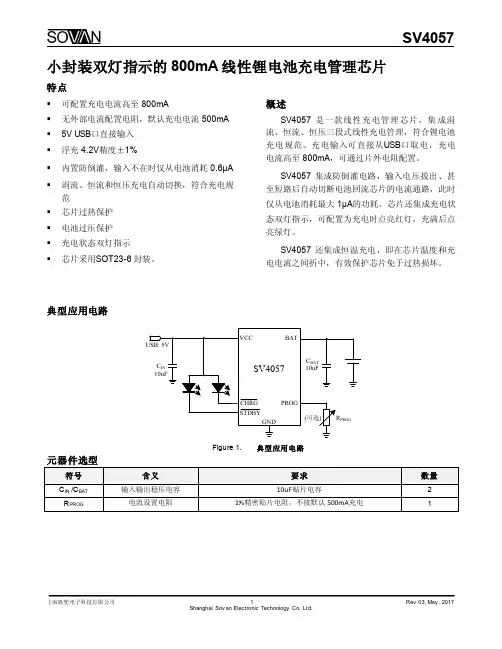
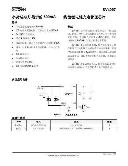
特性◆可编程充电电流500mA◆无需外接MOSFET,检测电阻以及隔离二极管◆用于单节锂电池、采用SOT23-6封装的完整线性充电器◆恒定电流/恒定电压操作,并具有可在无过热危险的情况下实现充电速率最大化的热调节功能。
◆精度达到±1%的4.2V预充电电压◆用于电池电量检测的充电电流监控器输出◆自动再充电◆充电状态双输出、无电池和故障状态显示◆C/10充电终止◆待机模式下的静态电流为25uA◆2.9V涓流充电◆软启动限制浪涌电流应用范围◆移动电话、PDA◆MP3、MP4播放器◆充电器◆数码相机◆电子词典◆蓝牙、GPS导航仪◆便携式设备HE4057采用SOT23-6封装HE4057 500mA线性锂离子电池充电器典型应用打标说明及管脚分布SOT23-6管脚图丝印字符丝印字符说明 左示意图57BM芯片..Y 年号 W 周号 XXXX生产批号管脚描述57BM YWXXXX最大额定值(注)ESD与Latch-up等级结构框图(如果没有特殊说明,环境温度= 25︒C,输入电压=5V)注释(1): 这时处于充电状态,I CC= I VCC- I BAT(2): 这里C/10终止电流门限指的是终止电流与恒流充电电流的比值使用说明HE4057是一款专门为锂离子电池设计的线性充电器,利用芯片内部的功率MOSFET对电池进行恒流/恒压充电。
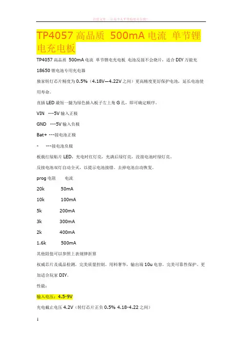
TP4057高品质500mA电流单节锂电充电板TP4057高品质500mA电流单节锂电充电板电池反接不会烧片,适合DIY万能充18650锂电池专用充电器独家转灯芯片精度为0.5%(4.18V—4.22V之间)更高精度更好保护电池,延长电池使用寿命。
直插LED最短一腿为绿色插入板子左上角G孔,即可确定顺序。
VIN ---5V输入正极GND ---5V输入负极Bat+ ---接电池正极- ---接电池负极板载红绿贴片LED,充电时红灯亮,充满后绿灯亮,没接电池时绿灯亮。
反接电池双灯自动全灭,以提示电池接错。
去掉电池自动恢复。
prog电阻电流20k 50mA10k 100mA5k 200mA3k 300mA2k 400mA1.6k 500mA其他阻值可以参照上表规律折算权威芯片及成品检测,完美质量控制。
用料奢华,输出端10u电容。
完美可靠性保护。
更加适合玩家DIY。
性能:输入电压:4.5-9V充电截止电压4.2V(转灯芯片正负0.5% 4.18-4.22之间)输出最大充电电流单颗500mA(可定制更改100-500mA之间)三段式充电,电池在低于2.9V时,涓流预充电,充电电流50mA左右。
电池在2.9V--4.05V恒流充电电池高于4.05V恒压充电,充电电流不断减小。
充电必备知识:1,测试电流的电流表只能串接在充电板的5V输入端。
2,充电电流最好是电池容量的0.37C,就是容量的0.37倍,比如1000mAH的电池充电电流400这样就够了。
过大充电速度快效果就差,冲完了电池电压掉的就多!3,充电连接导线不能过细过长。
这样连接电阻大。
太细的话冲完了电池电压掉的就多。
4,与电池连接最好接触良好。
不然冲完了电池电压掉的就多。
5,如果5V的输入电压偏高,比如5.2甚至5.5,会造成充电电流不足500mA,这是正常的。
小封装的芯片散热性不如大封装。
电压高了芯片发热会自动减小充电电流,不至芯片烧毁。
测试须知:1、空载测试,由于输出端接了100k的上拉电阻,所以在无电池状态下,输出电压在4.5以上,根据电源电压变化。
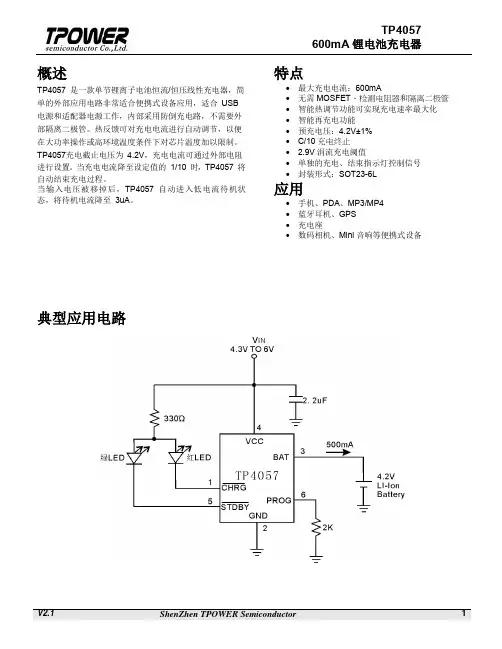
概述TP4057 是一款单节锂离子电池恒流/恒压线性充电器,简单的外部应用电路非常适合便携式设备应用,适合 USB 电源和适配器电源工作,内部采用防倒充电路,不需要外部隔离二极管。
热反馈可对充电电流进行自动调节,以便在大功率操作或高环境温度条件下对芯片温度加以限制。
TP4057充电截止电压为 4.2V ,充电电流可通过外部电阻进行设置。
当充电电流降至设定值的 1/10 时,TP4057 将自动结束充电过程。
当输入电压被移掉后,TP4057 自动进入低电流待机状态,将待机电流降至 3uA 。
特点∙ 最大充电电流:600mA∙ 无需MOSFET 、检测电阻器和隔离二极管 ∙ 智能热调节功能可实现充电速率最大化 ∙ 智能再充电功能 ∙ 预充电压:4.2V±1% ∙ C/10充电终止 ∙ 2.9V 涓流充电阈值∙ 单独的充电、结束指示灯控制信号 ∙封装形式:SOT23-6L应用∙ 手机、PDA 、MP3/MP4 ∙ 蓝牙耳机、GPS ∙充电座∙数码相机、Mini 音响等便携式设备典型应用电路管脚SOT23-6L 定购信息极限参数(注1)注1电气参数(注2,3)注3:规格书的最小、最大规范范围由测试保证,典型值由设计、测试或统计分析保证。
内部框图工作原理TP4057是专门为一节锂离子电池或锂聚合物电池而设计的线性充电器,芯片集成功率晶体管,充电电流可以用外部电阻设定,最大持续充电电流可达1A,不需要另加阻流二极管和电流检测电阻。
TP4057包含两个漏极开路输出的状态指示端,充电状态指示输出端CHRG和充电完成指示输出端STDBY 。
充电时管脚CHRG输出低电平,表示充电正在进行。
如果电池电压低于2.9V,TP4057用小电流对电池进行预充电。
当电池电压超过2.9V时,采用恒流模式对电池充电,充电电流由PROG管脚和GND之间的电阻R PROG确定。
当电池电压接近4.2V电压时,充电电流逐渐减小,TP4057进入恒压充电模式。
TP4057最简单的锂电池充电方案以下是使用TP4057进行锂电池充电的最简单方案:1.原理图首先,我们需要根据TP4057的使用手册来绘制锂电池充电电路的原理图。
原理图包括TP4057芯片、锂电池、外部电阻和一个充电指示灯。
你可以使用一种电路设计软件来完成原理图的设计。
2.PCB布局将原理图转化为PCB布局是非常重要的一步。
你需要将芯片、电阻和其他元件正确地放置在电路板上,并将它们之间的连线连接起来。
在布局的过程中,你需要保证信号和电源线之间的隔离,并按照电流和电源线的规范进行布线。
3.制作电路板一旦PCB布局完成,你可以使用PCB制作工具将电路布线转化为实体电路板。
这可以通过去PCB厂商下订单或者自己使用切割机器和化学法来完成。
4.焊接元件当你获得了电路板后,你需要使用焊接技术将芯片、电阻和其他元件连接到电路板上。
确保焊接质量良好,以保证电路的稳定性。
5.连接电池将锂电池连接到电路板上的电池接口上。
确保极性正确,防止反接。
6.连接充电指示灯将充电指示灯连接到电路板上,并确保其工作正常。
7.测试和调试在将锂电池放入电路板上后,可以通过连接电源来测试电路的工作情况。
确保TP4057正常工作,电池正在充电,并且充电指示灯能够正确显示充电状态。
8.调整充电电流如果你想改变充电电流,你可以更改外部电阻的值。
根据TP4057的手册,选择合适的电阻值并进行更换。
以上就是使用TP4057进行锂电池充电的最简单方案。
当然,根据实际需求,你还可以添加更多的功能和保护措施来提高充电的安全性和效率。
但无论使用何种方案,确保充电过程中关注安全,并遵循相关的规范和标准。

南京拓微集成电路有限公司TP4057特点·锂电池正负极反接保护;·高达500mA的可编程充电电流;·无需MOSFET、检测电阻器或隔离二极管;·用于单节锂离子电池·恒定电流/恒定电压操作,并具有可在无过热危险的情况下实现充电速率最大化的热调节功能;·可直接从USB端口给单节锂离子电池充电;·精度达到±1%的4.2V预设充电电压;·最高输入可达9V;·自动再充电;·2个充电状态开漏输出引脚;·C/10充电终止;·待机模式下的供电电流为40uA;·2.9V涓流充电器件版本;·软启动限制了浪涌电流;·采用6引脚SOT-23封装。
应用·充电座·蜂窝电话、PDA、MP3播放器·蓝牙应用典型应用500mA单节锂离子电池充电器绝对最大额定值·输入电源电压(V CC):-0.3V~9V ·PROG:-0.3V~V CC+0.3V·BA T:-4.2V~7V·CHRG:-0.3V~10V·BA T短路持续时间:连续·BA T引脚电流:500mA·PROG引脚电流:800uA·最大结温:145℃·工作环境温度范围:-40℃~85℃·贮存温度范围:-65℃~125℃·引脚温度(焊接时间10秒):260℃400mA电流完整的充电循环(600mAh)描述TP4057一款完整的单节锂离子电池充电器,带电池正负极反接保护,采用恒定电流/恒定电压线性控制。
其SOT封装与较少的外部元件数目使得TP4057便携式应用的理想选择。
TP4057可以适合USB电源和适配器电源工作。
由于采用了内部PMOSFET架构,加上防倒充电路,所以不需要外部检测电阻器和隔离二极管。
ME4057 1A 锂电池充电管理芯片系列概述ME4057 是一款完整的单节锂离子电池恒压恒流充电管理芯片。
采用带有散热PAD的ESOP8封装形式,外加很少的外部原件,使其成为便携应用的理想选择。
通常可应用在USB电源或适配器电源中。
ME4057不需要电流检测电阻,也不需要外部隔离二极管实现防倒灌应用。
其内部有热反馈电路可以对在充电过程中对芯片温度加以控制。
充电截止电压固定在4.2V/4.34V/4.4V, 充电电流可以外接电阻调节,当充电电流达到恒流电流的1/10时,ME4057将终止充电。
当输入电压(适配器或USB)被拿掉后,ME4057进入睡眠模式。
芯片内部自动关断充电通路,输入电压变低。
此时电池漏电流降低到2uA以下。
当ME4057有电源而电池拿掉时,芯片电流为降低至55uA,来降低系统损耗。
ME4057还具有电池温度检测,输入欠压锁定,自动再充电和两个充电指示引脚。
特点●防电池反接保护功能● 可编程充电电流可达1A●无需MOSFET,检测电阻或隔离二极管●采用ESOP8封装的单节完整线性充电器●恒流恒压切换,内部热反馈保护功能●精度可达±1%的4.2V/4.34V/4.4V 固定充电截止电压●自动再充电功能●充电状态双输出,无电池和故障状态显示● C/10 终止充电● 待机电流55μA● 2.9V涓流切换阈值● 软启动限制浪涌电流● 电池温度监测功能应用场合●移动电话●数码相机● MP3,MP4播放器●蓝牙应用●便携设备● USB电源,适配器封装形式● 8-pin ESOP8典型充电周期图 (1000mAh 电池)0.250.50.75 1.0 1.25 1.5 1.75 2.020040060080010001200 2.753.003.253.503.754.004.254.50时间(小时)充电电流(m A )充电电压(V )选购指南ME 40 57 X XX G浮充电压A/B :4.2V D :4.34V E :4.4V环保标识产品品种号产品类别号公司标志封装形式SP :ESOP8芯片脚位图TEMP PROG GND VCCCECHRGSTDBYBAT ESOP8脚位说明芯片功能示意图绝对最大额定值注意:绝对最大额定值是本产品能够承受的最大物理伤害极限值,请在任何情况下勿超出该额定值。
南京拓微集成电路有限公司TP4057特点·锂电池正负极反接保护;·高达500mA的可编程充电电流;·无需MOSFET、检测电阻器或隔离二极管;·用于单节锂离子电池·恒定电流/恒定电压操作,并具有可在无过热危险的情况下实现充电速率最大化的热调节功能;·可直接从USB端口给单节锂离子电池充电;·精度达到±1%的4.2V预设充电电压;·最高输入可达9V;·自动再充电;·2个充电状态开漏输出引脚;·C/10充电终止;·待机模式下的供电电流为40uA;·2.9V涓流充电器件版本;·软启动限制了浪涌电流;·采用6引脚SOT-23封装。
应用·充电座·蜂窝电话、PDA、MP3播放器·蓝牙应用典型应用500mA单节锂离子电池充电器绝对最大额定值·输入电源电压(V CC):-0.3V~9V ·PROG:-0.3V~V CC+0.3V·BA T:-4.2V~7V·CHRG:-0.3V~10V·BA T短路持续时间:连续·BA T引脚电流:500mA·PROG引脚电流:800uA·最大结温:145℃·工作环境温度范围:-40℃~85℃·贮存温度范围:-65℃~125℃·引脚温度(焊接时间10秒):260℃400mA电流完整的充电循环(600mAh)描述TP4057一款完整的单节锂离子电池充电器,带电池正负极反接保护,采用恒定电流/恒定电压线性控制。
其SOT封装与较少的外部元件数目使得TP4057便携式应用的理想选择。
TP4057可以适合USB电源和适配器电源工作。
由于采用了内部PMOSFET架构,加上防倒充电路,所以不需要外部检测电阻器和隔离二极管。
锂电池在使用中随着电量的释放,电压下降,电池的化学活性也会降低。
为了更好的保护锂电池的性能,锂电池一般会要求充电过程按涓流充电(低压预充)、恒流充电、恒压充电以及充电终止四个阶段,进行管控。
一般锂电池标称电压是3.7V,放电终止电压的2.75V,充电终止电压是4.20V。
给锂电池充电时需要的基本要求就是各个阶段特定的充电电压和充电电流,有的增加些其他的辅助功能都是为了改善电池的寿命。
市面上有很多专业的管理锂电池充电的芯片,他们大多都是采用限压恒流的方式控制电源给电池充电。
典型的充电过程是:.检测待充电电池的电压,如果电压低于3V预充电电压,先要进行预充电,充电电流要求不大于0.1C,一般为0.05C左右,待电压升到3V后,进入标准充电过程,标准充电过程如下:.以设定的电流进行恒流充电,一般电流设置为0.2C~1C(比如一个1000mAh的电池就设置在100mA~1000mA)之间,充到电池电压升到4.20V时,.改为恒压充电,保持充电电压为4.20V.此时,充电电流逐渐下降至预充电电流时,充电结束。
锂电池充电曲线如下图:图中蓝线表示充电电流,红色虚线表示锂电池电压,从图中可以看出四个充电过程。
通过上面的了解,锂电池正确的充电过程是一个有点复杂的过程,我们实际中都是采用市场上专业的锂电池充电管理芯片来对锂电池进行充电。
单节线性锂电池充电芯片TP4057下面就介绍一款常用锂电池充电芯片TP4057,实际应用中可以根据自己需求选择其他型号的充电IC,原理都是大同小异。
我们先看一下TP4057对锂电池的充电曲线图吧。
可以看出这个充电曲线和前面介绍的几乎完全一样。
我们再来看下TP4057内部框图TP4057引脚图及引脚描述如下:典型应用电路图如下:恒流充电阶段时的充电电流计算:Rprog=1000/IBAT(IBAT<=0.3A)实际应用中根据需求选择合适的Rprog。
Rprog与充电电流的关系确定可参考下表:我们可以根据这个TP4057典型应用电路自己搭建一个锂电池充电电路,这样锂电池的充电安全放心,寿命也不会减少太快。
基于TP4057的USB锂电池充电电路及PCB原理图TP4057简介:TP4057是单节锂电池充电管理芯片,输入电压为4V ~ 9V,典型值为5V,可改变TP4057的6脚电阻来控制充电电流,计算公式为RPROG =1000/IBAT(当IBAT <300毫安时)、RPROG =1300/IBAT -1000(当IBAT>300毫安时),调节范围100 ~ 500毫安,截止充电电压4.2V,外围简单,无须外接开关管,具有充电指示和充满指示、防电池反接、电源欠压保护等功能。
TP4057充电过程:TP4057的充电过程大致如下:当待充电电池接入后,若电池电压小于2.9V,则TP4057将对电池进行预充电,电流为设定电流的1/10,当电池电压上升到2.9V 后,TP4057开始按设定电流恒流充电,当电压上升到4.1V(大概冲到了80%~90%)后恒流充电过程结束,输出电压恒定在4.2V,输出电流降低到设定电流的1/10,开始恒压充电过程,当电池电压达到4.2V后,充电过程完成,此后TP4057将连续监测电池电压,若电池电压下降到4.1V,则会再次进入充电过程,对电池进行充电。
模块简介:该充电模块输入使用miniUSB供电,板上恒流充电电流设定电阻标记为1.6K,对应充电电流为500毫安,指示灯可以选用3mm直插LED,或1005封装的贴片LED,TP4057应紧贴PCB,以便良好散热,当TP4057内部温度超过设定值(约120℃)后,芯片将自动减小充电电流,防止芯片过热烧毁。
模块指示灯信息:状态红灯CHRG 绿灯STDBY充电状态亮灭充电完成灭亮电源欠压电池反接灭灭无电池闪烁亮该模块可用制作简单的锂电池充电器。
模块尺寸:25.5mm*12mm 单面板。
具有热调节功能单片双灯显示的微型线性电池管理芯片■产品概述XT4057是一个完善的单片锂离子电池恒流/恒压线形电源管理芯片。
它薄的尺寸和小的外包装使它便于便携应用。
更值得一提的是,XT4057专门设计适用于USB的供电规格。
得益于内部的MOSFET结构,在应用上不需要外部电阻和阻塞二极管。
在高能量运行和高外围温度时,热反馈可以控制充电电流以降低芯片温度。
充电电压被限定在4.2V,充电电流通过外部电阻调节。
在达到目标充电电压后,当充电电流降低到设定值的1/10时,XT4057就会自动结束充电过程。
当输入端(插头或USB 提供电源)拔掉后,XT4057自动进入低电流状态,电池漏电流将降到2µA以下。
XT4057还可被设置于停止工作状态,使电源供电电流降到25µA。
XT4057采用独特的内部专利结构确保了电池接反时芯片自动进入保护状态,确保IC不被击穿导致电池自放电引起事故。
其余特性包括:充电电流监测,输入低电压闭锁,自动重新充电和充电已满及开始充电的标志。
■用途●手机,PDA,MP3●蓝牙应用■产品特点●可编程使充电电流可达500mA.●不需要MOSFET,传感电阻和阻塞二极管●小的尺寸实现对锂离子电池的完全线形充电管理●恒电流/恒电压运行和热度调节使得电池管理效力最高,没有热度过高的危险●从USB接口管理单片锂离子电池●预设充电电压为4.2V 1%●充电电流输出监控●充电状态指示标志●1/10充电电流终止●停止工作时提供25µA电流● 2.9V涓流充电阈值电压●软启动限制浪涌电流●电池反接保护■封装●SOT23-6L■典型应用电路VINGND GND 注:C1=4.7uF,C2=10uF,IBAT = (V PROG/R PROG)*1000■ 订购信息■ 引脚配置CHRG GND BAT PROGSOT23-6L (TOP VIEW)VIN123465DONE■ 引脚分配■ 引脚功能PROG (引脚6):充电电流编程,充电电流监控和关闭端。
TP5000 TP4060 TP4056 充丰○R充电模块说明书(1v8)淘宝店:https:///TP5000 TP4060 TP4056 充电模块说明书本公司生产的充电模块, 均选用南京拓微集成电路有限公司原厂芯片, 核心电路设计按原厂设计,TP5000小板额外增加了电池接反保护电路。
小板均为黄色, 有1 USB公头和1个安装孔. 可以直接焊上一个USB公头(USB头安装在器件背面,如封面照片), 安装孔可以用来固定到散热器上。
充满亮蓝色LED指示灯, 充电中亮红色灯。
其他状态请参照芯片厂家说明文档。
淘宝购买链接: https:///item.htm?id=5219200897923种充电板参数对照表:TP4056 0.9A 5V 线性 很热 无,接反烧 不可 30mm X 16mmTP4060 0.75A 5V 线性 很热 有 不可 30mm X 16mmTP5000 2A 5V-9V 开关 会热 已加防接反 可以设置35mm X 16mm接反保护指充电输出端, 输入端正负极接反均会烧毁.设计风格如下:TP5000 充电模块使用开关电源技术, 充电效率高, 主芯片充电时会发少量发热, 源芯片没有电池接反保护, 模块输出加了接反保护电路。
能给4.2V的锂离子电池充电(默认设置), 也能给铁锂电池3.6V充电(R1电阻去掉), 不能直接用来测电池充电的安时数(AH)数, 但可以用来测瓦时(WH)数; 注意:加接USB头后,插入的电源(充电器,充电头) 应该要有2A或以上的供电能力。
使用了一体式密封电感, 钽电容。
最大特点是充电速度快! 适合充大容量电池\优质电池。
模块尺寸: 35mm X 16mm充电会发热, 很热, 输出接反会有保护。
只能给4.2V的锂离子电池充电, 可以配合其他表用来测电池充电的安时数(AH)数,也可以用来测瓦时(WH), 加接USB头后;注意:加接USB头后,插入的电源(充电器,充电头) 应该要有1A或以上的供电能力。
March 2012Doc ID 022842 Rev 11/13AN4057Application noteSPC560Pxx, SPC56APxx power up HW guidelineINTRODUCTIONThis application note is addressed to system hardware designers usingSTMicroelectronics ® SPC560Pxx/SPC56APxx microcontrollers It gives design references to ensure a reliable microcontroller power up sequence also in the condition of an offset voltage on the high voltage regulator supply pin V DD_HV_REG at power up.The use of the SPC560Pxx/SPC56APxx internal voltage regulator requires a specific design ST approved ballasts with the recommended supporting network described in the latest revision of the device data sheet (for further details see Section Appendix A: Additional information ). It is important to respect the power on sequence conditions, ensuring a monotonic supply ramp starting at ground level and respecting the min and max slew rate on V DD_HV_REG .This application note covers:■Recommended power on sequence conditions ■Possible deviations injecting an offset voltage on V DD_HV_REG and its impact on microcontroller power up ■Optional proposals to eliminate the effect of offset voltage on V DD_HV_REG pinContents AN4057Contents1Overview . . . . . . . . . . . . . . . . . . . . . . . . . . . . . . . . . . . . . . . . . . . . . . . . . . 51.1Power up sequencing . . . . . . . . . . . . . . . . . . . . . . . . . . . . . . . . . . . . . . . . . 52Offset voltage on V DD_HV_REG and voltage regulator circuitry . . . . . . . 62.1Offset voltage on V DD_HV_REG: problem description . . . . . . . . . . . . . . . . . 62.1.1Possible application paths to induce a V DD_HV_REG offset voltage . . . . . 62.1.2Battery short to pin on connector of microcontroller board . . . . . . . . . . . 62.2HW guidelines for high/low voltage supply of the internal regulator with offsetvoltage on V DD_HV_REG 72.2.1Resistors partition network . . . . . . . . . . . . . . . . . . . . . . . . . . . . . . . . . . . 72.2.2V DD_HV_REG pin active path to ground . . . . . . . . . . . . . . . . . . . . . . . . . . . 8 3SPC560Pxx/SPC56APxx devices affected . . . . . . . . . . . . . . . . . . . . . . 10Appendix A Additional information. . . . . . . . . . . . . . . . . . . . . . . . . . . . . . . . . . . . 11A.1Reference document. . . . . . . . . . . . . . . . . . . . . . . . . . . . . . . . . . . . . . . . . 11 Revision history . . . . . . . . . . . . . . . . . . . . . . . . . . . . . . . . . . . . . . . . . . . . . . . . . . . . 122/13Doc ID 022842 Rev 1AN4057List of tables List of tablesTable 1.Resistor partition network values . . . . . . . . . . . . . . . . . . . . . . . . . . . . . . . . . . . . . . . . . . . . . 8 Table 2.SPC560Pxx/SPC56APxx device affected from V DD_HV_REG offset issue . . . . . . . . . . . . . 10 Table 3.Document revision history . . . . . . . . . . . . . . . . . . . . . . . . . . . . . . . . . . . . . . . . . . . . . . . . . 12Doc ID 022842 Rev 13/13List of figures AN4057 List of figuresFigure 1.Offset voltage on V DD_HV_REG from SPC560Pxx/SPC56APxx input pin . . . . . . . . . . . . . . . 6 Figure 2.Battery short to pin on connector of microcontroller board. . . . . . . . . . . . . . . . . . . . . . . . . . 7 Figure 3.Resistors partition network. . . . . . . . . . . . . . . . . . . . . . . . . . . . . . . . . . . . . . . . . . . . . . . . . . 8 Figure 4.Active path to ground . . . . . . . . . . . . . . . . . . . . . . . . . . . . . . . . . . . . . . . . . . . . . . . . . . . . . . 9 4/13Doc ID 022842 Rev 1AN4057Overview Doc ID 022842 Rev 15/131 OverviewThese SPC560Pxx /SPC56APxx microcontrollers are members of a new microcontrollerfamily built on the Power Architecture ®. The device is supplied externally with a singlevoltage supply, which can be either 5V or 3.3V depending on application requirements.Internally the chip operates with 2 supply voltages, namely the main supply (5V or 3.3V)and the core logic supply (1.2V).This document provides guideline for the recommended configuration of the high and lowvoltage supply for the internal regulator in order to ensure the correct power up sequence ofthe microcontroller.The note describes application fault conditions that may offset V DD_HV_REG significantly andmitigating circuitries to ensure reliable power up in case of these fault conditions. Thestandard supply circuitry and sequence that use in the recommended conditions of initialpower up on V DD_HV_REG pin starting from ground level are described in theSPC560Pxx/SPC56APxx data sheet (for further details see Section Appendix A: Additionalinformation ).Possible causes of fault conditions injecting an offset voltage on V DD_HV_REG pin aredescribed in the following list:●Supply microcontrollers I/O V IN while the microcontroller is switched off with shorted supply for V DD_HV_REG and V DD_HV_IO pins ●Offset voltage injected on V DD_HV_REG by external signal(s) shorted to battery.1.1 Power up sequencingPreventing an overstress event or a malfunction within and outside the device, theSPC560Pxx/SPC56APxx implements a specific power up sequence, as described in thedata sheet, to ensure each module is started only when all conditions for switching it ON areavailable.In case of a fault condition on the application board, that sequence may not be respected,causing the device not to exit the power up.Two possible fault conditions are described in the following sections. However, if the faultcause is removed, the device (while within the absolute maximum ratings) works again,without getting damaged, powering up properly.2 Offset voltage on V DD_HV_REG and voltage regulatorcircuitry2.1 Offset voltage on V DD_HV_REG: problem descriptionV DD_HV_REG offset on the devices SPC560Pxx/SPC56APxx, before the module is poweredup, may in some cases prevent the power up device correctly.A V DD_HV_REG offset before a correct power up supply sequence can set the POR devicelogic to an undefined state, preventing the internal logic to switch correctly and initialize theinternal V DD_LV circuitry. The internal regulator remains in power down. The consequence isthat the microcontroller is not able to exit reset.application paths to induce a V DD_HV_REG offset voltage2.1.1 PossibleFigure1 describes a GPIO configuration with the pin connected to an externally suppliedsignal (V batt).If V batt is powered while MCU V DD is not yet provided, GPIO protection circuitry (diode)induces a voltage on V DD_HV_IO.In the case V DD_HV_IO is directly connected to V DD_HV_REG, the induced voltage ispropagated to the internal regulator. The same consideration is done when using anexternal diode, D1 in Figure1, connecting GPIO V IN to V DD.2.1.2 Battery short to pin on connector of microcontroller boardAnother possible cause of an initial offset on V DD_HV_REG is battery short to any pin of theboard connector.6/13Doc ID 022842 Rev 1The short to battery can be propagated through various components (ASSP, ASICs, ComDrivers) to the V DD_HV_REG as these components typically share the same supply.2.2 HW guidelines for high/low voltage supply of the internalregulator with offset voltage on V DD_HV_REGIn general an offset voltage must be avoided to pre-charge V DD_HV_REG through parasiticpaths. The MCU supply must power on from GND to power supply with a monotonic ramprate, minimum and maximum value as described in the data sheet (T vdd). In case of a faultcondition, injecting an offset to V DD_HV_REG while the MCU is not supplied, the followingmodifications on the module can prevent the device to remain in reset. The supply voltageconditions are still respected.Possible HW solutions on the supplying circuitry of the microcontroller to allow a correctpower up sequence, in case of an offset build up on V DD_HV_REG pin are:●Resistive network between V DD_HV_REG, V DD_LV_REG and GND●Active discharge on V DD or V DD_HV_REG at power up●Other application means to prevent the presence of an offset on V DD_HV_REG duringpower upnetwork2.2.1 ResistorspartitionThis solution with two partitioning resistors, shown in Figure3, enables V DD_LV_REG to bepre- conditioned and the internal V DD_LV_REG to be forced into a defined state as soon asthe ballast regulator turns-on.Doc ID 022842 Rev 17/138/13Doc ID 022842 Rev 1Static consumption has to be considered into the board voltage regulator design.2.2.2 V DD_HV_REG pin active path to groundAnother solution is to add a controlled active path to ground on V DD_HV_REG /V DD_HV_IO thatforces these pins to ground when the microcontroller is switched off or discharges theV DD_HV_REG at start up.Figure 4 describes a generic configuration that uses the enable signal of an externalregulator, VIGN, to drive the gate of NFET to force V DD_HV_REG /V DD_HV_IO pin to ground.When the external regulator is off there is a discharge path of the current from theV DD_HV_REG /V DD_HV_IO .It has to be granted that the V DD rises with the required monotonic slew rate before any faultcondition can build up an offset on V DD_HV_REG , prior to the release of the active dischargecircuit.Table 1.Resistor partition network valuesSymbolParameter Value Unit V DD_HV_REG @ 5V R1Resistor between V DD_HV_REG /ballastemitter and ballast collector910ΩR2Resistor between ballast emitter andground300ΩV DD_HV_REG @ 3.3V R1Resistor between V DD_HV_REG /ballastemitter and ballast collector510ΩR2Resistor between ballast emitter andground 300ΩDoc ID 022842 Rev 19/13SPC560Pxx/SPC56APxx devices affected AN405710/13Doc ID 022842 Rev 13 SPC560Pxx/SPC56APxx devices affectedTable 2 lists the STMicroelectronics SPC560Pxx/SPC56APxx devices and revisions that areaffected by the previously described phenomenon.Table 2.SPC560Pxx/SPC56APxx device affected from V DD_HV_REG offset issuePart number Package devicemarking mask identifierand silicon versionMIDR1 register SPC560P34xx/P40xx AB -cut 1.1 (and older)MAJOR_MASK[3:0]: 4'b0000MINOR_MASK[3:0]: 4'b0001SPC560P50xx/P44xx BD -cut 3.4 (and older)MAJOR_MASK[3:0]: 4’b0001MINOR_MASK[3:0]: 4’b0101SPC560P60xx/P54xx SPC56AP60xx/AP54xxAA -cut 1.0 MAJOR_MASK[3:0]: 4’b0000MINOR_MASK[3:0]: 4’b0000AN4057Additional information Doc ID 022842 Rev 111/13Appendix A Additional informationA.1 Reference document●32-bit Power Architecture ® based MCU with 1088 KB Flash memory and 80 KB RAMfor automotive chassis and safety applications (SPC560P54x, SPC560P60L3,SPC56AP54L3, SPC56AP60x, Doc ID 18340)●32-bit Power Architecture ® based MCU with 320 KB Flash memory and 20 KB RAM forautomotive chassis and safety applications (SPC560P34L1, SPC560P34L3,SPC560P40L1, SPC560P40L3, Doc ID 16100)●32-bit Power Architecture ® based MCU with 576 KB Flash memory and 40 KB SRAMfor automotive chassis and safety applications (SPC560P44L3, SPC560P44L5,SPC560P50L3, SPC560P50L5, Doc ID 14723)Revision history AN4057 Revision historyTable 3.Document revision historyDate Revision Changes01-Mar-20121Initial release.12/13Doc ID 022842 Rev 1AN4057Please Read Carefully:Information in this document is provided solely in connection with ST products. STMicroelectronics NV and its subsidiaries (“ST”) reserve the right to make changes, corrections, modifications or improvements, to this document, and the products and services described herein at any time, without notice.All ST products are sold pursuant to ST’s terms and conditions of sale.Purchasers are solely responsible for the choice, selection and use of the ST products and services described herein, and ST assumes no liability whatsoever relating to the choice, selection or use of the ST products and services described herein.No license, express or implied, by estoppel or otherwise, to any intellectual property rights is granted under this document. If any part of this document refers to any third party products or services it shall not be deemed a license grant by ST for the use of such third party products or services, or any intellectual property contained therein or considered as a warranty covering the use in any manner whatsoever of such third party products or services or any intellectual property contained therein.UNLESS OTHERWISE SET FORTH IN ST’S TERMS AND CONDITIONS OF SALE ST DISCLAIMS ANY EXPRESS OR IMPLIED WARRANTY WITH RESPECT TO THE USE AND/OR SALE OF ST PRODUCTS INCLUDING WITHOUT LIMITATION IMPLIED WARRANTIES OF MERCHANTABILITY, FITNESS FOR A PARTICULAR PURPOSE (AND THEIR EQUIVALENTS UNDER THE LAWS OF ANY JURISDICTION), OR INFRINGEMENT OF ANY PATENT, COPYRIGHT OR OTHER INTELLECTUAL PROPERTY RIGHT. UNLESS EXPRESSLY APPROVED IN WRITING BY TWO AUTHORIZED ST REPRESENTATIVES, ST PRODUCTS ARE NOT RECOMMENDED, AUTHORIZED OR WARRANTED FOR USE IN MILITARY, AIR CRAFT, SPACE, LIFE SAVING, OR LIFE SUSTAINING APPLICATIONS, NOR IN PRODUCTS OR SYSTEMS WHERE FAILURE OR MALFUNCTION MAY RESULT IN PERSONAL INJURY, DEATH, OR SEVERE PROPERTY OR ENVIRONMENTAL DAMAGE. ST PRODUCTS WHICH ARE NOT SPECIFIED AS "AUTOMOTIVE GRADE" MAY ONLY BE USED IN AUTOMOTIVE APPLICATIONS AT USER’S OWN RISK.Resale of ST products with provisions different from the statements and/or technical features set forth in this document shall immediately void any warranty granted by ST for the ST product or service described herein and shall not create or extend in any manner whatsoever, any liability of ST.ST and the ST logo are trademarks or registered trademarks of ST in various countries.Information in this document supersedes and replaces all information previously supplied.The ST logo is a registered trademark of STMicroelectronics. All other names are the property of their respective owners.© 2012 STMicroelectronics - All rights reservedSTMicroelectronics group of companiesAustralia - Belgium - Brazil - Canada - China - Czech Republic - Finland - France - Germany - Hong Kong - India - Israel - Italy - Japan - Malaysia - Malta - Morocco - Philippines - Singapore - Spain - Sweden - Switzerland - United Kingdom - United States of AmericaDoc ID 022842 Rev 113/13。
特点·高达1000mA的可编程充电电流·无需MOSFET、检测电阻器或隔离二极管·用于单节锂离子电池、采用SOP封装的完整线性充电器·恒定电流/恒定电压操作,并具有可在无过热危险的情况下实现充电速率最大化的热调节功能·精度达到±1%的4.2V预设充电电压·用于电池电量检测的充电电流监控器输出·自动再充电·充电状态双输出、无电池和故障状态显示·C/10充电终止·待机模式下的供电电流为55uA·2.9V涓流充电·软启动限制了浪涌电流·电池温度监测功能·采用8引脚SOP-PP封装TEMP(引脚1):电池温度检测输入端。
将TEMP管脚接到电池的NTC传感器的输出端。
如果TEMP管脚的电压小于输入电压45%或者大于输入电压的80%,意味着电池温度过低或过高,则充电被暂停。
如果TEMP 直接接GND,电池温度检测功能取消,其他充电功能正常。
PROG(引脚2):恒流充电电流设置和充电电流监测端。
从PROG管脚连接一个外部电阻到地端可以对充电电流进行编程。
在预充电阶段,此管脚的电压被调制在0.1V;在恒流充电阶段,此管脚的电压被固定在1V。
客户应用中,可根据需求选取合适大小的RPROGRPROG与充电电流的关系确定可参考下表:GND(引脚3):电源地。
Vcc (引脚4):输入电压正输入端。
此管脚的电压为内部电路的工作电源。
当Vcc与BAT管脚的电压差小于30mV时,TP4056将进入低功耗的停机模式,此时BAT 管脚的电流小于2uABAT(引脚5):电池连接端。
将电池的正端连接到此管脚。
在芯片被禁止工作或者睡眠模式,BAT管脚的漏电流小于2uA。
BAT管脚向电池提供充电电流和4.2V 的限制电压.STDBY(引6):电池充电完成指示端。
当电池充电完成时STDBY被内部开关拉到低电平,表示充电完成。