NA555DR中文资料
- 格式:pdf
- 大小:360.91 KB
- 文档页数:24


NE555中文资料通用时基电路NE555P概述:封装外形图NE555P是一块通用时基电路,电路包含24个晶体管,2 个二极管和17个电阻,组成阈值比较器,触发比较器,RS 触发器,复位输入,放电和输出等6部分。
采用DIP8、S0P8封装形式。
主要特点:关闭时间小于2 S o最大工作频率大于500kHz。
定时可从微秒级至小时级(由外接电阻电容精确控制)可工作于振荡方式或单稳态方式。
输出电流大,200mA (可提供或灌入)。
占空比可调。
可同TTL电路相接。
温度稳定性好,0.005%/C功能框图极限值(绝对最大额定值,若无其它规定,Tamb=25C)(若无其它规定,Vcc=5~15V , Tamb=25应用图555芯片引脚图及引脚描述555的8脚是集成电路工作电压输入端,电压为5〜18V ,以UCC 表示;从分压器上看出,上比较器6脚A1的5脚接在 R1和R2之间,所以5脚的电压固定在 2UCC/3上;下比 较器A2接在R2与R3之间,A2的同相输入端电位被固定在 UCC/3上。
NE555管脚功能介绍:1脚为地。
2脚为触发输入端;3脚为输出端,输出的电平状态受触发器控制,而触发 器受上比较器6脚和下比较器2脚的控制。
当触发器接受上比较器 A1从R 脚输入的高电平时,触发器被置于复位状态, 3脚输出低电平;2脚和6脚是互补的,2脚只对低电平起作用,高电平对它不起作用,即电压小于1UCC/3 , 此时3脚输出高电平。
6脚为阈值端,只对高电平起作用,低电平对它不起作用,即输入 电 压大于2 Ucc/3,称高触发端,3脚输出低电平,但有一个先决条件,即 2脚电位必须大于1.单稳态延时电路V ;TVo -)丄工3.开机延迟电路:接通电源输岀Vo 由低跳变到高而延迟的电路。
延迟时间:td=1.1RCVo丄HFUAU o0. 01 uF 1 01WIH-O Vc c启动4.开机延迟电路:接通电源输岀 由高跳变到低而延迟的电路。


E53NA50中文资料STE53NA50N -CHANNEL ENHANCEMENT MODEFAST POWER MOS TRANSISTORs TYPICAL R DS(on)=0.075?s HIGH CURRENT POWER MODULE s AVALANCHE RUGGED TECHNOLOGYsVERY LARGE SOA -LARGE PEAK POWER CAPABILITYs EASY TO MOUNTsSAME CURRENT CAPABILITY FOR THE TWO SOURCE TERMINALSs EXTREMELY LOW Rth (Junction to case)sVERY LOW INTERNAL PARASITIC INDUCTANCEsISOLATED PACKAGE UL RECOGNIZEDAPPLICATIONS s SMPS &UPS s MOTOR CONTROL s WELDING EQUIPMENT s OUTPUT STAGE FOR PWM,ULTRASONIC CIRCUITSINTERNAL SCHEMATIC DIAGRAMFebruary 1998ABSOLUTE MAXIMUM RATINGSSymbol ParameterValue Unit V DS Drain-source Voltage (V GS =0)500V V DGR Drain-gate Voltage (R GS =20k ?)500V V GS Gate-source Voltage ±30V I D Drain Current (continuous)at T c =25oC 53A ID Drain Current (continuous)at T c =100o C 33A I DM(?)Drain Current (pulsed)212A P to t Total Dissipation at T c =25oC 460W Derating Factor 3.68W/o CT st g Storage Temperature-55to 150o C T j Max.Operating Junction Temperature 150oCV ISOInsulation Withhstand Voltage (AC-RMS)2500V (?)Pulse width limited by safe operating areaTYPE V DSS R DS(on)I D STE53NA50500V<0.085?53AISOTOP1/7THERMAL DATAR t hj-ca se R thc-h Thermal Resistance Junction-case Max Thermal Resistance Case-heatsink With ConductiveGrease Applied Max0.270.05o C/Wo C/WAVALANCHE CHARACTERISTICSSymbol Parameter Max Value UnitI AR Avalanche Current,Repetitive or Not-Repetitive(pulse width limited by T j max,δ <1%)26AE AS Single Pulse Avalanche Energy(starting T j=25o C,I D=I AR,V DD=50V)1014mJELECTRICAL CHARACTERISTICS(T case=25o C unless otherwise specified)OFFSymbol Parameter Test Conditions Min.Typ.Max.Unit V(BR)DSS Drain-sourceBreakdown VoltageI D=1mA V GS=0500VI DSS Zero Gate VoltageDrain Current(V GS=0)V DS=Max RatingV DS=Max Rating T c=125o C1001000μAμAI GSS Gate-body LeakageCurrent(V DS=0)V GS=±30V±400nA ON(?)Symbol Parameter Test Conditions Min.Typ.Max.Unit V GS(th)Gate ThresholdVoltageV DS=V GS I D=1mA 2.253 3.75VR DS(on)Static Drain-source OnResistanceV GS=10V I D=27A0.0750.085?I D(o n)On State Drain Current V DS>I D(on)x R DS(on)maxV GS=10V53A DYNAMICSymbol Parameter Test Conditions Min.Typ.Max.Unit g fs(?)ForwardTransconductanceV DS>I D(on)X RDS(on)MAX I D=27A25SC iss C oss C rss Input CapacitanceOutput CapacitanceReverse TransferCapacitanceV DS=25V f=1MHz V GS=0131500450162000650nFpFpFSTE53NA50 2/7ELECTRICAL CHARACTERISTICS(continued) SWITCHING ONSymbol Parameter Test Conditions Min.Typ.Max.Unit t d(on) t r Turn-on TimeRise TimeV DD=250V I D=27AR G=4.7 ?V GS=10V(see test circuit,figure1)579280130nsnsQ g Q gs Q gd Total Gate ChargeGate-Source ChargeGate-Drain ChargeV DD=400V I D=53A V GS=10V47054219658nCnCnCSWITCHING OFFSymbol Parameter Test Conditions Min.Typ.Max.Unit t r(Vof f) t ft c Off-voltage Rise TimeFall TimeCross-over TimeV DD=400V I D=53AR G=4.7 ?V GS=10V(see test circuit,figure3)1053614514550205nsnsnsSOURCE DRAIN DIODESymbol Parameter Test Conditions Min.Typ.Max.Unit I SD I SDM(?)Source-drain CurrentSource-drain Current(pulsed)53212AAV SD(?)Forward On Voltage I SD=53A V GS=0 1.6V t rr Q rr I RRM Reverse RecoveryTimeReverse RecoveryChargeReverse RecoveryCurrentI SD=53A di/dt=100A/μsV R=100V T j=150o C(see test circuit,figure3)100031.563nsμCA(?)Pulsed:Pulse duration=300μs,duty cycle1.5% (?)Pulse width limited by safe operating areaSafe Operating Area for Thermal ImpedanceSTE53NA503/7Output Characteristics TransconductanceGate Charge vs Gate-source Voltage Transfer Characteristics Static Drain-source On Resistance Capacitance VariationsSTE53NA50 4/7Normalized Gate Threshold Voltage vs TemperatureSource-drain Diode Forward Characteristics Fig.2:Gate Charge test Circuit Normalized On Resistance vs Temperature Fig.1:Switching Times Test Circuits For Resistive Load Fig.3:Test Circuit For Inductive Load Switching And Diode Recovery TimesSTE53NA505/7DIM.mm inch MIN.TYP.MAX.MIN.TYP.MAX.A 11.812.20.4660.480B 8.99.10.3500.358C 1.95 2.050.0760.080D 0.750.850.0290.033E 12.612.80.4960.503F 25.1525.50.990 1.003G 31.531.71.240 1.248H 40.157J 4.1 4.30.1610.169K 14.915.10.5860.594L 30.130.31.185 1.193M 37.838.21.488 1.503N 40.157O7.88.20.3070.322BEHONJ K L MFACGDISOTOP MECHANICAL DATASTE53NA506/7Information furnished is believed to be accurate and reliable.However,SGS-THOMSON Microelectronics assumes no responsability for the consequences of use of such information nor for any infringement of patents or other rights of third parties which may results from its use.No license is granted by implication or otherwise under any patent or patent rights of SGS-THOMSON Microelectronics.Specifications mentioned in this publication are subject to change without notice.This publication supersedes and replaces all information previously supplied.SGS-THOMSON Microelectronics products are not authorized for use as critical components in life support devices or systems without express written approval of SGS-THOMSON Microelectonics.1998SGS-THOMSON Microelectronics -Printed in Italy -All Rights ReservedSGS-THOMSON Microelectronics GROUP OF COMPANIESAustralia -Brazil -Canada -China -France -Germany -Italy -Japan -Korea -Malaysia -Malta -Morocco -The Netherlands -Singapore -Spain -Sweden -Switzerland -Taiwan -Thailand -United Kingdom -U.S.A...STE53NA50 7/7。

一个完整555 定时器基本指南一个完整555 定时器基本指南发布: | 作者:——| 来源: 华强| 查看:11648 次| 用户关注:本IC 是一个单片定时电路,可以产生精确和高度稳定的时间延误或振荡。
像其他常用的运算放大器,该IC 还非常可靠,易于使用,成本便宜。
它有一个应用,包括各种单稳态和非稳态多谐振荡器,DC - DC 转换器,数字逻辑探针,波形发生器,模拟频率计和转速表,温度测量和控制设备,稳压器等。
本文涵盖了所有的555 定时器IC 的基本方面。
您可能已经知道,SE / 东北555 Signetics 公司公司介绍了1970 年的一个定时器IC 。
在这篇文章中,我们涵盖约555 定时器IC 的以下信息。
1 。
介绍555 定时器IC(2)555 定时器IC 引脚配置(3)555 定时器的基础4。
框图5 ,工作原理6,下载数据手册1。
555 定时器IC 其中最通用的线性IC ,这是第一次在1970 年年初推出Signetic 给公司作为名义东南/东北555 定时器555 定时器。
本IC 是一个单片定时电路,可以产生精确和高度稳定的时间延误或振荡。
像其他常用的运算放大器,该IC 还非常可靠,易于使用,成本便宜。
它有一个应用,包括各种单稳态和非稳态多谐振荡器,DC - DC 转换器,数字逻辑探针,波形发生器,模拟频率计和转速表,温度测量和控制设备,稳压器等。
计时器基本上工作在两种模式之一,无论是作为一个单稳态多谐振荡器(一次性),或作为一个非稳态(自由运行)multivibrator.The SE 555 设计的工作温度范围从-55 ° C 125 °而东北555的工作温度范围0 °170 ' C555 定时器的重要特点是:从广泛到18 伏的电源电压范围从+ 5 伏特的电源。
下沉或采购200 毫安的负载电流。
所以只有很少的外部元件的正确选择允许超过几百公斤赫兹的频率几分钟的时间间隔,几分钟的时间间隔可分为,应正确选择外部元件。


555芯片zvs电路555芯片ZVS电路引言:555芯片是一种非常常用的集成电路,它具有很多应用领域,其中之一就是用于设计ZVS电路。
本文将介绍555芯片在ZVS电路中的应用原理和工作方式。
一、ZVS电路简介ZVS电路是一种零电压开关电源技术,它通过使开关管在关断状态下的电压为零,从而减小功率开关管的损耗,提高电源的效率。
ZVS 电路常用于高频开关电源、电焊机、感应加热等领域。
二、555芯片概述555芯片是一种集成电路,由计时器、双稳态触发器和比较器组成。
它具有稳定的内部时钟和电压参考,可以用来产生各种脉冲信号和定时控制信号。
555芯片有8个引脚,分别是电源引脚VCC和GND、控制电压引脚CTRL、输出引脚OUT、复位引脚RST、触发引脚TRIG、补偿电容引脚CV和补偿电阻引脚RT。
三、555芯片在ZVS电路中的应用555芯片可以用于控制ZVS电路中的开关动作。
具体实现方式如下:1. 555芯片的接线将电源引脚VCC和GND分别接入电源正负极,使555芯片正常工作。
将CTRL引脚接入一个可变电阻,用于调整控制电压的大小。
将OUT 引脚连接到控制开关管的驱动电路。
2. 555芯片的工作原理在ZVS电路中,使用555芯片的双稳态触发器功能来实现开关动作的控制。
当TRIG引脚的电压低于触发电压时,双稳态触发器的输出为高电平;当TRIG引脚的电压高于触发电压时,双稳态触发器的输出为低电平。
3. 555芯片的控制电压调整通过调整CTRL引脚接入的可变电阻,可以改变控制电压的大小,从而控制ZVS电路的开关频率。
当控制电压较低时,开关频率较低;当控制电压较高时,开关频率较高。
4. 555芯片的输出控制将OUT引脚连接到控制开关管的驱动电路,通过555芯片的输出控制开关管的开关动作。
当双稳态触发器的输出为高电平时,开关管处于导通状态;当双稳态触发器的输出为低电平时,开关管处于关断状态。
四、ZVS电路的优势和应用ZVS电路通过减小开关管的损耗,提高电源的效率。
如果要电子爱好者把平时最常见、应用最广泛的集成电路做个排名,那么大名鼎鼎的555时基集成电路肯定是首屈一指的了。
我作为一名业余电子爱好者,不光对分析电路和实际制作有着浓厚的兴趣,对它们的发展历史和围绕着它们引发的故事也同样有着强烈的好奇。
下文是我搜集整理的围绕着555时基集成电路从诞生到现在发生的一系列故事,与大家共赏。
555时基集成电路是一个把模拟电路和数字电路组合而成的混合电路,它将模拟功能与逻辑功能整合在一片独立的集成电路上,极大的拓宽了模拟集成电路的应用范围。
555被广泛用于各种各样的计时器,脉冲发生器和振荡器等场合。
凭借着模数结合的优势,555可以独立构成多种功能电路,且精度非常高,能够产生精确的时间延迟和振荡。
时基集成电路的设计构想是在1970年由Hans R.Camenzind和Jim Ba ll提出的。
设计原型经过测试,被移植到Monochip模拟阵列,由Wayne Foletta和Qualidyne Semicond uctors的工程师们进行具体设计。
事后,Signetics公司接管了他们的设计并开始投入生产,正式量产的第一批555集成电路于1971年面世。
根据应用范围又把555按编号细分为两个级别:商用级的NE555,温度范围0℃~+70℃和军用级的SE555,温度范围-55℃~+125℃。
555时基集成电路的封装分为两种形式:高可靠性的金属罐式8脚封装(T封装)和低成本的环氧塑料8脚双列直插式封装(V封装)。
封装号后缀在元件编号后面,因此Signetics公司生产的555按全编号分别为NE555V、NE555T、SE555V和SE555T。
这些元件编号对于业余应用来说,可以不必太过深究,但是若要把元件用在重要场合,从设计的环节就需要仔细考虑了。
一、555的由来555名称的由来,按照很多技术文章的说法,555时基集成电路的3个“5”,是源自它电路基片上的三个误差极小的5kΩ电阻构成的基准电压电路。

軍規電阻給人的第一印象是容易辨認阻值,因其阻值是用數字標示。
1KΩ以下,若是475Ω就標示475R,若是49.9Ω就標示49R9,而0.22Ω就標示R22。
1KΩ以上,4.75K就是4751,47.5K是4752,475K是4753。
請網友注意:4.75K 的國際標準寫法是4K75,47.5K是47K5,475Ω是475R,例如R22,那就一定小於1Ω。
但軍規電阻的電阻體上印有兩排數字,要如何區分它們?只有四個數字的是出廠時間,例如8946代表89年第46周生產。
4個數字後面再加一個英文字母的才是電阻值,那個多出來的英文字母是誤差標示。
底下是阻值誤差英文標示,所謂5%誤差應是±5%誤差。
M=20%K=10%J=5%G=2%F=1%D=0.5%C=0.25%B=0.1%A=0.05%BC=0.02%BB=0.01%市面上能買到的軍規電阻大多是RN系列,這是符合美軍MIL-R-10509標準。
RN55在軍規是0.125W,但用於民間器材,最高可耐到0.75W。
RN55D或RN55C,後面的英文字代表溫度係數±PPM/℃;E=25/C=50/D=200。
一般金屬皮膜電阻都有五條色環,前三條是有效阻值,第四條是乘冪,最後一條代表誤差±%。
銀=10%金=5%紅=2%棕=1%綠=0.5%藍=0.25%紫=0.1%灰=0.05%某些進口色碼電阻具有六條色環,多出來的那條是代表溫度係數±PPM/℃。
黃=25PPM橙=15PPM藍=10PPM紫=5PPM但上述標示並不統一,例如DALE是以粉紅色代表25PPM,以綠色表示50PPM,以紫色表示15PPM。
軍規電阻的溫度係數標示也不統一,現在都逐漸改成T系列標示。
T-00=200PPMT-0=150PPMT-1=100PPMT-2=50PPM T-9=25PPMT-10=15PPMT-13=10PPMT-16=5PPM一般軍規電阻就是金屬皮膜電阻,因此在特性上與色碼金皮電阻差不多。

V RSM= 5500 V I F(AV)M= 4700 A I F(RMS)= 7390 A I FSM= 73×103A V F0= 0.8 V r F= 0.107 m WRectifier Diode5SDD 50N5500Doc. No. 5SYA1169-00 Sep. 04·Patented free-floating silicon technology·Very low on-state losses·Optimum power handling capabilityBlockingMaximum rated values 1)Parameter Symbol Conditions Value Unit Repetitive peak reverse voltage V RRM f = 50 Hz, t p = 10ms, T j = 0...150°C 5000 V Non - repetitive peak reverse voltage V RSM f = 5 Hz, t p = 10ms, T j = 0...150°C 5500 VCharacteristic valuesParameter Symbol Conditions min typ max Unit Max. (reverse) leakage current I RRM V RRM, Tj = 150°C 400 mAMechanical dataMaximum rated values 1)Parameter Symbol Conditions min typ max Unit Mounting force F M 81 90 108 kN Acceleration a Device unclamped 50 m/s2 Acceleration a Device clamped 100 m/s2Characteristic valuesParameter Symbol Conditions min typ max Unit Weight m 2.8 kg Housing thickness H F M = 90 kN, T a = 25 °C 34.1 35.9 mm Surface creepage distance D S 56 mm Air strike distance D a 22 mm1) Maximum rated values indicate limits beyond which damage to the device may occur元器件交易网ABB Switzerland Ltd, Semiconductors reserves the right to change specifications without notice.On-stateMaximum rated values 1)ParameterSymbol Conditions mintypmaxUnit Max. average on-state currentI F(AV)M50 Hz, Half sine wave, T C = 90 °C 4700 A Max. RMS on-state current I F(RMS)7390 A Max. peak non-repetitive surge current I FSM73×103A Limiting load integral I 2t t p = 10 ms, T j = 150°C,V R = 0 V27.5×106 A 2s Max. peak non-repetitive surge current I FSM80×103 A Limiting load integralI 2tt p = 8.3 ms, T j = 150°C, V R = 0 V26.7×106A 2sCharacteristic valuesParameter Symbol Conditions mintypmaxUnit On-state voltage V F I F = 5000 A, T j = 150°C 1.34 V Threshold voltage V (T0) 0.8 V Slope resistancer TT j = 150°CI T = 2500...8000 A0.107m WSwitchingCharacteristic valuesParameter Symbol Conditions min typ max Unit Recovery chargeQ rrdi F /dt = -10 A/µs, V R = 200 V I FRM = 4000 A, T j = 150°C18000m AsThermalMaximum rated values 1)Parameter Symbol Conditions min typ max Unit Operating junctiontemperature rangeT vj0 150 °C Storage temperature range T stg-40 150 °C Characteristic valuesParameterSymbol Conditionsmin typ max Unit Thermal resistance junction to case R th(j-c) Double-side cooled F m = 81...108 kN 5.7 K/kW R th(j-c)A Anode-side cooled F m = 81...108 kN 11.4 K/kWR th(j-c)CCathode-side cooled F m = 81...108 kN 11.4K/kW Thermal resistance case to heatsink R th(c-h) Double-side cooled F m = 81...108 kN 1 K/kWR th(c-h)Single-side cooled F m = 81...108 kN2K/kWAnalytical function for transient thermalimpedance:)e -(1R = (t)Z n1i t/-i th c)-th(j å=i t i 1 2 3 4 R th i (K/kW)3.709 1.262 0.475 0.251t i (s)0.82960.11070.01140.0024Fig. 1 Transient thermal impedance junction-to-case.Fig. 2 Isothermal on-state characteristicsFig. 3 Isothermal on-state characteristicsFig. 4 On-state power losses vs average on-statecurrent.Fig. 5 Max. permissible case temperature vsaverage on-state current.Fig. 6Surge on-state current vs. pulse length. Half-sine wave.Fig. 7Surge on-state current vs. number of pulses.Half-sine wave, 10 ms, 50Hz.Fig. 8Recovery charge vs. decay rate of on-state current.Fig. 9Peak reverse recovery current vs. decay rate of on-state current.ABB Switzerland Ltd, Semiconductors reserves the right to change specifications without notice.ABB Switzerland Ltd Doc. No. 5SYA1169-00 Sep. 04Semiconductors Fabrikstrasse 3CH-5600 Lenzburg, SwitzerlandTelephone +41 (0)58 586 1419 Fax +41 (0)58 586 1306Fig. 10 Outline drawing. All dimensions are in millimeters and represent nominal values unless stated otherwise.Related application notes:Doc. Nr Titel5SYA 2020 Design of RC-Snubbers for Phase Control Applications 5SYA 2029 Designing Large Rectifiers with High Power Diodes5SYA 2036Recommendations regarding mechanical clamping of Press Pack High Power SemiconductorsPlease refer to /semiconductors for actual versions.。


555定时器555 定时器成本低,性能可靠,只需要外接几个电阻、电容,就可以实现多谐振荡器、单稳态触发器及施密特触发器等脉冲产生与变换电路。
它也常作为定时器广泛应用于仪器仪表、家用电器、电子测量及自动控制等方面。
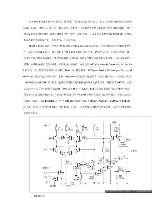
555 定时器的内部电路框图和外引脚排列图分别如图2.9.1 和图2.9.2 所示。
它内部包括两个电压比较器,三个等值串联电阻,一个RS 触发器,一个放电管T 及功率输出级。
它提供两个基准电压VCC /3 和2VCC /3 555 定时器的功能主要由两个比较器决定。
两个比较器的输出电压控制RS 触发器和放电管的状态。
在电源与地之间加上电压,当5 脚悬空时,则电压比较器C1 的同相输入端的电压为2VCC /3,C2 的反相输入端的电压为VCC /3。
若触发输入端TR 的电压小于VCC /3,则比较器C2 的输出为0,可使RS 触发器置1,使输出端OUT=1。
如果阈值输入端TH 的电压大于2VCC/3,同时TR 端的电压大于VCC /3,则C1 的输出为0,C2 的输出为1,可将RS 触发器置0,使输出为0 电平。
它的各个引脚功能如下:1脚:外接电源负端VSS或接地,一般情况下接地。
8脚:外接电源VCC,双极型时基电路VCC的范围是4.5 ~ 16V,CMOS型时基电路VCC的范围为3 ~ 18V。
一般用5V。
3脚:输出端Vo2脚:低触发端6脚:TH高触发端4脚:是直接清零端。
当端接低电平,则时基电路不工作,此时不论、TH处于何电平,时基电路输出为“0”,该端不用时应接高电平。
5脚:VC为控制电压端。
若此端外接电压,则可改变内部两个比较器的基准电压,当该端不用时,应将该端串入一只0.01μF电容接地,以防引入干扰。
7脚:放电端。
该端与放电管集电极相连,用做定时器时电容的放电。
在1脚接地,5脚未外接电压,两个比较器A1、A2基准电压分别为的情况下,555时基电路的功能表如表6—1示。
表6—1 555定时器的功能表清零端高触发端TH 低触发端Q 放电管T 功能0 0 导通直接清零××1 0 1 x 保持上一状态保持上一状态1 1 0 x 保持上一状态保持上一状态1 0111导通截止置1清零。
FEATURESDESCRIPTION/ORDERING INFORMATION12348765GNDTRIGOUTRESETVCCDISCHTHRESCONT3212019910111213456781817161514NCDISCHNCTHRESNCNCTRIGNCOUTNCNCGNDNCCONTNCVCCNCNCRESETNCNC – No internal connectionNA555...D OR P PACKAGENE555...D,P,PS,OR PW PACKAGESA555...D OR P PACKAGESE555...D,JG,OR P PACKAGE(TOP VIEW)SE555...FK PACKAGE(TOP VIEW)NA555,NE555,SA555,SE555PRECISION TIMERSSLFS022F–SEPTEMBER1973–REVISED JUNE2006•Timing From Microseconds to Hours•Adjustable Duty Cycle•Astable or Monostable Operation•TTL-Compatible Output Can Sink or Sourceup to200mAThese devices are precision timing circuits capable of producing accurate time delays or oscillation.In the time-delay or monostable mode of operation,the timed interval is controlled by a single external resistor and capacitor network.In the astable mode of operation,the frequency and duty cycle can be controlled independently with two external resistors and a single external capacitor.The threshold and trigger levels normally are two-thirds and one-third,respectively,of V CC.These levels can be altered by use of the control-voltage terminal.When the trigger input falls below the trigger level,the flip-flop is set,and the output goes high.If the trigger input is above the trigger level and the threshold input is above the threshold level,the flip-flop is reset and the output is low.The reset(RESET)input can override all other inputs and can be used to initiate a new timing cycle.When RESET goes low,the flip-flop is reset,and the output goes low.When the output is low,a low-impedance path is provided between discharge(DISCH)and ground.The output circuit is capable of sinking or sourcing current up to200mA.Operation is specified for supplies of 5V to15V.With a5-V supply,output levels are compatible with TTL inputs.Please be aware that an important notice concerning availability,standard warranty,and use in critical applications of TexasInstruments semiconductor products and disclaimers thereto appears at the end of this data sheet.PRODUCTION DATA information is current as of publication date.Copyright©1973–2006,Texas Instruments Incorporated Products conform to specifications per the terms of the Texas On products compliant to MIL-PRF-38535,all parameters are Instruments standard warranty.Production processing does not tested unless otherwise noted.On all other products,production necessarily include testing of all parameters.processing does not necessarily include testing of all parameters.NA555,NE555,SA555,SE555PRECISION TIMERSSLFS022F–SEPTEMBER 1973–REVISED JUNE 2006ORDERING INFORMATIONV THRES T AMAX PACKAGE (1)ORDERABLE PART NUMBER TOP-SIDE MARKING V CC =15VPDIP –P Tube of 50NE555P NE555P Tube of 75NE555D SOIC –DNE555Reel of 2500NE555DR 0°C to 70°C11.2VSOP –PS Reel of 2000NE555PSR N555Tube of 150NE555PW TSSOP –PW N555Reel of 2000NE555PWR PDIP –PTube of 50SA555P SA555P –40°C to 85°C11.2VTube of 75SA555D SOIC –D SA555Reel of 2000SA555DR PDIP –PTube of 50NA555P NA555P –40°C to 105°C11.2VTube of 75NA555D SOIC –D NA555Reel of 2000NA555DR PDIP –PTube of 50SE555P SE555P Tube of 75SE555D SOIC –D SE555D –55°C to 125°C10.6Reel of 2500SE555DR CDIP –JG Tube of 50SE555JG SE555JG LCCC –FKTube of 55SE555FKSE555FK(1)Package drawings,standard packing quantities,thermal data,symbolization,and PCB design guidelines are available at /sc/package.FUNCTION TABLETRIGGER THRESHOLD DISCHARGE RESET OUTPUT VOLTAGE (1)VOLTAGE (1)SWITCHLow Irrelevant Irrelevant Low On High <1/3V DD Irrelevant High Off High >1/3V DD >2/3V DD LowOnHigh>1/3V DD<2/3V DDAs previously established(1)Voltage levels shown are nominal.2Submit Documentation FeedbackTRIGTHRESOUTDISCHPin numbers shown are for the D, JG, P , PS, and PW packages.NOTE A:RESET can override TRIG, which can override THRES.NA555,NE555,SA555,SE555PRECISION TIMERSSLFS022F–SEPTEMBER 1973–REVISED JUNE 2006FUNCTIONAL BLOCK DIAGRAM3Submit Documentation FeedbackAbsolute Maximum Ratings (1)Recommended Operating ConditionsNA555,NE555,SA555,SE555PRECISION TIMERSSLFS022F–SEPTEMBER 1973–REVISED JUNE 2006over operating free-air temperature range (unless otherwise noted)MINMAX UNIT V CC Supply voltage (2)18V V I Input voltage CONT,RESET,THRES,TRIGV CC V I OOutput current±225mAD package97P package 85θJAPackage thermal impedance (3)(4)°C/W PS package 95PW package149FK package 5.61θJC Package thermal impedance (5)(6)°C/W JG package14.5T JOperating virtual junction temperature 150°C Case temperature for 60sFK package 260°C Lead temperature 1,6mm (1/16in)from case for 60sJG package300°C T stg Storage temperature range–65150°C (1)Stresses beyond those listed under "absolute maximum ratings"may cause permanent damage to the device.These are stress ratings only,and functional operation of the device at these or any other conditions beyond those indicated under "recommended operating conditions"is not implied.Exposure to absolute-maximum-rated conditions for extended periods may affect device reliability.(2)All voltage values are with respect to GND.(3)Maximum power dissipation is a function of T J (max),θJA ,and T A .The maximum allowable power dissipation at any allowable ambient temperature is P D =(T J (max)-T A )/θJA.Operating at the absolute maximum T J of 150°C can affect reliability.(4)The package thermal impedance is calculated in accordance with JESD 51-7.(5)Maximum power dissipation is a function of T J (max),θJC ,and T C .The maximum allowable power dissipation at any allowable case temperature is P D =(T J (max)-T C )/θJC .Operating at the absolute maximum T J of 150°C can affect reliability.(6)The package thermal impedance is calculated in accordance with MIL-STD-883.over operating free-air temperature range (unless otherwise noted)MINMAX UNIT NA555,NE555,SA555 4.516V CC Supply voltage V SE5554.518V I Input voltage CONT,RESET,THRES,and TRIGV CC V I OOutput current±200mANA555–40105NE555070T AOperating free-air temperature°C SA555–4085SE555–551254Submit Documentation FeedbackElectrical CharacteristicsNA555,NE555,SA555,SE555PRECISION TIMERS SLFS022F–SEPTEMBER1973–REVISED JUNE2006V CC =5V to15V,TA=25°C(unless otherwise noted)NA555SE555NE555PARAMETER TEST CONDITIONS UNITSA555MIN TYP MAX MIN TYP MAX V CC=15V9.41010.68.81011.2THRES voltage level V V CC=5V 2.7 3.34 2.4 3.3 4.2THRES current(1)3025030250nA4.855.2 4.55 5.6V CC=15VT A=–55°C to125°C36TRIG voltage level V1.45 1.67 1.9 1.1 1.672.2V CC=5VT A=–55°C to125°C 1.9TRIG current TRIG at0V0.50.90.52µA0.30.710.30.71RESET voltage level V T A=–55°C to125°C 1.1RESET at V CC0.10.40.10.4RESET current mA RESET at0V–0.4–1–0.4–1.5DISCH switch off-state2010020100nA current9.61010.491011V CC=15VT A=–55°C to125°C9.610.4CONT voltageV (open circuit) 2.9 3.3 3.8 2.6 3.34V CC=5VT A=–55°C to125°C 2.9 3.80.10.150.10.25V CC=15V,I OL=10mAT A=–55°C to125°C0.20.40.50.40.75V CC=15V,I OL=50mAT A=–55°C to125°C12 2.22 2.5V CC=15V,I OL=100mALow-level output voltage T A=–55°C to125°C 2.7VV CC=15V,I OL=200mA 2.5 2.5V CC=5V,I OL=3.5mA T A=–55°C to125°C0.350.10.20.10.35V CC=5V,I OL=5mAT A=–55°C to125°C0.8V CC=5V,I OL=8mA0.150.250.150.41313.312.7513.3V CC=15V,I OL=–100mAT A=–55°C to125°C12High-level output voltage V CC=15V,I OH=–200mA12.512.5V3 3.3 2.75 3.3V CC=15V,I OL=–100mAT A=–55°C to125°C2V CC=15V10121015Output low,No loadV CC=5V3536Supply current mAV CC=15V910913Output high,No loadV CC=5V2425(1)This parameter influences the maximum value of the timing resistors R A and R B in the circuit of Figure12.For example,when V CC=5V,the maximum value is R=R A+R B≈3.4MΩ,and for V CC=15V,the maximum value is10MΩ.5Submit Documentation FeedbackOperating CharacteristicsNA555,NE555,SA555,SE555PRECISION TIMERSSLFS022F–SEPTEMBER 1973–REVISED JUNE 2006V CC =5V to 15V,T A =25°C (unless otherwise noted)NA555SE555NE555TESTPARAMETERUNITSA555CONDITIONS (1)MINTYP MAX MINTYP MAXEach timer,monostable (3)T A =25°C0.5 1.5(4)13Initial error of timing %interval (2)Each timer,astable (5) 1.5 2.25Each timer,monostable (3)T A =MIN to MAX 30100(4)50Temperature coefficient of ppm/timing interval°C Each timer,astable (5)90150Each timer,monostable (3)T A =25°C 0.050.2(4)0.10.5Supply-voltage sensitivity of %/V timing interval Each timer,astable (5)0.150.3C L =15pF,Output-pulse rise time 100200(4)100300ns T A =25°C C L =15pF,Output-pulse fall time 100200(4)100300ns T A =25°C (1)For conditions shown as MIN or MAX,use the appropriate value specified under recommended operating conditions.(2)Timing interval error is defined as the difference between the measured value and the average value of a random sample from each process run.(3)Values specified are for a device in a monostable circuit similar to Figure 9,with the following component values:R A =2k Ωto 100k Ω,C =0.1µF.(4)On products compliant to MIL-PRF-38535,this parameter is not production tested.(5)Values specified are for a device in an astable circuit similar to Figure 12,with the following component values:R A =1k Ωto 100k Ω,C =0.1µF.6Submit Documentation FeedbackTYPICAL CHARACTERISTICSI OL − Low-Level Output Current − mALOW-LEVEL OUTPUT VOLTAGEvsLOW-LEVEL OUTPUT CURRENT− L o w -L e v e l O u t p u t V o l t a g e − VV O LLOW-LEVEL OUTPUT VOLTAGEvsLOW-LEVEL OUTPUT CURRENT− L o w -L e v e l O u t p u t V o l t a g e − VV O L I OL − Low-Level Output Current − mA0.020.22LOW-LEVEL OUTPUT VOLTAGEvsLOW-LEVEL OUTPUT CURRENT− L o w -L e v e l O u t p u t V o l t a g e− VV O L I OL − Low-Level Output Current − mA 10.60.201.41.82.00.41.60.81.2− I OH − High-Level Output Current − mAV C C V O H − V o l t a g e D r o p − V)(DROP BETWEEN SUPPLY VOLTAGE AND OUTPUTvsHIGH-LEVEL OUTPUT CURRENTNA555,NE555,SA555,SE555PRECISION TIMERSSLFS022F–SEPTEMBER 1973–REVISED JUNE 2006Data for temperatures below 0°C and above 70°C are applicable for SE555circuits only.Figure 1.Figure 2.Figure 3.Figure 4.7Submit Documentation Feedback567891011− S u p p l y C u r r e n t − m ASUPPLY CURRENTvsSUPPLY VOLTAGE12131415C C I V CC − Supply Voltage − V10.9950.9900.9855101.0051.010NORMALIZED OUTPUT PULSE DURATION(MONOSTABLE OPERATION)vsSUPPLY VOLTAGE1.0151520C CV P u l s e D u r a t i o nR e l a t i v e t o V a l u e a t = 10 V V CC − Supply Voltage − V−75−2525NORMALIZED OUTPUT PULSE DURATION(MONOSTABLE OPERATION)vsFREE-AIR TEMPERATURE75125T A − Free-Air Temperature − °C−5050100P u l s e D u r a t i o n R e l a t i v e t o V a l u e a t T A = 255C− P r o p a g a t i o n D e l a y T i m e − n sPROPAGATION DELAY TIMEvsLOWEST VOLTAGE LEVEL OF TRIGGER PULSELowest Voltage Level of Trigger Pulset P D 00.1 x V CC0.2 x V CC0.3 x V CC0.4 x V CCNA555,NE555,SA555,SE555PRECISION TIMERSSLFS022F–SEPTEMBER 1973–REVISED JUNE 2006TYPICAL CHARACTERISTICS (continued)Data for temperatures below 0°C and above 70°C are applicable for SE555circuits only.Figure 5.Figure 6.Figure 7.Figure 8.8Submit Documentation FeedbackAPPLICATION INFORMATIONMonostable OperationV CC(5 V to 15 V)OutputInputPin numbers shown are for the D, JG, P , PS, and PW packages.NA555,NE555,SA555,SE555PRECISION TIMERSSLFS022F–SEPTEMBER 1973–REVISED JUNE 2006For monostable operation,any of these timers can be connected as shown in Figure 9.If the output is low,application of a negative-going pulse to the trigger (TRIG)sets the flip-flop (Q goes low),drives the output high,and turns off Q1.Capacitor C then is charged through R A until the voltage across the capacitor reaches the threshold voltage of the threshold (THRES)input.If TRIG has returned to a high level,the output of the threshold comparator resets the flip-flop (Q goes high),drives the output low,and discharges C through Q1.Figure 9.Circuit for Monostable OperationMonostable operation is initiated when TRIG voltage falls below the trigger threshold.Once initiated,the sequence ends only if TRIG is high at the end of the timing interval.Because of the threshold level and saturation voltage of Q1,the output pulse duration is approximately t w =1.1R A C.Figure 11is a plot of the time constant for various values of R A and C.The threshold levels and charge rates both are directly proportional to the supply voltage,V CC .The timing interval is,therefore,independent of the supply voltage,so long as the supply voltage is constant during the time interval.Applying a negative-going trigger pulse simultaneously to RESET and TRIG during the timing interval discharges C and reinitiates the cycle,commencing on the positive edge of the reset pulse.The output is held low as long as the reset pulse is low.To prevent false triggering,when RESET is not used,it should be connected to V CC .9Submit Documentation Feedback− O u t p u t P u l s e D u r a t i o n − sC − Capacitance − µF10110−110−210−310−410−5t w V o l t a g e − 2 V /d i vTime − 0.1 ms/divAstable OperationV o l t a g e − 1 V /d i vTime − 0.5 ms/divttR R OutputL V CCNOTE A:Decoupling CONT voltage to ground with a capacitor canimprove operation. This should be evaluated for individual applications.Pin numbers shown are for the D, JG, P , PS, and PW packages.NA555,NE555,SA555,SE555PRECISION TIMERSSLFS022F–SEPTEMBER 1973–REVISED JUNE 2006APPLICATION INFORMATION (continued)Figure 10.Typical Monostable Waveforms Figure 11.Output Pulse Duration vs CapacitanceAs shown in Figure 12,adding a second resistor,R B ,to the circuit of Figure 9and connecting the trigger input to the threshold input causes the timer to self-trigger and run as a multivibrator.The capacitor C charges through R A and R B and then discharges through R B only.Therefore,the duty cycle is controlled by the values of R A and R B .This astable connection results in capacitor C charging and discharging between the threshold-voltage level (≈0.67×V CC )and the trigger-voltage level (≈0.33×V CC ).As in the monostable circuit,charge and discharge times (and,therefore,the frequency and duty cycle)are independent of the supply voltage.Figure 12.Circuit for Astable Operation Figure 13.Typical Astable Waveforms10Submit Documentation FeedbacktH+0.693(R A )R B)Ct L +0.693(R B)C Other useful relationships are shown below.period +t H )t L +0.693(R A )2R B)Cfrequency [1.44(R A )2R B )C Output driver duty cycle +tL t H )t L +RB R A )2R B Output waveform duty cycle+t L t H +R B R A )R BLow-to-high ratio +t H t H )t L +1–R B R A )2R Bf − F r e e -R u n n i ng F r e q u e n c y − H zC − Capacitance − µF1001010.10.010.001Missing-PulseDetectorTime − 0.1 ms/divV o l t a g e − 2 V /d i vPin numbers shown are shown for the D, JG, P , PS, and PW packages.NA555,NE555,SA555,SE555PRECISION TIMERSSLFS022F–SEPTEMBER 1973–REVISED JUNE 2006APPLICATION INFORMATION (continued)Figure 13shows typical waveforms generated during astable operation.The output high-level duration t H and low-level duration t L can be calculated as follows:Figure 14.Free-Running FrequencyThe circuit shown in Figure 15can be used to detect a missing pulse or abnormally long spacing between consecutive pulses in a train of pulses.The timing interval of the monostable circuit is retriggered continuously by the input pulse train as long as the pulse spacing is less than the timing interval.A longer pulse spacing,missing pulse,or terminated pulse train permits the timing interval to be completed,thereby generating an output pulse as shown in Figure 16.Figure 15.Circuit for Missing-Pulse DetectorFigure pleted Timing Waveforms forMissing-Pulse DetectorFrequency DividerV o l t a g e − 2 V /d i vTime − 0.1 ms/divNA555,NE555,SA555,SE555PRECISION TIMERSSLFS022F–SEPTEMBER 1973–REVISED JUNE 2006APPLICATION INFORMATION (continued)By adjusting the length of the timing cycle,the basic circuit of Figure 9can be made to operate as a frequency divider.Figure 17shows a divide-by-three circuit that makes use of the fact that retriggering cannot occur during the timing cycle.Figure 17.Divide-by-Three Circuit WaveformsPulse-Width ModulationCAV (5 V to 15 V)OutputModulationInput(see Note A)Clock InputNOTE A:The modulating signal can be direct or capacitively coupledto CONT . For direct coupling, the effects of modulation source voltage and impedance on the bias of the timer should be considered.Pin numbers shown are for the D, JG, P , PS, and PW packages.V o l t a g e − 2 V /d i vTime − 0.5 ms/divNA555,NE555,SA555,SE555PRECISION TIMERSSLFS022F–SEPTEMBER 1973–REVISED JUNE 2006APPLICATION INFORMATION (continued)The operation of the timer can be modified by modulating the internal threshold and trigger voltages,which is accomplished by applying an external voltage (or current)to CONT.Figure 18shows a circuit for pulse-width modulation.A continuous input pulse train triggers the monostable circuit,and a control signal modulates the threshold voltage.Figure 19shows the resulting output pulse-width modulation.While a sine-wave modulation signal is shown,any wave shape could be used.Figure 18.Circuit for Pulse-Width Modulation Figure 19.Pulse-Width-Modulation WaveformsPulse-Position ModulationV o l t a g e − 2 V /d i vTime − 0.1 ms/divNOTE A:The modulating signal can be direct or capacitively coupledto CONT . For direct coupling, the effects of modulation source voltage and impedance on the bias of the timer should be considered.Pin numbers shown are for the D, JG, P , PS, and PW packages.OutputNA555,NE555,SA555,SE555PRECISION TIMERSSLFS022F–SEPTEMBER 1973–REVISED JUNE 2006APPLICATION INFORMATION (continued)As shown in Figure 20,any of these timers can be used as a pulse-position modulator.This application modulates the threshold voltage and,thereby,the time delay,of a free-running oscillator.Figure 21shows a triangular-wave modulation signal for such a circuit;however,any wave shape could be used.Figure 20.Circuit for Pulse-Position Modulation Figure 21.Pulse-Position-Modulation WaveformsSequential TimerC B = 4.7 µF R B = 100 k ΩPin numbers shown are for the D, JG, P , PS, and PW packages.NOTE A:S closes momentarily at t = 0.V o l t a g e − 5 V /d i vt − Time − 1 s/divNA555,NE555,SA555,SE555PRECISION TIMERSSLFS022F–SEPTEMBER 1973–REVISED JUNE 2006APPLICATION INFORMATION (continued)Many applications,such as computers,require signals for initializing conditions during start-up.Other applications,such as test equipment,require activation of test signals in sequence.These timing circuits can be connected to provide such sequential control.The timers can be used in various combinations of astable or monostable circuit connections,with or without modulation,for extremely flexible waveform control.Figure 22shows a sequencer circuit with possible applications in many systems,and Figure 23shows the output waveforms.Figure 22.Sequential Timer CircuitFigure 23.Sequential Timer WaveformsPACKAGING INFORMATIONOrderableDevice Status (1)Package Type Package Drawing Pins Package Qty Eco Plan (2)Lead/Ball Finish MSL Peak Temp (3)JM38510/10901BPAACTIVE CDIP JG 81TBD A42SNPB N /A for Pkg Type NA555D ACTIVE SOIC D 875Green (RoHS &no Sb/Br)CU NIPDAU Level-1-260C-UNLIM NA555DG4ACTIVE SOIC D 875Green (RoHS &no Sb/Br)CU NIPDAU Level-1-260C-UNLIM NA555DR ACTIVE SOIC D 82500Green (RoHS &no Sb/Br)CU NIPDAU Level-1-260C-UNLIM NA555DRG4ACTIVE SOIC D 82500Green (RoHS &no Sb/Br)CU NIPDAU Level-1-260C-UNLIM NA555P ACTIVE PDIP P 850Pb-Free (RoHS)CU NIPDAU N /A for Pkg Type NA555PE4ACTIVE PDIP P 850Pb-Free (RoHS)CU NIPDAU N /A for Pkg Type NE555D ACTIVE SOIC D 875Green (RoHS &no Sb/Br)CU NIPDAU Level-1-260C-UNLIM NE555DE4ACTIVE SOIC D 875Green (RoHS &no Sb/Br)CU NIPDAU Level-1-260C-UNLIM NE555DG4ACTIVE SOIC D 875Green (RoHS &no Sb/Br)CU NIPDAU Level-1-260C-UNLIM NE555DR ACTIVE SOIC D 82500Green (RoHS &no Sb/Br)CU NIPDAU Level-1-260C-UNLIM NE555DRE4ACTIVE SOIC D 82500Green (RoHS &no Sb/Br)CU NIPDAU Level-1-260C-UNLIM NE555DRG4ACTIVE SOIC D 82500Green (RoHS &no Sb/Br)CU NIPDAU Level-1-260C-UNLIM NE555P ACTIVE PDIP P 850Pb-Free (RoHS)CU NIPDAU N /A for Pkg Type NE555PE4ACTIVE PDIP P 850Pb-Free (RoHS)CU NIPDAU N /A for Pkg Type NE555PSLE OBSOLETE SO PS 8TBDCall TI Call TINE555PSR ACTIVE SO PS 82000Green (RoHS &no Sb/Br)CU NIPDAU Level-1-260C-UNLIM NE555PSRE4ACTIVE SO PS 82000Green (RoHS &no Sb/Br)CU NIPDAU Level-1-260C-UNLIM NE555PW ACTIVE TSSOP PW 8150Green (RoHS &no Sb/Br)CU NIPDAU Level-1-260C-UNLIM NE555PWE4ACTIVE TSSOP PW 8150Green (RoHS &no Sb/Br)CU NIPDAU Level-1-260C-UNLIM NE555PWR ACTIVE TSSOP PW 82000Green (RoHS &no Sb/Br)CU NIPDAU Level-1-260C-UNLIM NE555PWRE4ACTIVE TSSOPPW82000Green (RoHS &no Sb/Br)CU NIPDAU Level-1-260C-UNLIM NE555Y OBSOLETE 0TBD Call TI Call TISA555D ACTIVE SOIC D 875Green (RoHS &no Sb/Br)CU NIPDAU Level-1-260C-UNLIM SA555DE4ACTIVE SOIC D 875Green (RoHS &no Sb/Br)CU NIPDAU Level-1-260C-UNLIM SA555DG4ACTIVESOICD875Green (RoHS &no Sb/Br)CU NIPDAULevel-1-260C-UNLIM31-Jul-2006Orderable DeviceStatus (1)Package Type Package DrawingPins Package Qty Eco Plan (2)Lead/Ball Finish MSL Peak Temp (3)SA555DR ACTIVE SOIC D 82500Green (RoHS &no Sb/Br)CU NIPDAU Level-1-260C-UNLIM SA555DRE4ACTIVE SOIC D 82500Green (RoHS &no Sb/Br)CU NIPDAU Level-1-260C-UNLIM SA555DRG4ACTIVE SOIC D 82500Green (RoHS &no Sb/Br)CU NIPDAU Level-1-260C-UNLIM SA555P ACTIVE PDIP P 850Pb-Free (RoHS)CU NIPDAU N /A for Pkg Type SA555PE4ACTIVE PDIP P 850Pb-Free (RoHS)CU NIPDAU N /A for Pkg Type SE555D ACTIVE SOIC D 875TBD CU NIPDAU Level-1-220C-UNLIM SE555DR ACTIVE SOIC D 82500TBD CU NIPDAU Level-1-220C-UNLIM SE555FKB ACTIVE LCCC FK 201TBD POST-PLATE N /A for Pkg TypeSE555JG ACTIVE CDIP JG 81TBD A42SNPB N /A for Pkg Type SE555JGB ACTIVE CDIP JG 81TBD A42SNPB N /A for Pkg Type SE555N OBSOLETE PDIP N 8TBD Call TI Call TISE555PACTIVEPDIPP850Pb-Free (RoHS)CU NIPDAUN /A for Pkg Type(1)The marketing status values are defined as follows:ACTIVE:Product device recommended for new designs.LIFEBUY:TI has announced that the device will be discontinued,and a lifetime-buy period is in effect.NRND:Not recommended for new designs.Device is in production to support existing customers,but TI does not recommend using this part in a new design.PREVIEW:Device has been announced but is not in production.Samples may or may not be available.OBSOLETE:TI has discontinued the production of the device.(2)Eco Plan -The planned eco-friendly classification:Pb-Free (RoHS),Pb-Free (RoHS Exempt),or Green (RoHS &no Sb/Br)-please check /productcontent for the latest availability information and additional product content details.TBD:The Pb-Free/Green conversion plan has not been defined.Pb-Free (RoHS):TI's terms "Lead-Free"or "Pb-Free"mean semiconductor products that are compatible with the current RoHS requirements for all 6substances,including the requirement that lead not exceed 0.1%by weight in homogeneous materials.Where designed to be soldered at high temperatures,TI Pb-Free products are suitable for use in specified lead-free processes.Pb-Free (RoHS Exempt):This component has a RoHS exemption for either 1)lead-based flip-chip solder bumps used between the die and package,or 2)lead-based die adhesive used between the die and leadframe.The component is otherwise considered Pb-Free (RoHS compatible)as defined above.Green (RoHS &no Sb/Br):TI defines "Green"to mean Pb-Free (RoHS compatible),and free of Bromine (Br)and Antimony (Sb)based flame retardants (Br or Sb do not exceed 0.1%by weight in homogeneous material)(3)MSL,Peak Temp.--The Moisture Sensitivity Level rating according to the JEDEC industry standard classifications,and peak solder temperature.Important Information and Disclaimer:The information provided on this page represents TI's knowledge and belief as of the date that it is provided.TI bases its knowledge and belief on information provided by third parties,and makes no representation or warranty as to the accuracy of such information.Efforts are underway to better integrate information from third parties.TI has taken and continues to take reasonable steps to provide representative and accurate information but may not have conducted destructive testing or chemical analysis on incoming materials and chemicals.TI and TI suppliers consider certain information to be proprietary,and thus CAS numbers and other limited information may not be available for release.In no event shall TI's liability arising out of such information exceed the total purchase price of the TI part(s)at issue in this document sold by TI to Customer on an annual basis.31-Jul-2006IMPORTANT NOTICETexas Instruments Incorporated and its subsidiaries (TI) reserve the right to make corrections, modifications, enhancements, improvements, and other changes to its products and services at any time and to discontinue any product or service without notice. Customers should obtain the latest relevant information before placing orders and should verify that such information is current and complete. All products are sold subject to TI’s terms and conditions of sale supplied at the time of order acknowledgment.TI warrants performance of its hardware products to the specifications applicable at the time of sale in accordance with TI’s standard warranty. T esting and other quality control techniques are used to the extent TI deems necessary to support this warranty. Except where mandated by government requirements, testing of all parameters of each product is not necessarily performed.TI assumes no liability for applications assistance or customer product design. Customers are responsible for their products and applications using TI components. T o minimize the risks associated with customer products and applications, customers should provide adequate design and operating safeguards.TI does not warrant or represent that any license, either express or implied, is granted under any TI patent right, copyright, mask work right, or other TI intellectual property right relating to any combination, machine, or process in which TI products or services are used. Information published by TI regarding third-party products or services does not constitute a license from TI to use such products or services or a warranty or endorsement thereof. Use of such information may require a license from a third party under the patents or other intellectual property of the third party, or a license from TI under the patents or other intellectual property of TI.Reproduction of information in TI data books or data sheets is permissible only if reproduction is without alteration and is accompanied by all associated warranties, conditions, limitations, and notices. Reproduction of this information with alteration is an unfair and deceptive business practice. TI is not responsible or liable for such altered documentation.Resale of TI products or services with statements different from or beyond the parameters stated by TI for that product or service voids all express and any implied warranties for the associated TI product or service and is an unfair and deceptive business practice. TI is not responsible or liable for any such statements. Following are URLs where you can obtain information on other Texas Instruments products and application solutions:Products ApplicationsAmplifiers Audio /audioData Converters Automotive /automotiveDSP Broadband /broadbandInterface Digital Control /digitalcontrolLogic Military /militaryPower Mgmt Optical Networking /opticalnetwork Microcontrollers Security /securityLow Power Wireless /lpw Telephony /telephonyVideo & Imaging /videoWireless /wirelessMailing Address:Texas InstrumentsPost Office Box 655303 Dallas, Texas 75265Copyright 2006, Texas Instruments Incorporated。