ZXTN25020DZTA;中文规格书,Datasheet资料
- 格式:pdf
- 大小:408.62 KB
- 文档页数:9

S E M I C O N D U C T O R SSUMMARYBV CEO = 100V :R SAT = 31m ; I C = 4.5A DESCRIPTIONPackaged in the SOT89outline this new low saturation 100V NPN transistor offers extremely low on state losses making it ideal for use in DC-DC circuits and various driving and power management functions.FEATURES• 4.5 amps continuous current •Up to 10 amps peak current •Very low saturation voltagesAPPLICATIONS•Motor driving •Line switching •High side switches•Subscriber line interface cards (SLIC)DEVICE MARKING853ZXTN2011ZISSUE 2 - MAY 2006100V NPN LOW SATURATION MEDIUM POWER TRANSISTOR IN SOT891SOT89PINOUTVIEWDEVICE REEL SIZE TAPE WIDTH QUANTITY PERREEL ZXTN2011ZTA7"12mm embossed1,000 unitsORDERING INFORMATIONZXTN2011ZS E M I C O N D U C T O R SISSUE 2 - MAY 2006 2PARAMETER SYMBOL LIMIT UNIT Collector base voltage BV CBO200V Collector emitter voltage BV CEO100V Emitter base voltage BV EBO7V Continuous collector current(a)I C 4.5A Peak pulse current I CM10APower dissipation at T A=25°C(a) Linear derating factor P D 1.512WmW/°CPower dissipation at T A=25°C(b) Linear derating factor P D 2.116.8WmW/°COperating and storage temperature range T j,T stg-55 to +150°C ABSOLUTE MAXIMUM RATINGSPARAMETER SYMBOL LIMIT UNIT Junction to ambient(a)RJA83°C/W Junction to ambient(b)RJA60°C/WNOTES:(a)For a device surface mounted on 25mm x 25mm x 1.6mm FR4 PCB with high coverage of single sided 1oz copper, in still air conditions.(b)For a device surface mounted on 50mm x 50mm x 1.6mm FR4 PCB with high coverage of single sided 1oz copper, in still air conditions. THERMAL RESISTANCEZXTN2011ZS E M I C O N D U C T O R SISSUE 2 - MAY 20063ZXTN2011ZS E M I C O N D U C T O R SISSUE 2 - MAY 2006 4PARAMETER SYMBOL MIN.TYP.MAX.UNIT CONDITIONS Collector base breakdown voltage BV CBO200235V I C=100A Collector emitter breakdown voltage BV CER200235V I C=1A,RBՅ1k⍀Collector emitter breakdown voltage BV CEO100115V I C=10mA*Emitter base breakdown voltage BV EBO78.1V I E=100ACollector cut-off current I CBO500.5nAAV CB=150VV CB=150V,T amb=100ЊCCollector cut-off current I CERRՅ1k⍀1000.5nAAV CB=150VV CB=150V,T amb=100ЊCEmitter cut-off current I EBO10nA V EB=6VCollector-emitter saturation voltage V CE(SAT)2045851553060115195mVmVmVmVI C=0.1A,I B=5mA*I C=1A,I B=100mA*I C=2A,I B=100mA*I C=5A,I B=500mA*Base emitter saturation voltage V BE(SAT)10001100mV I C=5A,I B=500mA* Base emitter turn on voltage V BE(ON)9001000mV I C=5A,V CE=2V*Static forward current transfer ratio h FE10010030102302006020300I C=10mA,V CE=2V*I C=2A,V CE=2V*I C=5A,V CE=2V*I C=10A,V CE=2V*Transition frequency f T130MHz I C=100mA,V CE=10Vf=50MHzOutput capacitance C OBO26pF V CB=10V,f=1MHz*Switching times t ONt OFF411010ns I C=1A,V CC=10V,I B1=I B2=100mAELECTRICAL CHARACTERISTICS(at T amb= 25°C unless otherwise stated) * Measured under pulsed conditions. Pulse widthՅ300s; duty cycleՅ2%.ZXTN2011ZS E M I C O N D U C T O R SISSUE 2 - MAY 20065ZXTN2011ZS E M I C O N D U C T O R S6ISSUE 2 - MAY 2006EuropeZetex GmbHStreitfeldstraße 19D-81673 München GermanyTelefon: (49) 89 45 49 49 0Fax: (49) 89 45 49 49 49europe.sales@AmericasZetex Inc700 Veterans Memorial Hwy Hauppauge, NY 11788USATelephone: (1) 631 360 2222Fax: (1) 631 360 8222usa.sales@Asia PacificZetex (Asia) Ltd3701-04Metroplaza Tower 1Hing Fong Road, Kwai Fong Hong KongTelephone: (852) 26100 611Fax: (852) 24250 494asia.sales@Corporate Headquarters Zetex Semiconductors plc Zetex Technology ParkChadderton, Oldham, OL9 9LL United KingdomTelephone (44) 161 622 4444Fax: (44) 161 622 4446hq@These offices are supported by agents and distributors in major countries world-wide.This publication is issued to provide outline information only which (unless agreed by the Company in writing)may not be used,applied or reproduced for any purpose or form part of any order or contract or be regarded as a representation relating to the products or services concerned.The Company reserves the right to alter without notice the specification, design, price or conditions of supply of any product or service.For the latest product information,log on to ©ZetexSemiconductors plc 2005。

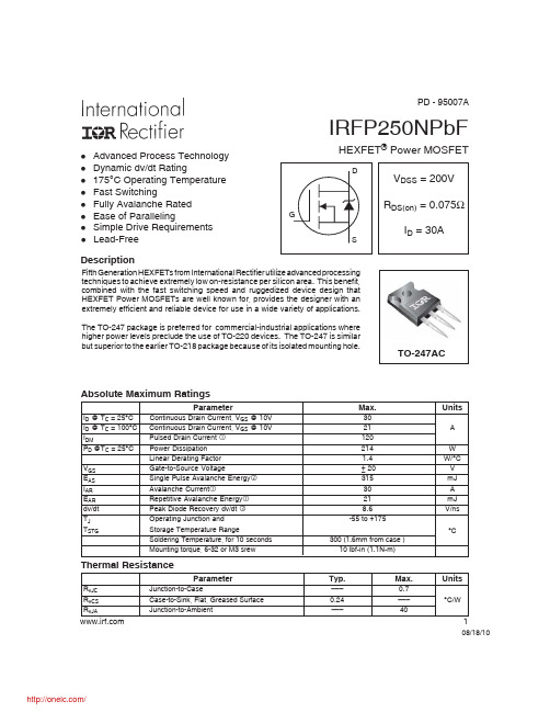
IRFP250NPbFHEXFET ® Power MOSFET08/18/10ParameterMax.UnitsI D @ T C = 25°C Continuous Drain Current, V GS @ 10V 30I D @ T C = 100°C Continuous Drain Current, V GS @ 10V 21A I DMPulsed Drain Current 120P D @T C = 25°C Power Dissipation 214W Linear Derating Factor 1.4W/°C V GS Gate-to-Source Voltage± 20V E AS Single Pulse Avalanche Energy 315mJ I AR Avalanche Current30A E AR Repetitive Avalanche Energy 21mJ dv/dt Peak Diode Recovery dv/dt 8.6V/ns T J Operating Junction and-55 to +175T STGStorage Temperature RangeSoldering Temperature, for 10 seconds 300 (1.6mm from case )°CMounting torque, 6-32 or M3 srew10 lbf•in (1.1N•m)Absolute Maximum RatingsParameterTyp.Max.UnitsR θJC Junction-to-Case–––0.7R θCS Case-to-Sink, Flat, Greased Surface 0.24–––°C/WR θJAJunction-to-Ambient–––40Thermal Resistance 1Descriptionl Advanced Process Technology l Dynamic dv/dt Ratingl 175°C Operating Temperature l Fast Switchingl Fully Avalanche Rated l Ease of Parallelingl Simple Drive Requirements TO-247AClLead-FreePD - 95007AIRFP250NPbFSource-Drain Ratings and CharacteristicsStarting T J = 25°C, L = 1.9mHR G = 25Ω, I AS = 18A. (See Figure 12)Repetitive rating; pulse width limited by max. junction temperature. (See Fig. 11)Notes:I SD ≤ 18A , di/d t ≤ 374A/µs, V DD ≤ V (BR)DSS ,T J ≤ 175°CPulse width ≤ 300µs; duty cycle ≤ 2%.Electrical Characteristics @ T = 25°C (unless otherwise specified)IRFP250NPbF 3Vs. TemperatureIRFP250NPbF4Fig 5. Typical Capacitance Vs.Drain-to-Source VoltageFig 6.Gate-to-Source VoltageForward VoltageTypical Gate Charge Vs.1101001000V DS , Drain-to-Source Voltage (V)010002000300040005000C , C a p a c i t a n c e (p F )IRFP250NPbF5Fig 9. Maximum Drain Current Vs.Fig 10a. Switching Time Test CircuitV V d(on)rd(off)fFig 10b. Switching Time WaveformsFig 11. Maximum Effective Transient Thermal Impedance, Junction-to-CaseDDIRFP250NPbF6VDSCurrent Sampling Resistors10 VFig 13b. Gate Charge Test CircuitFig 13a. Basic Gate Charge Waveform Fig 12b. Unclamped Inductive WaveformsI ASVs. Drain CurrentV DDIRFP250NPbF7Fig 14. For N-Channel HEXFETS* V GS = 5V for Logic Level DevicesPeak Diode Recovery dv/dt Test CircuitV DDIRFP250NPbFData and specifications subject to change without notice.233 Kansas St., El Segundo, California 90245, USA Tel: (310) 252-7105TAC Fax: (310) 252-7903Visit us at for sales contact information .08/2010分销商库存信息: IRIRFP250NPBF。


TransistorsRev.A 1/2General purpose (dual transistors)EMT2 / UMT2N / IMT2Az Features1) Two 2SA1037AK chips in a EMT or UMT or SMT package.z Equivalent circuitsz Absolute maximum ratings (T a=25°C)ParameterSymbol V CBO V CEO V EBO I CP C Tj TstgLimits −60−50−6−150300(TOTAL)150(TOTAL)EMT2 / UMT2N IMT2A150−55 to +150Unit V V V mA mW°C °CCollector-base voltage Collector-emitter voltage Emitter-base voltage Collector current Collector power dissipationJunction temperature Storage temperature∗1 120mW per element must not be exceeded.∗2 200mW per element must not be exceeded.∗1∗2z Package, marking, and packaging specificationsEMT2EMT6T2T2R 8000IMT2A SMT6T2T1083000UMT2N UMT6T2TR 3000Type Package Marking CodeBasic ordering unit (pieces)z External dimensions (Unit : mm)z Electrical characteristics (T a=25°C)ParameterSymbol Min.Typ.Max.Unit ConditionsTransition frequency BV CBO BV CEO BV EBO I CBO I EBO V CE(sat)h FE f T −60−50−6−−−120−−−−−−−−140−−−−0.1−0.1−0.5560−V V V µA µA V −MHz ∗Cob−45pFI C =−50µA I C =−1mA I E =−50µA V CB =−60V V EB =−6VV CE =−12V, I E =2mA, f =100MHz V CE =−12V, I E =0A, f =1MHzI C /I B =−50mA/−5mA V CE =−6V, I C =−1mA∗Transition frequency of the device.Collector-base breakdown voltage Collector-emitter breakdown voltage Emitter-base breakdown voltage Collector cutoff current Emitter cutoff currentCollector-emitter saturation voltage DC current transfer ratio Output capacitanceTransistors Rev.A 2/2z Electrical characteristics curvesFig.1 Grounded emitter propagationcharacteristics C O L L E C T O R C U R R E N T : I c (m A )−−−−−−−−−BASE TO EMITTER VOLTAGE : V BE (V)Fig.2 Grounded emitter outputcharacteristics (I)−−−−−C O L L E C T O R C U R R E N T : I C (m A )COLLECTOR TO MITTER VOLTAGE : V CE (V)Fig.3 Grounded emitter outputcharacteristics (II)−−−−−C O L L E C T O R C U R R E N T : I C (m A )COLLECTOR TO EMITTER VOLTAGE : V CE (V)Fig.4 DC current gain vs.collector current (I)−D C C U R R E N T G A I N: h F ECOLLECTOR CURRENT : I C (mA)Fig.5 DC current gain vs.collector current (II)−D C C U R RE N T G A I N : hF ECOLLECTOR CURRENT : I C (mA)Fig.6 Collector-emitter saturationvoltage vs. collector current (I)−−−−−−COLLECTOR CURRENT : I C (mA)C O L L E C T O R S A TU R A T I O N V O L T A G E : V C E (s a t ) (V )Fig.8 Gain bandwidth product vs.emitter current EMITTER CURRENT : IE (mA)T R A N S I T I O N F R E Q U E N C Y : f T (M H z )Fig.7 Collector-emitter saturationvoltage vs. collector current (II)−−−−−−COLLECTOR CURRENT : I C (mA)C O L L E C T O R S A T U R A T I O N V O L T A G E : V C E (s a t ) (V )Fig.9 Collector output capacitance vs.collector-base voltageEmitter inputcapacitance vs.emitter-base voltageCOLLECTOR TO BASE VOLTAGE : V CB (V)EMITTER TO BASE VOLTAGE : V EB (V)C O L L E C T O R O U T P U T C A P A C I T A N C E :C o b (p F )E M I T T E R I N P U T C A P A C I T A N C E : C i b (p F )AppendixAbout Export Control Order in JapanProducts described herein are the objects of controlled goods in Annex 1 (Item 16) of Export T rade ControlOrder in Japan.In case of export from Japan, please confirm if it applies to "objective" criteria or an "informed" (by MITI clause)on the basis of "catch all controls for Non-Proliferation of Weapons of Mass Destruction.Appendix1-Rev1.1分销商库存信息: ROHMUMT2NTR。


IRFP250MPbFHEXFET ® Power MOSFET03/01/10ParameterMax.UnitsI D @ T C = 25°C Continuous Drain Current, V GS @ 10V 30I D @ T C = 100°C Continuous Drain Current, V GS @ 10V 21A I DMPulsed Drain Current 120P D @T C = 25°C Power Dissipation 214W Linear Derating Factor 1.4W/°C V GS Gate-to-Source Voltage± 20V E AS Single Pulse Avalanche Energy 315mJ I AR Avalanche Current30A E AR Repetitive Avalanche Energy 21mJ dv/dt Peak Diode Recovery dv/dt 8.6V/ns T J Operating Junction and-55 to +175T STGStorage Temperature RangeSoldering Temperature, for 10 seconds 300 (1.6mm from case )°CMounting torque, 6-32 or M3 srew10 lbf•in (1.1N•m)Absolute Maximum RatingsParameterTyp.Max.UnitsR θJC Junction-to-Case–––0.7R θCS Case-to-Sink, Flat, Greased Surface 0.24–––°C/WR θJAJunction-to-Ambient–––40Thermal Resistance 1Descriptionl Advanced Process Technology l Dynamic dv/dt Ratingl 175°C Operating Temperature l Fast Switchingl Fully Avalanche Rated l Ease of Parallelingl Simple Drive Requirements TO-247ACPD - 96292lLead-FreeIRFP250MPbFSource-Drain Ratings and CharacteristicsStarting T J = 25°C, L = 1.9mHR G = 25Ω, I AS = 18A. (See Figure 12)Repetitive rating; pulse width limited by max. junction temperature. (See Fig. 11)Notes:I SD ≤ 18A , di/d t ≤ 374A/µs, V DD ≤ V (BR)DSS ,T J ≤ 175°CPulse width ≤ 300µs; duty cycle ≤ 2%.Electrical Characteristics @ T = 25°C (unless otherwise specified)IRFP250MPbF 3Vs. TemperatureIRFP250MPbF4Fig 5. Typical Capacitance Vs.Drain-to-Source VoltageFig 6.Gate-to-Source VoltageForward VoltageTypical Gate Charge Vs.1101001000V DS , Drain-to-Source Voltage (V)010002000300040005000C , C a p a c i t a n c e (p F )IRFP250MPbF5Fig 9. Maximum Drain Current Vs.Fig 10a. Switching Time Test CircuitV V d(on)rd(off)fFig 10b. Switching Time WaveformsFig 11. Maximum Effective Transient Thermal Impedance, Junction-to-CaseDDIRFP250MPbF6VDSCurrent Sampling Resistors10 VFig 13b. Gate Charge Test CircuitFig 13a. Basic Gate Charge Waveform Fig 12b. Unclamped Inductive WaveformsI ASVs. Drain CurrentV DDIRFP250MPbF7Fig 14. For N-Channel HEXFETS* V GS = 5V for Logic Level DevicesPeak Diode Recovery dv/dt Test CircuitV DDIRFP250MPbFData and specifications subject to change without notice.233 Kansas St., El Segundo, California 90245, USA Tel: (310) 252-7105TAC Fax: (310) 252-7903Visit us at for sales contact information .03/2010分销商库存信息: IRIRFP250MPBF。


ZXTP25012EZ20V PNP high gain transistor in SOT89SummaryBV CEO > -12V h FE > 500I C(cont) = 4.5AV CE(sat) < -70mV @ 1A R CE(sat) = 45m ⍀ P D = 2.4WComplementary part number ZXTN25012EZDescriptionPackaged in the SOT89 outline this new low saturation 12V PNP transistor offers extremely low on state losses making it ideal for use in DC-DC circuits and various driving and power management functions.Features• 4.5A continuous current •Up to 10A peak current •Very low saturation voltages •High gainApplications•High side switch •Battery charging •Regulator circuits •Buck converters •MOSFET gate driversOrdering informationDevice marking•1L4DeviceReel size (inches)Tape width (mm)Quantity per reel ZXTP25012EZTA7121000Absolute maximum ratingsThermal resistanceNOTES:(a)For a device surface mounted on 15mm x 15mm x 0.6mm FR4 PCB with high coverage of single sided 1oz copper, in still air conditions.(b)Mounted on 25mm x 25mm x 0.6mm FR4 PCB with high coverage of single sided 1oz copper, in still air conditions.(c)Mounted on 50mm x 50mm x 0.6mm FR4 PCB with high coverage of single sided 2oz copper, in still air conditions.(d)As (c) above measured at t<5 seconds.(e)Junction to case (collector tab). TypicalParameterSymbol Limit Unit Collector-Base voltage V CBO -20V Collector-Emitter voltage V CEO -12V Emitter-Base voltageV EBO -7V Continuous Collector current (c)I C -4.5A Base current I B -1A Peak pulse currentI CM -10A Power dissipation at T A =25°C (a)Linear derating factorP D1.18.8W mW/°C Power dissipation at T A =25°C (b)Linear derating factorP D 1.814.4W mW/°C Power dissipation at T A =25°C (c)Linear derating factorP D 2.419.2W mW/°C Power dissipation at T A =25°C (d)Linear derating factorP D 4.4635.7W mW/°C Power dissipation at T A =25°C (d)Linear derating factorP D 19.2153W mW/°C Operating and storage temperature rangeT j , T stg -55 to 150°CParameterSymbol Limit Unit Junction to ambient (a)R ⍜JA 117°C/W Junction to ambient (b)R ⍜JA 68°C/W Junction to ambient (c)R ⍜JA 51°C/W Junction to ambient (d)R ⍜JA 28°C/W Junction to case (e)R ⍜JC7.95°C/WThermal characteristicsElectrical characteristics (at T amb = 25°C unless otherwise stated)ParameterSymbol Min.Typ.Max.Unit Conditions Collector-Base breakdown voltageBV CBO -12-35V I C = -100μA Collector-Emitter breakdown voltageBV CEO -12-25V I C = -10mA (*)NOTES:(*)Measured under pulsed conditions. Pulse width ≤ 300µs; duty cycle ≤ 2%.Emitter-Base breakdown voltageBV EBO -7-8.5V I E = -100μACollector-Base cut-off currentI CBO <-1-50-0.5nA μA V CB = -12VV CB = -12V, T amb =100°C Emitter Base cut-off currentI EBO <-1-50nA V EB = -5.6VCollector-Emitter saturation voltageV CE(sat)-55-155-185-200-70-265-355-285mV mV mV mV I C = -1A, I B = -100mA (*)I C = -1A, I B = -10mA (*)I C = -2A, I B = -40mA (*)I C = -4.5A, I B = -450mA (*)Base-Emitter saturation voltageV BE(sat)-990-1100mV I C = -4.5A, I B = -450mA (*)Base-Emitter turn-on voltageV BE(on)-865-975mVI C = -4.5A, V CE = -2V (*)Static forward current transfer ratioh FE5003004080045085151500I C = -10mA, V CE = -2V (*)I C = -1A, V CE = -2V (*) I C = -4.5A, V CE = -2V (*)I C = -10A, V CE = -2V (*)Transition frequency f T 310MHz I C = -50mA, V CE = -10V f = 100MHzInput capacitance C ibo 127250pF V EB = -0.5V, f = 1MHz (*)Output capacitance C obo 16.930pF V CB = -10V, f = 1MHz (*)Delay time t d 41ns V CC = -10V, I C = -1A, I B1 = -I B2 = -10mA Rise time t r 62ns Storage time t s 179ns Fall timet f65nsPackage outlineDIM Millimeters Inches DIM Millimeters Inches Min Max Min Max Min Max Min MaxA 1.40 1.600.5500.630E 2.29 2.600.0900.102B0.440.560.0170.022E1 2.13 2.290.0840.090 B10.360.480.0140.019e 1.50 BSC0.059 BSC C0.350.440.0140.017e1 3.00 BSC0.118 BSCD 4.40 4.600.1730.181H 3.94 4.250.1550.167D1 1.52 1.830.0640.072L0.89 1.200.0350.047 Note: Controlling dimensions are in millimeters. Approximate dimensions are provided in inchesZetex sales offices EuropeZetex GmbHKustermann-park Balanstraße 59D-81541 München GermanyTelefon: (49) 89 45 49 49 0Fax: (49) 89 45 49 49 49europe.sales@AmericasZetex Inc700 Veterans Memorial Highway Hauppauge, NY 11788USATelephone: (1) 631 360 2222Fax: (1) 631 360 8222usa.sales@Asia PacificZetex (Asia Ltd)3701-04 Metroplaza Tower 1Hing Fong Road, Kwai Fong Hong KongTelephone: (852) 26100 611Fax: (852) 24250 494asia.sales@Corporate HeadquartersZetex Semiconductors plcZetex Technology Park, Chadderton Oldham, OL9 9LL United KingdomTelephone: (44) 161 622 4444Fax: (44) 161 622 4446hq@© 2007 Published by Zetex Semiconductors plcDefinitionsProduct changeZetex Semiconductors reserves the right to alter, without notice, specifications, design, price or conditions of supply of any product or service. Customers are solely responsible for obtaining the latest relevant information before placing orders.Applications disclaimerThe circuits in this design/application note are offered as design ideas. It is the responsibility of the user to ensure that the circuit is fit for the user’s application and meets with the user’s requirements. No representation or warranty is given and no liability whatsoever is assumed by Zetex with respect to the accuracy or use of such information, or infringement of patents or other intellectual property rights arising from such use or otherwise. Zetex does not assume any legal responsibility or will not be held legally liable (whether in contract,tort (including negligence), breach of statutory duty, restriction or otherwise) for any damages, loss of profit, business, contract,opportunity or consequential loss in the use of these circuit applications, under any circumstances.Life supportZetex products are specifically not authorized for use as critical components in life support devices or systems without the express written approval of the Chief Executive Officer of Zetex Semiconductors plc. As used herein:A. Life support devices or systems are devices or systems which:1.are intended to implant into the body or2.support or sustain life and whose failure to perform when properly used in accordance with instructions for use provided in the labeling can be reasonably expected to result in significant injury to the user.B. A critical component is any component in a life support device or system whose failure to perform can be reasonably expected tocause the failure of the life support device or to affect its safety or effectiveness.ReproductionThe product specifications contained in this publication are issued to provide outline information only which (unless agreed by the company in writing) may not be used, applied or reproduced for any purpose or form part of any order or contract or be regarded as a representation relating to the products or services concerned. Terms and ConditionsAll products are sold subjects to Zetex’ terms and conditions of sale, and this disclaimer (save in the event of a conflict between the two when the terms of the contract shall prevail) according to region, supplied at the time of order acknowledgement.For the latest information on technology, delivery terms and conditions and prices, please contact your nearest Zetex sales office.Quality of productZetex is an ISO 9001 and TS16949 certified semiconductor manufacturer.To ensure quality of service and products we strongly advise the purchase of parts directly from Zetex Semiconductors or one of our regionally authorized distributors. For a complete listing of authorized distributors please visit: /salesnetworkZetex Semiconductors does not warrant or accept any liability whatsoever in respect of any parts purchased through unauthorized sales channels.ESD (Electrostatic discharge)Semiconductor devices are susceptible to damage by ESD. Suitable precautions should be taken when handling and transporting devices.The possible damage to devices depends on the circumstances of the handling and transporting, and the nature of the device. The extent of damage can vary from immediate functional or parametric malfunction to degradation of function or performance in use over time.Devices suspected of being affected should be replaced.Green complianceZetex Semiconductors is committed to environmental excellence in all aspects of its operations which includes meeting or exceeding reg-ulatory requirements with respect to the use of hazardous substances. Numerous successful programs have been implemented to reduce the use of hazardous substances and/or emissions.All Zetex components are compliant with the RoHS directive, and through this it is supporting its customers in their compliance with WEEE and ELV directives.Product status key:“Preview”Future device intended for production at some point. Samples may be available “Active”Product status recommended for new designs “Last time buy (LTB)”Device will be discontinued and last time buy period and delivery is in effect “Not recommended for new designs”Device is still in production to support existing designs and production “Obsolete”Production has been discontinued Datasheet status key:“Draft version”This term denotes a very early datasheet version and contains highly provisional information, whichmay change in any manner without notice.“Provisional version”This term denotes a pre-release datasheet. It provides a clear indication of anticipated performance.However, changes to the test conditions and specifications may occur, at any time and without notice.“Issue”This term denotes an issued datasheet containing finalized specifications. However, changes tospecifications may occur, at any time and without notice.。

TransistorsRev.C 1/34V Drive Nch MOS FETRSR025N03z StructureSilicon N-channel MOS FETz Features1) Low on-resistance.2) Built-in G-S Protection Diode.3) Small Surface Mount Package (TSMT3) .z ApplicationPower switching, DC / DC converter. z External dimensions (Unit : mm)z Packaging specificationsz Absolute maximum ratings (T a=25°C)∗1∗1∗2ParameterV V DSS Symbol 30V V GSS20A I D A I DP A I S A I SP W P D °C Tch 150°CTstg −55 to 150Limits Unit Drain-source voltage Gate-source voltage Drain current Total power dissipation Channel temperature Storage temperatureContinuous Pulsed Continuous Source current (Body diode)Pulsed∗1 Pw ≤100µs, Duty cycle ≤2%∗2 Mounted on a ceramic board.±2.5±100.83.21z Equivalent circuitthe source terminals to protect the diode against static electricity when the product is in use. Use the protection circuit when the fixed voltages are exceeded.z Thermal resistance°C / WRth (ch-a)125ParameterSymbol Limits Unit Channel to ambient∗2 Mounted on a ceramic board.∗TransistorsRev.C 2/3z Electrical characteristics (T a=25°C)z Body diode characteristics (Source-Drain) (T a=25°C)Forward voltageV SD −− 1.2V I S =3.2A, V GS =0VParameterSymbol Min.Typ.Max.Unit Conditions∗Pulsed∗TransistorsRev.C 3/3z Electrical characteristic curvesDRAIN-SOURCE VOLTAGE : V DS (V)10100C A P A C I T A N C E : C (p F )1000Fig.1 Typical Capacitancevs. Drain-Source VoltageDRAIN CURRENT : I D (A)S W I T C H I N G T I M E : t (n s )Fig.2 Switching CharacteristicsTOTAL GATE CHARGE : Qg (nC)G A T E -S O U R C E V O L T A G E : V G S (V )Fig.3 Dynamic Input CharacteristicsGATE-SOURCE VOLTAGE : V GS (V)D R A I N C U R R E N T : I D (A )Fig.4 Typical Transfer CharacteristicsGATE-SOURCE VOLTAGE : V GS (V)S T A T I C D R A I N -S O U R C E O N -S T A T E R E S I S T A N C E : R D S (o n ) (m Ω)Fig.5 Static Drain-SourceOn-State Resistance vs.Gate-Source VoltageSOURCE-DRAIN VOLTAGE : V SD (V)S O U R C E C U R R E N T : I s (A )Fig.6 Source Current vs.Source-Drain VoltageDRAIN CURRENT : I D (A)S T A T I C D R A I N -S O U R C E O N -S T A T E R E S I S T A N C E : R D S (o n ) (m Ω)Fig.7 Static Drain-SourceOn-State Resistance vs. Drain Current (Ι)DRAIN CURRENT : ID (A)S T A T I C D R A I N -S O U R CE O N -S T A T E R E S I S T A N C E : R D S (o n ) (m Ω)Fig.8 Static Drain-SourceOn-State Resistance vs. Drain Current (ΙΙ)DRAIN CURRENT : ID (A)S T A T I C D R A I N -S O U R C E O N -S T A T E R E S I S T A N C E : R D S (o n ) (m Ω)Fig.9 Static Drain-SourceOn-State Resistance vs. Drain Current (ΙΙΙ)AppendixAbout Export Control Order in JapanProducts described herein are the objects of controlled goods in Annex 1 (Item 16) of Export T rade ControlOrder in Japan.In case of export from Japan, please confirm if it applies to "objective" criteria or an "informed" (by MITI clause)on the basis of "catch all controls for Non-Proliferation of Weapons of Mass Destruction.Appendix1-Rev1.1分销商库存信息: ROHMRSR025N03TL。

TOSHIBA Transistor Silicon NPN Triple Diffused Type2SD2012Audio Frequency Power Amplifier Applications• Low saturation voltage: V CE (sat) = 0.4 V (typ.) (I C = 2A / I B = 0.2A) • High power dissipation: P C = 25 W (Tc = 25°C)Absolute Maximum Ratings (Ta = 25°C)Characteristics Symbol Rating UnitCollector-base voltage V CBO 60 V Collector-emitter voltage V CEO 60 V Emitter-base voltage V EBO 7 V Collector current I C 3 A Base current I B 0.5 A Ta = 25°C 2.0 Collector powerdissipationTc = 25°CP C25WJunction temperature T j 150 °C Storage temperature rangeT stg−55 to 150°CNote 1: Using continuously under heavy loads (e.g. the application of hightemperature/current/voltage and the significant change in temperature, etc.) may cause this product to decrease in the reliability significantly even if the operating conditions (i.e.operating temperature/current/voltage, etc.) are within the absolute maximum ratings.Please design the appropriate reliability upon reviewing the Toshiba Semiconductor Reliability Handbook(“Handling Precautions”/Derating Concept and Methods) and individual reliability data (i.e. reliability test report and estimated failure rate, etc).Unit: mmJEDEC ― JEITA―TOSHIBA 2-10R1A Weight: 1.7 g (typ.)Electrical Characteristics (Ta = 25°C)Typ.Max UnitCondition Min Characteristics Symbol TestCollector cut-off current I CBO V CB = 60 V, I E = 0 ―― 100μA Emitter cut-off current I EBO V EB = 7 V, I C = 0 ―― 100μA Collector-emitter breakdown voltage V (BR) CEO I C = 50 mA, I B = 0 60 ―― Vh FE (1)V CE = 5 V, I C = 0.5 A 100 ― 320DC current gainh FE (2)V CE = 5 V, I C = 2 A 20 ――Collector-emitter saturation voltage V CE (sat)I C = 2 A, I B = 0.2 A ― 0.4 1.0 V Base-emitter voltage V BE V CE = 5 V, I C = 0.5 A ― 0.75 1.0 V Transition frequency f T V CE = 5 V, I C = 0.5 A ― 3 ― MHz Collector output capacitance C ob V CB = 10 V, I E = 0, f = 1 MHz ― 35 ― pF MarkingD2012Note 2: A line under a Lot No. identifies the indication of product Labels.Not underlined: [[Pb]]/INCLUDES > MCVUnderlined: [[G]]/RoHS COMPATIBLE or [[G]]/RoHS [[Pb]]Please contact your TOSHIBA sales representative for details as to environmental matters such as the RoHScompatibility of Product. The RoHS is the Directive 2002/95/EC of the European Parliament and of the Council of 27 January 2003 on the restriction of the use of certain hazardous substances in electrical and electronic equipment.Collector-emitter voltage V CE (V)I C – V CECo l le c t o r c u r r e n tI C (A )Collector current I C (A)h FE – ICD C c u r r e n t g a in h F ECollector current I C (A)V CE (sat) – I CC o l l e c t o r -e m i t t e r s a t u r a t io nv o l t a g e V C E (sa t ) (V )Base-emitter voltage V BE (V)I C – V BEC ol lect o rc u rr en tI C(A )Ambient temperature Ta (°C)P C – TaC o l l e c t o r p o w e r d i s s i p a t i o n P C (W )Collector-emitter voltage V CE (V)Safe Operating AreaC o l l e c t o r c u r r e n t I C (A )Pulse width t w (s)r th – t wT r a n s i e n t t h e r m a l r e s i s t a n c e r t h (°C /W )1 10 1000.10.010.001RESTRICTIONS ON PRODUCT USE•Toshiba Corporation, and its subsidiaries and affiliates (collectively “TOSHIBA”), reserve the right to make changes to the information in this document, and related hardware, software and systems (collectively “Product”) without notice.•This document and any information herein may not be reproduced without prior written permission from TOSHIBA. Even with TOSHIBA’s written permission, reproduction is permissible only if reproduction is without alteration/omission.•Though TOSHIBA works continually to improve Product’s quality and reliability, Product can malfunction or fail. Customers are responsible for complying with safety standards and for providing adequate designs and safeguards for their hardware, software and systems which minimize risk and avoid situations in which a malfunction or failure of Product could cause loss of human life, bodily injury or damage to property, including data loss or corruption. Before customers use the Product, create designs including the Product, or incorporate the Product into their own applications, customers must also refer to and comply with (a) the latest versions of all relevant TOSHIBA information, including without limitation, this document, the specifications, the data sheets and application notes for Product and the precautions and conditions set forth in the “TOSHIBA Semiconductor Reliability Handbook” and (b) theinstructions for the application with which the Product will be used with or for. Customers are solely responsible for all aspects of their own product design or applications, including but not limited to (a) determining the appropriateness of the use of this Product in such design or applications; (b) evaluating and determining the applicability of any information contained in this document, or in charts, diagrams, programs, algorithms, sample application circuits, or any other referenced documents; and (c) validating all operating parameters for such designs and applications. TOSHIBA ASSUMES NO LIABILITY FOR CUSTOMERS’ PRODUCT DESIGN OR APPLICATIONS.•Product is intended for use in general electronics applications (e.g., computers, personal equipment, office equipment, measuring equipment, industrial robots and home electronics appliances) or for specific applications as expressly stated in this document.Product is neither intended nor warranted for use in equipment or systems that require extraordinarily high levels of quality and/or reliability and/or a malfunction or failure of which may cause loss of human life, bodily injury, serious property damage or serious public impact (“Unintended Use”). Unintended Use includes, without limitation, equipment used in nuclear facilities, equipment used in the aerospace industry, medical equipment, equipment used for automobiles, trains, ships and other transportation, traffic signaling equipment, equipment used to control combustions or explosions, safety devices, elevators and escalators, devices related to electric power, and equipment used in finance-related fields. Do not use Product for Unintended Use unless specifically permitted in this document.•Do not disassemble, analyze, reverse-engineer, alter, modify, translate or copy Product, whether in whole or in part.•Product shall not be used for or incorporated into any products or systems whose manufacture, use, or sale is prohibited under any applicable laws or regulations.•The information contained herein is presented only as guidance for Product use. No responsibility is assumed by TOSHIBA for any infringement of patents or any other intellectual property rights of third parties that may result from the use of Product. No license to any intellectual property right is granted by this document, whether express or implied, by estoppel or otherwise.•ABSENT A WRITTEN SIGNED AGREEMENT, EXCEPT AS PROVIDED IN THE RELEVANT TERMS AND CONDITIONS OF SALE FOR PRODUCT, AND TO THE MAXIMUM EXTENT ALLOWABLE BY LAW, TOSHIBA (1) ASSUMES NO LIABILITYWHATSOEVER, INCLUDING WITHOUT LIMITATION, INDIRECT, CONSEQUENTIAL, SPECIAL, OR INCIDENTAL DAMAGES OR LOSS, INCLUDING WITHOUT LIMITATION, LOSS OF PROFITS, LOSS OF OPPORTUNITIES, BUSINESS INTERRUPTION AND LOSS OF DATA, AND (2) DISCLAIMS ANY AND ALL EXPRESS OR IMPLIED WARRANTIES AND CONDITIONS RELATED TO SALE, USE OF PRODUCT, OR INFORMATION, INCLUDING WARRANTIES OR CONDITIONS OF MERCHANTABILITY, FITNESS FOR A PARTICULAR PURPOSE, ACCURACY OF INFORMATION, OR NONINFRINGEMENT.•Do not use or otherwise make available Product or related software or technology for any military purposes, including without limitation, for the design, development, use, stockpiling or manufacturing of nuclear, chemical, or biological weapons or missile technology products (mass destruction weapons). Product and related software and technology may be controlled under the Japanese Foreign Exchange and Foreign Trade Law and the U.S. Export Administration Regulations. Export and re-export of Product or related software or technology are strictly prohibited except in compliance with all applicable export laws and regulations. •Please contact your TOSHIBA sales representative for details as to environmental matters such as the RoHS compatibility of Product.Please use Product in compliance with all applicable laws and regulations that regulate the inclusion or use of controlled substances, including without limitation, the EU RoHS Directive. TOSHIBA assumes no liability for damages or losses occurring as a result of noncompliance with applicable laws and regulations.分销商库存信息: TOSHIBA2SD2012(F,M)。

1)Valid if mounted on vertical cooling fin 150 cm 2 – Gültig bei Montage auf senkrecht stehendem Kühlblech 150 cm 2110.09.2002Silicon-Power-Z-Diodes Silizium-Leistungs-Z-Dioden (non-planar technology)(flächendiffundierte Dioden)Maximum power dissipation 12.5 W Maximale VerlustleistungNominal Z-voltage – Nominale Z-Spannung3.9…200 VMetal case – Metallgehäuse DO-4Weight approx. – Gewicht ca. 5.5 gStandard polarity:Cathode to stud / GewindeIndex R:Anode to stud / Gewinde (e.g. ZX ...R)Standard packaging: bulkStandard Lieferform: lose im KartonStandard Zener voltage tolerance is graded to the international E 24 (~5%) standard.Other voltage tolerances and higher Zener voltages on request.Die Toleranz der Zener-Spannung ist in der Standard-Ausführung gestuft nach der internationalen Reihe E 24 (~5%). Andere Toleranzen oder höhere Arbeitsspannungen auf Anfrage.Maximum ratingsGrenzwertePower dissipation without cooling fin T A = 25 /C P tot 1.6 W Verlustleistung ohne KühlblechPower dissipation with cooling fin 150 cm 2T A = 25 /C P tot 12.5 W Verlustleistung mit Kühlblech 150 cm 2Non repetitive peak power dissipation, t < 10 ms T A = 25 /CP ZSM100 W Einmalige Impuls-Verlustleistung, t < 10 ms Admissible torque for mounting on cooling fin 1 NmZulässiges AnzugsdrehmomentOperating junction temperature – Sperrschichttemperatur T j – 55…+150/C Storage temperature – Lagerungstemperatur T S – 55…+175/CThermal resistance junction to ambient airR thA < 80 K/W Wärmewiderstand Sperrschicht – umgebende Luft Thermal resistance junction to studR thC< 5 K/W 1)Wärmewiderstand Sperrschicht – SchraubeZener voltages see table on next page – Zener-Spannungen siehe Tabelle auf der nächsten Seite1)Tested with pulses – Gemessen mit Impulsen 2)Without cooling fin – Ohne Kühlblech 3)Valid if mounted on vertical cooling fin 150 cm 2 – Gülitg bei Montage auf senkrecht stehendem Kühlblech 150 cm 22Maximum ratingsGrenzwerteType TypZener voltage 1)Zener-Spanng.1)I Z = I ZtestV Zmin [V] V Zmax Test current Meßstrom I Ztest [mA]Dyn. resistance Diff. Widerst.I ztest / 1 kHz r zj [S ]Temp. Coeffiz.of Z-voltage …der Z-spanng."VZ [10-4//C]Reverse volt.Sperrspanng.I R = 100 nA V R [V]Max. Z-current Max. Z-Strom T A = 50/C I Z 2) [mA] I Z 3)ZX 3.9 3.7 4.1100 3.8 (<7)–7…+2–3402700ZX 4.3 4.0 4.6100 3.8 (<7)–7…+3–3052400ZX 4.7 4.4 5.0100 3 (<6)–7…+4–2802250ZX 5.1 4.8 5.4100 2 (<5)–6…+5–2602000ZX 5.6 5.2 6.0100 1 (<3)–3…+5> 1.52301800ZX 6.2 5.8 6.6100 1 (<2)–1…+6> 1.52101700ZX 6.8 6.47.2100 1 (<2)0…+7> 21951550ZX 7.57.07.9100 1 (<2)0…+7> 21751400ZX 8.27.78.7100 1 (<2)+3…+8> 3.51601250ZX 9.18.59.650 2 (<4)+3…+8> 3.51451150ZX 109.410.650 2 (<4)+5…+9> 51301050ZX 1110.411.650 3 (<6)+5…+10> 5120970ZX 1211.412.750 4 (<7)+5…+10> 7110880ZX 1312.414.150 5 (<9)+5…+10> 7100790ZX 1513.815.650 5 (<10)+5…+10> 1090720ZX 1615.317.125 6 (<12)+6…+11> 1082650ZX 1816.819.125 6 (<15)+6…+11> 1074580ZX 2018.821.225 6 (<15)+6…+11> 1066530ZX 2220.823.325 6 (<15)+6…+11> 1260480ZX 2422.825.6257 (<15)+6…+11> 1255430ZX 2725.128.9257 (<15)+6…+11> 1449380ZX 302832258 (<15)+6…+11> 1444350ZX 333135258 (<15)+6…+11> 1740320ZX 3634381016 (<30)+6…+11> 1737290ZX 3937411020 (<40)+6…+11> 2034270ZX 4340461024 (<40)+7…+12> 2031245ZX 4744501024 (<40)+7…+12> 2428225ZX 5148541025 (<60)+7…+12> 2426200ZX 5652601025 (<60)+7…+12> 2823185ZX 6258661025 (<80)+8…+13> 2821170ZX 6864721025 (<80)+8…+13> 3420155ZX 7570791030 (<100)+8…+13> 3418140ZX 8277881030 (<100)+8…+13> 4116125ZX 918596540 (<150)+9…+13> 4115115ZX 10094106560 (<150)+9…+13> 5013105ZX 110104116580 (<200)+9…+13> 501297ZX 120114127580 (<200)+9…+13> 601189ZX 130124141590 (<250)+9…+13> 601080ZX 1501381565100 (<250)+9…+13> 75972ZX 1601531715110 (<300)+9…+13> 75866ZX 1801681915120 (<350)+9…+13> 90759ZX 2001882125150 (<350)+9…+13> 90753。

20110118aIXYS reserves the right to change limits, test conditions and dimensions.I C25 = 38 AV CES= 1200 V V CE(sat) typ = 2.4 VHigh Voltage IGBTShort Circuit SOA Capability Square RBSOAFeatures• NPT IGBT- low saturation voltage- positive temperature coefficient for easy paralleling • TO-263 package - SMD assembly- industry standard outline Applications• drives• power supplies- switched mode power supplies- uninterruptible power suppliesSymbol Conditions Maximum RatingsV CES T VJ = 25°C to 150°C 1200V V GES ±20V I C25I C90T C = 25°C T C = 90°C3825A A I CM V CEK V GE = 15 V; R G = 82 W ; T VJ = 125°CRBSOA, clamped inductive load; L = 100 µH 35V CES At SC(SCSOA)V CE = V CES ; V GE = ±15 V; R G = 82 W ; T VJ = 125°C non-repetitive 10µs P tot T C = 25°C 200W SymbolConditionsCharacteristic Values(T VJ = 25°C, unless otherwise specified)min.typ.max.V CE(sat)I C = 20 A; V GE = 15 V; T VJ = 25°C T VJ = 125°C 2.42.63.0V V V GE(th)I C = 0.6 mA; V GE = V CE4.56.5V I CES V CE = V CES ; V GE = 0 V; T VJ = 25°C T VJ = 125°C 0.80.8mA mA I GES V CE = 0 V ; V GE = ± 20 V200nA t d(on)t rt d(off)t f E on E off Inductive load; T VJ = 125°C V CE = 600 V; I C = 20 A V GE = ±15 V; R G = 82 W10075500703.12.4ns ns ns ns mJ mJ C ies Q Gon V CE = 25 V; V GE = 0 V; f = 1 MHz V CE = 600 V; V GE = 15 V; I C = 18 A100070pF nC R thJC0.63K/WhTAB20110118aIXYS reserves the right to change limits, test conditions and dimensions.Symbol ConditionsMaximum Ratings T VJ T stg -55...+150-55...+125°C °CSymbol Conditions Characteristic Values min.typ.max.Weight2gmin max min max A4.06 4.830.1600.190A1b 0.510.990.0200.039b2 1.14 1.400.0450.055c 0.400.740.0160.029c2 1.14 1.400.0450.029D8.389.400.3300.370D18.008.890.3150.350E 9.6510.410.3800.410E1 6.228.200.2450.323e H 14.6115.880.5750.625L 1.78 2.790.0700.110L1 1.02 1.680.0400.066L2 1.02 1.520.0400.060Wtyp.0.020.040typ.0.00080.0016All dimensions conform with and/or are within JEDEC standard.limeter Inches 2,54BSC typ. 0.10typ. 0.0040,100BSC20110118aIXYS reserves the right to change limits, test conditions and dimensions.0.00.51.01.52.02.53.03.50510152025303540010203040506070809051015200.00.51.01.52.02.53.03.54.00510152025303540567891011125101520253035V CE [V]I C [A]Q G [nC]I C [A]V CE [V]I C [A]V GE [V]V GE [V]Fig. 1 Typ. output characteristics Fig. 2 Typ. output characteristicsFig. 3 Typ. transfer characteristicsFig. 4 Typ. turn on gate charge20110118aIXYS reserves the right to change limits, test conditions and dimensions.01020304012345670204060801001201400102030401234501002003004005000.000010.00010.0010.010.110.00010.0010.010.11105010015020025030035012340400800120016000501001502002503003504812080160240200400600800100012001400I C [A]I C [A]E on [mJ]t [ns]t[ns]R G [Ω]V CE [V]t [s]I CM [A]Z thJC [K/W]E off [mJ]E off [mJ]t [ns]t[ns]E on [mJ]R G [Ω]Fig. 5 Typ. turn on energy and switching times versus collector currentFig. 7 Typ. turn on energy and switching times versus gate resistor Fig.8 Typ. turn off energy and switchingtimes versus gate resistorFig. 9 Reverse biased safe operating area RBSOAFig. 10 Typ. transient thermal impedanceFig. 6 Typ. turn off energy and switchingtimes versus collector current分销商库存信息:IXYSIXDA20N120AS IXDA20N120AS-TUBE。

ZXTP25100BFH100V, SOT23, PNP medium power transistorSummaryBV (BR)CEX > -140V, BV (BR)CEO > -100VBV (BR)ECX > -7V ;I C(cont) = -2AV CE(sat) < -130mV @ -1A R CE(sat) = 108m ⍀ typical P D = 1.25WComplementary part number ZXTN25100BFHDescriptionAdvanced process capability and package design have been used to maximize the power handling and performance of this small outline transistor. The compact size and ratings of this device make it ideally suited to applications where space is at a premium.Features•High power dissipation SOT23 package •High peak current •Low saturation voltage •140V forward blocking voltaget •7V reverse blocking voltageApplications•MOSFET and IGBT gate driving •DC - DCconverters•Motor drive•Relay, lamp, and solenoid driveOrdering informationDevice marking056DeviceReel size (inches)Tape widthQuantity per reelZXTP25100BF HTA78mm 3,000Absolute maximum ratingsNOTES:(a)For a device surface mounted on 15mm x 15mm x 1.6mm FR4 PCB with high coverage of single sided 1oz copper, in still air conditions.(b)Mounted on 25mm x 25mm x 1.6mm FR4 PCB with a high coverage of single sided 2 oz copper in still air conditions. (c)Mounted on 50mm x 50mm x 1.6mm FR4 PCB with a high coverage of single sided 2 oz copper in still air conditions. (d)As (c) above measured at t<5secs.ParameterSymbol Limit Unit Collector-base voltageV CBO -140V Collector-emitter voltage (forward blocking)V CEX -140V Collector-emitter voltageV CEO -100V Emitter-collector voltage (reverse blocking)V ECX -7V Emitter-base voltageV EBO -7V Continuous collector current (b)I C -2A Peak pulse currentI CM -5A Power dissipation at T A =25°C (a)Linear derating factorP D 0.735.84W mW/°C Power dissipation at T A =25°C (b)Linear derating factorP D 1.058.4W mW/°C Power dissipation at T A =25°C (c)Linear derating factorP D 1.259.6W mW/°C Power dissipation at T A =25°C (d)Linear derating factorP D 1.8114.5W mW/°C Operating and storage temperature rangeT j , T stg-55 to 150°CThermal resistanceParameterSymbol Limit Unit Junction to ambient (a)R ⍜JA 171°C/W Junction to ambient (b)R ⍜JA 119°C/W Junction to ambient (c)R ⍜JA 100°C/W Junction to ambient (d)R ⍜JA69°C/WCharacteristicsElectrical characteristics (at T AMB = 25°C unless otherwise stated)ParameterSymbolMin.Typ.Max.Unit Conditions Collector-base breakdown voltageBV CBO -140-165V I C = -100A Collector-emitter breakdown voltage (forward blocking)BV CEX-140-165VI C = -100A, R BE < 1k ⍀ or-0.25V < V BE < 1V Collector-emitterbreakdown voltage (base open)BV CEO-100-125VI C = -10mA (*)Emitter-collector breakdown voltage (reverse blocking)BV ECX-78.2VI E = -100A, R BC < 1k ⍀ or-0.25V < V BC < 0.25V Emitter-base breakdown voltageBV EBO -7-8.2V I E = -100ACollector cut-off current I CBO <-1-50-20nA A V CB = -112VV CB = -112V, T AMB = 100°C Collector emitter cut-off currentI CEX--100nAV CE = -112V; R BE < 1k ⍀ or-0.25V < V BE < 1V Emitter cut-off current I EBO <-1-50nA V EB = -5.6VCollector-emitter saturation voltageV CE(sat)-60-90mV I C = -0.5A, I B = -50mA (*)NOTES:(*)Measured under pulsed conditions. Pulse width Յ 300s; duty cycle Յ2%.-240-350mV I C = -0.5A, I B = -10mA (*)-100-130mV I C = -1A, I B = -100mA (*)-215-295mV I C = -2A, I B = -200mA (*)Base-emitter saturation voltageV BE(sat)-900-1000mV I C = -2A, I B = -200mA (*)Base-emitter turn-on voltageV BE(on)-830-950mVI C = -2A, V CE = -2V (*)Static forward current transfer ratioh FE100200300I C = -10mA, V CE = -2V (*)55105I C = -1A, V CE = -2V (*)1525I C = -2A, V CE = -2V (*)Transition frequency f T 200MHzI C = -100mA, V CE = -5V f = 100MHzOutput capacitance C OBO 1525pF V CB = -10V, f = 1MHz (*)Turn-on time t (on)31ns V CC = -10V, I C = -500mA, I B1 = I B2= -50mATurn-off timet (off)384nsTypical characteristicsFor international sales offices visit /officesZetex products are distributed worldwide. For details, see /salesnetworkThis publication is issued to provide outline information only which (unless agreed by the company in writing) may not be used, applied or reproduced for any purpose or form part of any order or contact or be regarded as a representation relating to the products or services concerned.The company reserves the right to alter without notice the specification, design, price or conditions of supply of any product or service.EuropeZetex GmbHStreitfeldstraße 19D-81673 München GermanyTelefon: (49) 89 45 49 49 0Fax: (49) 89 45 49 49 49europe.sales@AmericasZetex Inc700 Veterans Memorial Highway Hauppauge, NY 11788USATelephone: (1) 631 360 2222Fax: (1) 631 360 8222usa.sales@Asia PacificZetex (Asia Ltd)3701-04 Metroplaza Tower 1Hing Fong Road, Kwai Fong Hong KongTelephone: (852) 26100 611Fax: (852) 24250 494asia.sales@Corporate HeadquartersZetex Semiconductors plcZetex Technology Park, Chadderton Oldham, OL9 9LL United KingdomTelephone: (44) 161 622 4444Fax: (44) 161 622 4446hq@Package outline - SOT23Note: Controlling dimensions are in millimeters. Approximate dimensions are provided in incheslimeters Inches limeters Inches Min.Max.Min.Max.Min.Max.Max.Max.A 2.67 3.050.1050.120H 0.330.510.0130.020B 1.20 1.400.0470.055K 0.010.100.00040.004C - 1.10-0.043L 2.10 2.500.0830.0985D 0.370.530.0150.021M 0.450.640.0180.025F 0.0850.150.00340.0059N 0.95 NOM 0.0375 NOMG1.90 NOM 0.075 NOM-----。

1S E M I C O N D U C T O R SSUMMARYBV CEO = 60V : R SAT = 34m ; I C = 4.5A DESCRIPTIONPackaged in the E-line outline this new low saturation 60V NPN transistor offers extremely low on state losses making it ideal for use in DC-DC circuits and various driving and power management functions.FEATURES•Extemely low equivalent on-resistance;R SAT = 34m at 5A • 4.5 amps continuous current •Up to 15 amps peak current •Very low saturation voltagesAPPLICATIONS•Emergency lighting circuits •Motor driving (including DC fans)•Solenoid, relay and actuator drivers •DC modules •Backlight invertersDEVICE MARKINGZXT N2010ZXTN2010AISSUE 1 - JUNE 200560V NPN LOW SATURATION MEDIUM POWER TRANSISTOR IN E-LINEDEVICEQUANTITY ZXTN2010ASTOA ZXTN2010ASTZ2000 units / reel2000 units / cartonORDERING INFORMATIONPINOUTE-LINEZXTN2010AS E M I C O N D U C T O R SISSUE 1 - JUNE 20052PARAMETERSYMBOL VALUE UNIT Junction to ambient (a)R ⍜JA 125°C/W Junction to ambient (b)R ⍜JA175°C/WNOTES(a)For a device through hole mounted on 25mm x 25mm x 1.6mm FR4 PCB with high coverage of single sided 1oz copper, in still air conditions.Collector lead length to solder point 4mm.(b For a device mounted in a socket in still air conditions. Collector lead length 10mm.THERMAL RESISTANCEPARAMETERSYMBOL LIMIT UNIT Collector-base voltage BV CBO 150V Collector-emitter voltage BV CEO 60V Emitter-base voltageBV EBO 7V Continuous collector current (a)I C 4.5A Peak pulse currentI CM 15A Practical power dissipation (a)Linear derating factorP D 1.08W mW/°C Power dissipation at T A =25°C (b)Linear derating factorP D0.715.7W mW/°C Operating and storage temperature rangeT j ,T stg-55 to +150°CABSOLUTE MAXIMUM RATINGSZXTN2010AS E M I C O N D U C T O R SISSUE 1 - JUNE 20053CHARACTERISTICSZXTN2010AS E M I C O N D U C T O R SISSUE 1 - JUNE 2005 4PARAMETER SYMBOL MIN.TYP.MAX.UNIT CONDITIONS Collector-base breakdown voltage BV CBO150190V I C=100A Collector-emitter breakdown voltage BV CER150190V I C=1A,RBՅ1k⍀Collector-emitter breakdown voltage BV CEO6080V I C=10mA* Emitter-base breakdown voltage BV EBO78.1V I E=100ACollector cut-off current I CBO200.5nAAV CB=120VV CB=120V,T amb=100ЊCCollector cut-off current I CERRՅ1k⍀200.5nAAV CB=120VV CB=120V,T amb=100ЊCEmitter cut-off current I EBO10nA V EB=6VCollector-emitter saturation voltage V CE(SAT)18404595170305565130210mVmVmVmVmVI C=100mA,I B=5mA*I C=1A, I B=100mA*I C=1A, I B=50mA*I C=2A, I B=50mA*I C=5A, I B=200mA*Base-emitter saturation voltage V BE(SAT)9501050mV I C=4A,I B=200mA* Base-emitter turn-on voltage V BE(ON)840950mV I C=4A,V CE=1V*Static forward current transfer ratio h FE100100552020020010540300I C=10mA,V CE=1V*I C=2A, V CE=1V*I C=5A, V CE=1V*I C=10A, V CE=1V*Transition frequency f T130MHz I C=100mA,V CE=10Vf=50MHzOutput capacitance C OBO31pF V CB=10V,f=1MHz*Switching times t ONt OFF 42760nsnsI C=1A,V CC=10V,I B1=I B2=100mAELECTRICAL CHARACTERISTICS(at T amb= 25°C unless otherwise stated) * Measured under pulsed conditions. Pulse widthՅ300s; duty cycleՅ2%.ZXTN2010AS E M I C O N D U C T O R SISSUE 1 - JUNE 20055TYPICAL CHARACTERISTICSZXTN2010AS E M I C O N D U C T O R S6ISSUE 1 - JUNE 2005EuropeZetex GmbHStreitfeldstraße 19D-81673 München GermanyTelefon: (49) 89 45 49 49 0Fax: (49) 89 45 49 49 49europe.sales@AmericasZetex Inc700 Veterans Memorial Hwy Hauppauge, NY 11788USATelephone: (1) 631 360 2222Fax: (1) 631 360 8222usa.sales@Asia PacificZetex (Asia) Ltd3701-04Metroplaza Tower 1Hing Fong Road, Kwai Fong Hong KongTelephone: (852) 26100 611Fax: (852) 24250 494asia.sales@Corporate Headquarters Zetex Semiconductors plc Zetex Technology ParkChadderton, Oldham, OL9 9LL United KingdomTelephone (44) 161 622 4444Fax: (44) 161 622 4446hq@These offices are supported by agents and distributors in major countries world-wide.This publication is issued to provide outline information only which (unless agreed by the Company in writing)may not be used,applied or reproduced for any purpose or form part of any order or contract or be regarded asa representation relating to the products or services concerned.The Company reserves the right to alter without notice the specification, design, price or conditions of supply of any product or service.For the latest product information,log on to ©Zetex Semiconductors plc 2005PACKAGE OUTLINEControlling dimensions are in millimeters. Approximate conversions are given in inchesDIM Millimeters Inches Min Max Min Max A 0.410.4950.0160.0195B 0.410.4950.0160.0195C 3.61 4.010.1420.158D 4.37 4.770.1720.188E 2.16 2.410.0850.095F —2.50—0.098G 1.27 NOM 0.050 NOM L13.0013.970.5120.550PACKAGE DIMENSIONS。

ZXTN25020DZ20V NPN high gain transistor in SOT89SummaryBV CEX > 100V BV CEO > 20V BV ECX > 6V I C(cont) = 6AV CE(sat) < 48mV @ 1A R CE(sat) = 30m ⍀P D = 2.4WComplementary part number ZXTP25020DZDescriptionPackaged in the SOT89 outline this new low saturation 20V NPN transistor offers extremely low on state losses making it ideal for use in DC-DC circuits and various driving and power management functionsFeatures• 6 Amps continuous current •Up to 15 Amps peak current •High current gain•Very low saturation voltages •100V forward blocking voltage •6V reverse blocking voltageApplications•Emergency lighting circuits •Motor driving •Camera strobe •Boost converters •Backlight inverters •MOSFET gate drivers •LED DrivingOrdering informationDevice marking1K8DeviceReel size (inches)Tape width (mm)Quantity per reel ZXTN25020DZTA7121000Absolute maximum ratingsThermal resistanceNOTES:(a)For a device surface mounted on 15mm x 15mm x 0.6mm FR4 PCB with high coverage of single sided 1oz copper, in still air conditions.(b)Mounted on 25mm x 25mm x 0.6mm FR4 PCB with high coverage of single sided 1oz copper, in still air conditions.(c)Mounted on 50mm x 50mm x 0.6mm FR4 PCB with high coverage of single sided 2oz copper, in still air conditions.(d)As (c) above measured at t<5 seconds.(e)Junction to case (collector tab. TypicalParameterSymbol Limit Unit Collector-Base voltageV CBO 100V Collector-Emitter voltage (forward blocking)V CEX 100V Collector-Emitter voltageV CEO 20V Emitter-Collector voltage (reverse blocking)V ECX 6V Emitter-Base voltageV EBO 7V Continuous Collector current (c)I C 6A Base current I B 1A Peak pulse currentI CM 15A Power dissipation at T A =25°C (a)Linear derating factorP D1.18.8W mW/°C Power dissipation at T A =25°C (b)Linear derating factorP D 1.814.4W mW/°C Power dissipation at T A =25°C (c)Linear derating factorP D 2.419.2W mW/°C Power dissipation at T A =25°C (d)Linear derating factorP D 4.4635.7W mW/°C Power dissipation at T C =25°C (e)Linear derating factorP D 19.2153W mW/°C Operating and storage temperature rangeT j , T stg -55 to 150°CParameterSymbol Limit Unit Junction to ambient (a)R ⍜JA 117°C/W Junction to ambient (b)R ⍜JA 68°C/W Junction to ambient (c)R ⍜JA 51°C/W Junction to ambient (d)R ⍜JA 28°C/W Junction to case (e)R ⍜JC7.95°C/WThermal characteristicsThermal characteristicsElectrical characteristics (at T amb = 25°C unless otherwise stated).ParameterSymbol Min.Typ.Max.Unit Conditions Collector-Base breakdown voltageBV CBO 100125V I C = 100μACollector-Emitter breakdown voltage (forward blocking)BV CEX 100120V I C = 100μA, R BE ≤ 1k Ω or -1V < V BE < 0.25V Collector-Emitter breakdown voltage BV CEO 2035V I C = 10mA (*)NOTES:(*)Measured under pulsed conditions. Pulse width ≤ 300µs; duty cycle ≤ 2%.Emitter-collector breakdown voltage (reverse blocking)BV ECX 68V I E = 100μA, R BC ≤ 1k Ω or 0.25V > V BC > -0.25V Emitter-Collector breakdown voltage (reverse blocking)BV ECO 5.0 6.0V I E = 100μA Emitter-Base breakdown voltageBV EBO 7.08.3V I E = 100μACollector-Base cut-off currentI CBO <1500.5nA μA V CB = 100VV CB = 100V , T amb =100°C Collector-Emitter cut-off currentI CEX 100nA V CE = 100V , R BE ≤ 1k Ω or -1V < V BE < 0.25V Emitter cut-off current I EBO <150nA V EB = -5.6V Collector-Emitter saturation voltageV CE(sat)40601001301002104875120180120270mV mV mV mV mV mV I C = 1A, I B = 100mA (*)I C = 1A, I B = 20mA (*)I C = 2A, I B = 40mA (*)I C = 2A, I B = 20mA (*)I C = 3A, I B = 300mA (*)I C = 6A, I B = 300mA (*)Base-Emitter saturation voltageV BE(sat)10001050mV I C = 6A, I B = 300mA (*)Base-Emitter turn-on voltageV BE(on)875950mVI C = 6A, V CE = 2V (*)Static forward current transfer ratioh FE3002505045036011015900I C = 10mA, V CE = 2V (*)I C = 2A, V CE = 2V (*) I C = 6A, V CE = 2V (*)I C = 15A, V CE = 2V (*)Transition frequency f T 215MHz I C = 50mA, V CE = 10V f = 100MHzInput capacitance C ibo 152pF V EB = 0.5V, f = 1MHz (*)Output capacitance C obo 16.525pF V CB = 10V, f = 1MHz (*)Delay time t d 67.7ns I C = 1A, V CC = 10V, I B1 = -I B2 = 10mA Rise time t r 72.2ns Storage time t s 361ns Fall timet f63.9nsPackage outline - SOT89DIM Millimeters Inches DIM Millimeters Inches Min Max Min Max Min Max Min MaxA 1.40 1.600.5500.630E 2.29 2.600.0900.102B0.440.560.0170.022E1 2.13 2.290.0840.090 B10.360.480.0140.019e 1.50 BSC0.059 BSC C0.350.440.0140.017e1 3.00 BSC0.118 BSCD 4.40 4.600.1730.181H 3.94 4.250.1550.167D1 1.52 1.830.0640.072L0.89 1.200.0350.047 Note: Controlling dimensions are in millimeters. Approximate dimensions are provided in inchesZetex sales offices EuropeZetex GmbHKustermann-park Balanstraße 59D-81541 München GermanyTelefon: (49) 89 45 49 49 0Fax: (49) 89 45 49 49 49europe.sales@AmericasZetex Inc700 Veterans Memorial Highway Hauppauge, NY 11788USATelephone: (1) 631 360 2222Fax: (1) 631 360 8222usa.sales@Asia PacificZetex (Asia Ltd)3701-04 Metroplaza Tower 1Hing Fong Road, Kwai Fong Hong KongTelephone: (852) 26100 611Fax: (852) 24250 494asia.sales@Corporate HeadquartersZetex Semiconductors plcZetex Technology Park, Chadderton Oldham, OL9 9LL United KingdomTelephone: (44) 161 622 4444Fax: (44) 161 622 4446hq@© 2008 Published by Zetex Semiconductors plcDefinitionsProduct changeZetex Semiconductors reserves the right to alter, without notice, specifications, design, price or conditions of supply of any product or service. Customers are solely responsible for obtaining the latest relevant information before placing orders.Applications disclaimerThe circuits in this design/application note are offered as design ideas. It is the responsibility of the user to ensure that the circuit is fit for the user’s application and meets with the user’s requirements. No representation or warranty is given and no liability whatsoever is assumed by Zetex with respect to the accuracy or use of such information, or infringement of patents or other intellectual property rights arising from such use or otherwise. Zetex does not assume any legal responsibility or will not be held legally liable (whether in contract,tort (including negligence), breach of statutory duty, restriction or otherwise) for any damages, loss of profit, business, contract,opportunity or consequential loss in the use of these circuit applications, under any circumstances.Life supportZetex products are specifically not authorized for use as critical components in life support devices or systems without the express written approval of the Chief Executive Officer of Zetex Semiconductors plc. As used herein:A. Life support devices or systems are devices or systems which:1.are intended to implant into the body or2.support or sustain life and whose failure to perform when properly used in accordance with instructions for use provided in the labeling can be reasonably expected to result in significant injury to the user.B. A critical component is any component in a life support device or system whose failure to perform can be reasonably expected tocause the failure of the life support device or to affect its safety or effectiveness.ReproductionThe product specifications contained in this publication are issued to provide outline information only which (unless agreed by the company in writing) may not be used, applied or reproduced for any purpose or form part of any order or contract or be regarded as a representation relating to the products or services concerned. Terms and ConditionsAll products are sold subjects to Zetex’ terms and conditions of sale, and this disclaimer (save in the event of a conflict between the two when the terms of the contract shall prevail) according to region, supplied at the time of order acknowledgement.For the latest information on technology, delivery terms and conditions and prices, please contact your nearest Zetex sales office.Quality of productZetex is an ISO 9001 and TS16949 certified semiconductor manufacturer.To ensure quality of service and products we strongly advise the purchase of parts directly from Zetex Semiconductors or one of our regionally authorized distributors. For a complete listing of authorized distributors please visit: /salesnetworkZetex Semiconductors does not warrant or accept any liability whatsoever in respect of any parts purchased through unauthorized sales channels.ESD (Electrostatic discharge)Semiconductor devices are susceptible to damage by ESD. Suitable precautions should be taken when handling and transporting devices.The possible damage to devices depends on the circumstances of the handling and transporting, and the nature of the device. The extent of damage can vary from immediate functional or parametric malfunction to degradation of function or performance in use over time.Devices suspected of being affected should be replaced.Green complianceZetex Semiconductors is committed to environmental excellence in all aspects of its operations which includes meeting or exceeding reg-ulatory requirements with respect to the use of hazardous substances. Numerous successful programs have been implemented to reduce the use of hazardous substances and/or emissions.All Zetex components are compliant with the RoHS directive, and through this it is supporting its customers in their compliance with WEEE and ELV directives.Product status key:“Preview”Future device intended for production at some point. Samples may be available “Active”Product status recommended for new designs “Last time buy (LTB)”Device will be discontinued and last time buy period and delivery is in effect “Not recommended for new designs”Device is still in production to support existing designs and production “Obsolete”Production has been discontinued Datasheet status key:“Draft version”This term denotes a very early datasheet version and contains highly provisional information, whichmay change in any manner without notice.“Provisional version”This term denotes a pre-release datasheet. It provides a clear indication of anticipated performance.However, changes to the test conditions and specifications may occur, at any time and without notice.“Issue”This term denotes an issued datasheet containing finalized specifications. However, changes tospecifications may occur, at any time and without notice.分销商库存信息: DIODESZXTN25020DZTA。