PRELIMINARY DATA SHEET
SKY65008: 250 – 2700 MHz Linear, Low Current Power Amplifier Driver
Applications
? AMPS, PCS, DCS, 2.5G, 3G, WCDMA, WLANs
? ISM band
? Fixed WCS
? 802.11b/g WLANs
? WiMax
Features
? Wideband frequency range: 250 to 2700 MHz
? High efficiency: PAE 48%
? High gain: 18 dB
? Single DC supply, +3 V
? MCM (3-pin, 4 x 4 mm) Pb-free package (MSL3, 250 °C per
JEDEC J-STD-0-20)
Skyworks offers lead (Pb)-free “environmentally
friendly” packaging that is RoHS compliant
(European Parliament for the Restriction of
Hazardous Substances).
123
GND
RF_IN RF_OUT
S243
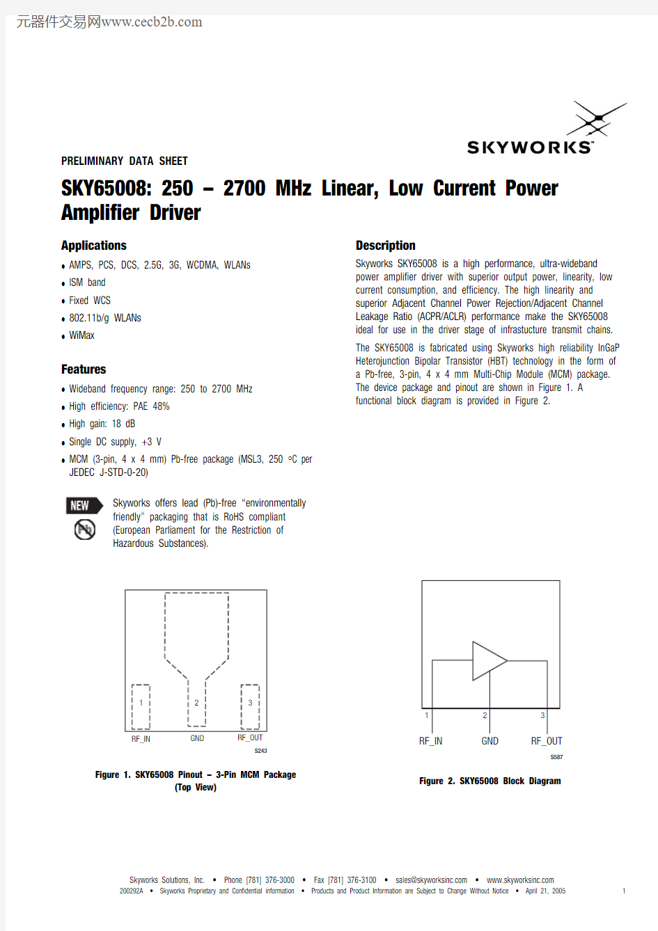
Figure 1. SKY65008 Pinout – 3-Pin MCM Package
(Top View)
Description
Skyworks SKY65008 is a high performance, ultra-wideband
power amplifier driver with superior output power, linearity, low
current consumption, and efficiency. The high linearity and
superior Adjacent Channel Power Rejection/Adjacent Channel
Leakage Ratio (ACPR/ACLR) performance make the SKY65008
ideal for use in the driver stage of infrastucture transmit chains.
The SKY65008 is fabricated using Skyworks high reliability InGaP
Heterojunction Bipolar Transistor (HBT) technology in the form of
a Pb-free, 3-pin, 4 x 4 mm Multi-Chip Module (MCM) package.
The device package and pinout are shown in Figure 1. A
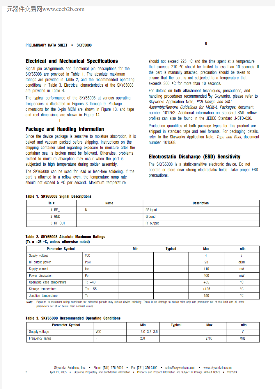
functional block diagram is provided in Figure 2.
2
13
RF_IN GND RF_OUT
S587
Figure 2. SKY65008 Block Diagram
PRELIMINARY DATA SHEET ? SKY65008
Electrical and Mechanical Specifications
Signal pin assignments and functional pin descriptions for the SKY65008 are provided in Table 1. The absolute maximum
ratings are provided in Table 2, and the recommended operating conditions in Table 3. Electrical characteristics of the SKY65008 are provided in Table 4.
The typical performance of the SKY65008 at various operating frequencies is illustrated in Figures 3 through 9. Package
dimensions for the 3-pin MCM are shown in Figure 13, and tape and reel dimensions are shown in Figure 14.
Package and Handling Information
Since the device package is sensitive to moisture absorption, it is baked and vacuum packed before shipping. Instructions on the shipping container label regarding exposure to moisture after the container seal is broken must be followed. Otherwise, problems related to moisture absorption may occur when the part is subjected to high temperature during solder assembly. The SKY65008 can be used for lead or lead-free soldering. If the part is attached in a reflow oven, the temperature ramp rate should not exceed 5 °C per second. Maximum temperature should not exceed 225 °C and the time spent at a temperature that exceeds 210 °C should be limited to less than 10 seconds. If the part is manually attached, precaution should be taken to ensure that the part is not subjected to a temperature that exceeds 300 °C for more than 10 seconds.
For details on both attachment techniques, precautions, and
handling procedures recommended by Skyworks, please refer to Skyworks Application Note, PCB Design and SMT
Assembly/Rework Guidelines for MCM-L Packages , document number 101752. Additional information on standard SMT reflow profiles can also be found in the JEDEC Standard J-STD-020. Production quantities of both package types for this product are shipped in standard tape and reel formats. For packaging details, refer to the Skyworks Application Note, Tape and Reel , document number 101568.
Electrostatic Discharge (ESD) Sensitivity
The SKY65008 is a static-sensitive electronic device. Do not operate or store near strong electrostatic fields. Take proper ESD precautions.
Table 1. SKY65008 Signal Descriptions
Pin #
Name
Description
1 RF_I
N RF input 2 GND Ground 3 RF_OUT
RF output
Table 2. SKY65008 Absolute Maximum Ratings
(T A = +25 °C, unless otherwise noted)
Parameter Symbol Min Typical Max U
nits
Supply voltage VCC
4
V
RF output power P OUT 23 dBm
Supply current I CC 110 mA
Power dissipation P D 400 mW
Operating case temperature T C –40 +85 °C
Storage temperature T ST –55 +125 °C
Junction temperature
T J 150 °C
Note : Exposure to maximum rating conditions for extended periods may reduce device reliability. There is no damage to device with only one parameter set at the limit and all other
parameters set at or below their nominal values.
Table 3. SKY65008 Recommended Operating Conditions
Parameter Symbol Min Typical Max U
nits
Supply voltage VCC 3.0 3.3 3.6 V Frequency range
F
250
2700
MHz
PRELIMINARY DATA SHEET ? SKY65008 Table 4. SKY65008 Electrical Characteristics
(VCC = 3.3 V, T C = 25 °C, input and output load < –8 dB, unless otherwise noted)
Parameter Symbol
Test
Conditions Min Typical Max
U nits
Test Frequency = 900 MHz
Small signal gain G CW 28.5 dB
Output power @ 1 dB compression P1D B CW 19.5 dBm Output 3rd Order Intercept Point OIP3 Two tones, each @
+14 dBm/output tone
34 dBm Noise
figure NF 3.3 dB Test Frequency = 1960 MHz
Small signal gain G CW 20 dB
Output power @ 1 dB compression P1D B CW 21 dBm Output 3rd Order Intercept Point OIP3 Two tones, each @
+5 dBm/output tone
33 dBm Noise
Figure NF 3.0 dB Power-added efficiency PAE CW, P OUT = +20 dBm 42 %
Quiescent current I Q No RF input 76 mA
Output power @ ACPR = –45 dBc P OUT IS-95. Nine forward
channels
14 dBm Test Frequency = 2140 MHz
Small signal gain G CW 20 dB
Output power @ 1 dB compression P1D B CW 21 dBm Output 3rd Order Intercept Point OIP3 Two tones, each @
+5 dBm/output tone
32 dBm Noise
Figure NF 3.0 dB Output power @ ACLR = –45 dBc P OUT 3G-WCDMA.
Downlink
test model #1 with
64 DPCH
11 dBm
Test Frequency = 2450 MHz
Small signal gain G CW 18.5 dB
Output power @ 1 dB compression P1D B CW 20 dBm Output 3rd Order Intercept Point OIP3 Two tones, each @
+5 dBm/output tone
33 dBm Noise
Figure NF 3.0 dB Test Frequency = 2650 MHz
Small signal gain G CW 18 dB
Output power @ 1 dB compression P1D B CW 19 dBm Output 3rd Order Intercept Point OIP3 Two tones, each @
+5 dBm/output tone
32 dBm Noise
Figure NF 3.0 dB
PRELIMINARY DATA SHEET ? SKY65008
850
323130
2928272625870890910930950
Frequency (MHz)
G a i n (d B
)
Figure 3. Typical Small Signal Gain vs Frequency in the 900 MHz Band
1700
21
20
19
181800
1900
2000
2100
2200
Frequency (MHz)
G a i n (d B
)
Figure 4. Typical Small Signal Gain vs Frequency in the 1900 MHz Band
2120
1918172000
205021002150220022502300
Frequency (MHz)
G a i n (d B
)
Figure 5. Typical Small Signal Gain vs Frequency in the 2100 MHz Band
PRELIMINARY DATA SHEET ? SKY65008
2
34.0
33.5
33.0
32.5
32.0
3
4
5
6
7
8
9
10
P OUT (dBm)
O I P 3 (d B )
Figure 6. Typical OIP3 vs Tone Output Power in the 1960 MHz Band
5
–40–45–50
–55–60–65–70–75
6
7
8
9
10
11
12
13
14
15
P OUT (dBm)
A C P R (d
B c
)
Figure 7. Typical ACPR vs Output Power in the 1960 MHz Band
PRELIMINARY DATA SHEET ? SKY65008
+100–10
–20–30–40–50–60–702.41
2.42 2.43 2.44 2.45 2.46 2.47 2.48 2.49
Frequency (GHz)
P o w e r (d B c
)
Figure 8. Spectral Mask Performance @ 2450 MHz (802.11b CCK @ 11 Mbps Input Signal, P OUT = 19 dBm)
+100–10
–20–30–40–50–60
2.40
2.42
2.44
2.46
2.48
2.50
Frequency (GHz)
P o w e r (d B c
)
Figure 9. Spectral Mask Performance @ 2450 MHz (802.11g 64QAM @ 54 Mbps Input Signal, P OUT = 17 dBm)
PRELIMINARY DATA SHEET ? SKY65008
Evaluation Board Description
The Skyworks SKY65008 Evaluation Board is used to test the performance of the SKY65008 power amplifier driver. An
assembly drawing for the Evaluation Board is shown in Figure 10 and the layer detail is provided in Figure 11. Circuit Design Configurations
The following design considerations are general in nature and must be followed regardless of final use or configuration. 1. Paths to ground should be made as short as possible. 2. The ground pad of the SKY65008 power amplifier has special electrical and thermal grounding requirements. This pad is the main thermal conduit for heat dissipation. Since the circuit board acts as the heat sink, it must shunt as much heat as possible from the amplifier. As such, design the connection to the ground pad to dissipate the maximum wattage produced to the circuit board. Multiple vias to the grounding layer are required. NOTE : Junction temperature (T J ) of the device increases with a
poor connection to the slug and ground. This reduces the lifetime of the device.
A suggested matching circuit is shown in Figure 12 with component values listed in Table 5. Testing Procedure
Use the following procedure to set up the SKY65008 Evaluation Board for testing:
1. Connect a 3.3 V supply to VCC. If available, enable the current limiting function of the power supply to 240 mA.
2. Connect a signal generator to the RF signal input port. Set it to the desired RF frequency at a power level of –15 dBm or less to the Evaluation Board but do NOT enable the RF signal.
3. Connect a spectrum analyzer to the RF signal output port.
4. Enable the power supply.
5. Enable the RF signal.
6. Take measurements.
CAUTION : If any of the output signals exceed the rated
maximum values, the SKY65008 Evaluation Board can be permanently damaged.
J1 (RF In)JP1
J2 (RF Out)
S446
Figure 10. Evaluation Board Assembly Drawing
PRELIMINARY DATA SHEET ? SKY65008
Layer 3: Ground
Layer 4: Solid Ground Plane
Layer 1: Top - Metal
S447
Layer 2: Ground
Figure 11. Evaluation Board Layer Detail
PRELIMINARY DATA SHEET ? SKY65008
Output
Input
S586
Figure 12. SKY65008 Evaluation Board Schematic
(Refer to Table 5 for Component Values)
Table 5. SKY65008 Evaluation Board Component Values vs Frequency
Evaluation Board Frequency (MHz)
Component
900 1960 2140 2450 2650
? 0
?
? 0
? 0
? 0
R1 0
? 750
?
? 750
? 750
R2 750
? 750
? 680
? 680
?R3 680
? 680
? 680
μF 1.0
μF
μF 1.0
μF 1.0
μF 1.0
C1 1.0
C2 10 pF 36 pF 6.8 pF 6.8 pF 6.8 pF
C3 18 pF 6.8 pF 36 pF 18 pF 18 pF
L1 47 nH 27 nH 27 nH 18 nH 18 nH
L2 47 nH 27 nH 27 nH 18 nH 18 nH
M1 4.7 nH 1 pF 1 pF 0.5 pF 0.5 pF
M2 5.6 pF 3.9 pF 1.8 pF 1.2 pF 1.0 pF
pF DNC DNC DNC DNC M3 7.5
M4 1.0
pF DNC DNC DNC DNC M5 18 pF 6.8 pF 15 pF 12 pF 12 pF
M6 5.6 nH DNC 1 pF 1 pF 1 pF
PRELIMINARY DATA SHEET ? SKY65008
S506
All measurements are in millimeters
Bottom View
Side View
Figure 13. SKY65008 Package Dimensions
S583
4.35 ± 0.10
Notes:
or 2. Cover tape material: transparent conductive PSA 3. Cover tape size: 9.3 mm width
4. All measurements are in millimeters
A
Figure 14. SKY65008 Tape and Reel Dimensions
PRELIMINARY DATA SHEET ? SKY65008
Ordering Information
Model Name Ordering Part Number Evaluation Kit Part Number
SKY65008 250-2700 MHz Linear, Low Current PA Driver SKY65008-21 TW13-D781-001 (836 MHz)
TW13-D782-001 (900 MHz)
TW13-D783-001 (1960 MHz)
TW13-D784-001 (2140 MHz)
TW13-D786-001 (2450 MHz)
TW13-D787-001 (2650 MHz)
Copyright ? 2005 Skyworks Solutions, Inc. All Rights Reserved.
Information in this document is provided in connection with Skyworks Solutions, Inc. (“Skyworks”) products. These materials are provided by Skyworks as a service to its customers and may be used for informational purposes only by the customer. Skyworks assumes no responsibility for errors or omissions in these materials. Skyworks may make changes to its documentation, products, specifications and product descriptions at any time, without notice. Skyworks makes no commitment to update the information and shall have no responsibility whatsoever for conflicts, incompatibilities, or other difficulties arising from future changes to its documentation, products, specifications and product descriptions.
No license, express or implied, by estoppel or otherwise, to any intellectual property rights is granted by or under this document. Except as may be provided in Skyworks Terms and Conditions of Sale for such products, Skyworks assumes no liability whatsoever in association with its documentation, products, specifications and product descriptions.
THESE MATERIALS ARE PROVIDED “AS IS” WITHOUT WARRANTY OF ANY KIND, EITHER EXPRESS OR IMPLIED OR OTHERWISE, RELATING TO SALE AND/OR USE OF SKYWORKS PRODUCTS INCLUDING WARRANTIES RELATING TO FITNESS FOR A PARTICULAR PURPOSE, MERCHANTABILITY, PERFORMANCE, QUALITY OR NON-INFRINGEMENT OF ANY PATENT, COPYRIGHT OR OTHER INTELLECTUAL PROPERTY RIGHT. SKYWORKS FURTHER DOES NOT WARRANT THE ACCURACY OR COMPLETENESS OF THE INFORMATION, TEXT, GRAPHICS OR OTHER ITEMS CONTAINED WITHIN THESE MATERIALS. SKYWORKS SHALL NOT BE LIABLE FOR ANY DAMAGES, INCLUDING SPECIAL, INDIRECT, INCIDENTAL, OR CONSEQUENTIAL DAMAGES, INCLUDING WITHOUT LIMITATION, LOST REVENUES OR LOST PROFITS THAT MAY RESULT FROM THE USE OF THESE MATERIALS WHETHER OR NOT THE RECIPIENT OF MATERIALS HAS BEEN ADVISED OF THE POSSIBILITY OF SUCH DAMAGE.
Skyworks products are not intended for use in medical, lifesaving or life-sustaining applications. Skyworks customers using or selling Skyworks products for use in such applications do so at their own risk and agree to fully indemnify Skyworks for any damages resulting from such improper use or sale.
The following are trademarks of Skyworks Solutions, Inc.: Skyworks?, the Skyworks logo, and Breakthrough Simplicity?. Product names or services listed in this publication are for identification purposes only, and may be trademarks of Skyworks or other third parties. Third-party brands and names are the property of their respective owners. Additional information, posted at
https://www.doczj.com/doc/ff10620956.html,, is incorporated by reference.