General Description
The MAX6100–MAX6107 are low-cost, low-dropout (LDO), micropower voltage references. These three-ter-minal references are available with output voltage options of 1.25V, 1.8V, 2.048V, 2.5V, 3V, 4.096V, 4.5V, and 5V.They feature a proprietary curvature-correction circuit and laser-trimmed, thin-film resistors that result in a low temperature coefficient of 75ppm/°C (max) and an initial accuracy of ±0.4% (max). These devices are specified over the extended temperature range (-40°C to +85°C).These series-mode voltage references draw only 90μA of supply current and can source 5mA and sink 2mA of load current. Unlike conventional shunt-mode (two-terminal)references that waste supply current and require an external resistor, these devices offer a supply current that is virtually independent of the supply voltage (with only a 4μA/V variation with supply voltage) and do not require an external resistor. Additionally, these internally compen-sated devices do not require an external compensation capacitor and are stable with load capacitance.Eliminating the external compensation capacitor saves valuable board area in space-critical applications. Low-dropout voltage and supply independent, ultra-low sup-ply current make these devices ideal for battery-operat-ed, high-performance, low-voltage systems.
The MAX6100–MAX6107 are available in tiny 3-pin SOT23 packages.
Applications
Portable Battery-Powered Systems Notebook Computers PDAs, GPSs, DMMs Cellular Phones Hard-Disk Drives
Features
o Ultra-Small 3-Pin SOT23 Package o Low Cost
o No Output Capacitor Required o Stable with Capacitive Loads
o Load Regulation (2mA Sink): 8mV/mA (max)
Load Regulation (5mA Source): 0.9mV/mA (max)o ±0.4% (max) Initial Accuracy
o Low 75ppm/°C Temperature Coefficient o 125μA (max) Quiescent Supply Current o 50mV Dropout at 1mA Load Current
MAX6100–MAX6107
Low-Cost, Micropower, Low-Dropout,
High-Output-Current, SOT23 Voltage References
________________________________________________________________Maxim Integrated Products 1
19-1613; Rev 3; 3/02
Ordering Information
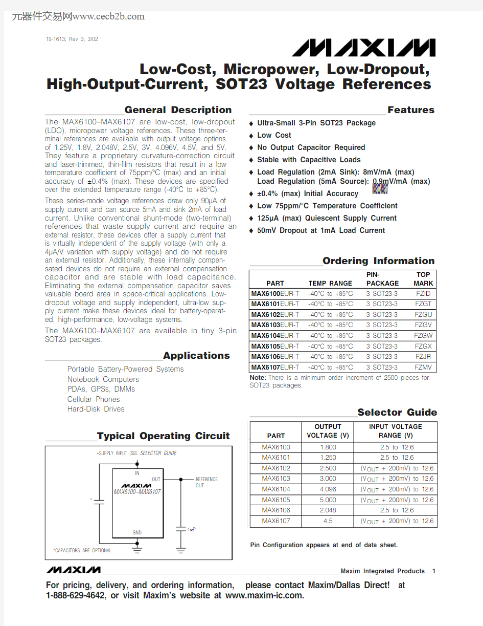
Typical Operating Circuit
For pricing, delivery, and ordering information,please contact Maxim/Dallas Direct!at 1-888-629-4642, or visit Maxim’s website at https://www.doczj.com/doc/f53706610.html,.
Pin Configuration appears at end of data sheet.
M A X 6100–M A X 6107
Low-Cost, Micropower, Low-Dropout,
High-Output-Current, SOT23 Voltage References 2_______________________________________________________________________________________
ABSOLUTE MAXIMUM RATINGS
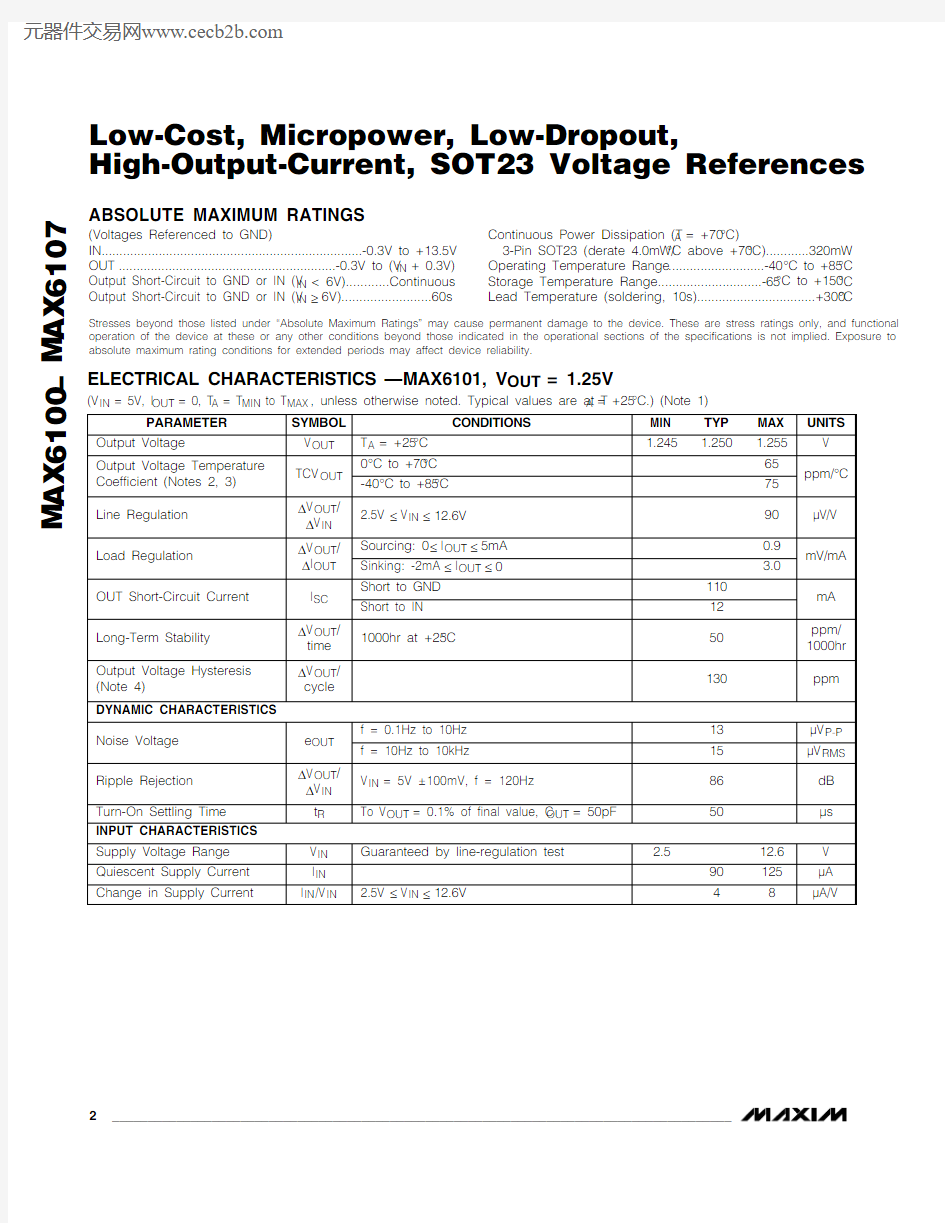
ELECTRICAL CHARACTERISTICS —MAX6101, V OUT = 1.25V
(V IN = 5V, I OUT = 0, T A = T MIN to T MAX , unless otherwise noted. Typical values are at T A = +25°C.) (Note 1)
Stresses beyond those listed under “Absolute Maximum Ratings” may cause permanent damage to the device. These are stress ratings only, and functional operation of the device at these or any other conditions beyond those indicated in the operational sections of the specifications is not implied. Exposure to absolute maximum rating conditions for extended periods may affect device reliability.
(Voltages Referenced to GND)
IN.........................................................................-0.3V to +13.5V OUT .............................................................-0.3V to (V IN + 0.3V)Output Short-Circuit to GND or IN (V IN < 6V)............Continuous Output Short-Circuit to GND or IN (V IN ≥6V).........................60s
Continuous Power Dissipation (T A = +70°C)
3-Pin SOT23 (derate 4.0mW/°C above +70°C)............320mW Operating Temperature Range ...........................-40°C to +85°C Storage Temperature Range.............................-65°C to +150°C Lead Temperature (soldering, 10s).................................+300°C
MAX6100–MAX6107
Low-Cost, Micropower, Low-Dropout,
High-Output-Current, SOT23 Voltage References
_______________________________________________________________________________________3
ELECTRICAL CHARACTERISTICS —MAX6100, V OUT = 1.8V
M A X 6100–M A X 6107
Low-Cost, Micropower, Low-Dropout,
High-Output-Current, SOT23 Voltage References 4_______________________________________________________________________________________
MAX6100–MAX6107
Low-Cost, Micropower, Low-Dropout,
High-Output-Current, SOT23 Voltage References
_______________________________________________________________________________________5
ELECTRICAL CHARACTERISTICS —MAX6102, V OUT = 2.50V
(V IN = 5V, I OUT = 0, T A = T MIN to T MAX , unless otherwise noted. Typical values are at T A = +25°C.) (Note 1)
M A X 6100–M A X 6107
Low-Cost, Micropower, Low-Dropout,
High-Output-Current, SOT23 Voltage References 6_______________________________________________________________________________________
ELECTRICAL CHARACTERISTICS —MAX6103, V OUT = 3.0V
(V IN = 5V, I OUT = 0, T A = T MIN to T MAX , unless otherwise noted. Typical values are at T A = +25°C.) (Note 1)
MAX6100–MAX6107
Low-Cost, Micropower, Low-Dropout,
High-Output-Current, SOT23 Voltage References
_______________________________________________________________________________________7
ELECTRICAL CHARACTERISTICS —MAX6104, V OUT = 4.096V
(V IN = 5V, I OUT = 0, T A = T MIN to T MAX , unless otherwise noted. Typical values are at T A = +25°C.) (Note 1)
M A X 6100–M A X 6107
Low-Cost, Micropower, Low-Dropout,
High-Output-Current, SOT23 Voltage References 8_______________________________________________________________________________________
ELECTRICAL CHARACTERISTICS —MAX6107, V OUT = 4.5V
(V IN = 5V, I OUT = 0, T A = T MIN to T MAX , unless otherwise noted. Typical values are at T A = +25°C.) (Note 1)
MAX6100–MAX6107
Low-Cost, Micropower, Low-Dropout,
High-Output-Current, SOT23 Voltage References
_______________________________________________________________________________________9
Note 1:Devices are 100% production tested at T A = +25°C and are guaranteed by design from T A = T MIN to T MAX by correlation to
sample units characterized over temperature.
Note 2:Temperature coefficient is specified by the “box ” method, i.e., the maximum ?V OUT is divided by the maximum ?t.Note 3:Not production tested. Guaranteed by design.
Note 4:Thermal hysteresis is defined as the change in +25°C output voltage before and after temperature cycling of the device
from T A = T MIN to T MAX .
Note 5:Dropout voltage is the minimum input voltage at which V OUT changes ≤0.2% from V OUT at V IN = 5.0V (V IN = 5.5V for
MAX6105).
ELECTRICAL CHARACTERISTICS —MAX6105, V OUT = 5.000V
(V IN = 5.5V, I OUT = 0, T A = T MIN to T MAX , unless otherwise noted. Typical values are at T A = +25°C.) (Note 1)
M A X 6100–M A X 6107
Low-Cost, Micropower, Low-Dropout,
High-Output-Current, SOT23 Voltage References 10______________________________________________________________________________________
(T A = +25°C, unless otherwise noted.)
2.488
2.4912.4902.4892.4932.4922.4972.4962.4952.494-40
-20
20
40
60
80
MAX6102
OUTPUT VOLTAGE TEMPERATURE DRIFT
TEMPERATURE (°C)
O U T P U T V O L T A G E (V )
4.990
4.9964.9944.992
5.0004.9985.0045.002-40
-20
20
40
60
80
MAX6105
OUTPUT VOLTAGE TEMPERATURE DRIFT
TEMPERATURE (°C)
O U T P U T V O L T A G E (V )0402080601001202
8
10
4
6
12
14
SUPPLY CURRENT vs. INPUT VOLTAGE
M A X 6100/07 T O C 03
INPUT VOLTAGE (V)
S U P P L Y C U R R E N T (μA )
050
150
100
200
250
1
2
3
4
5
MAX6102
DROPOUT VOLTAGE vs. SOURCE CURRENT
SOURCE CURRENT (mA)
D R O P O U T V O L T A G
E (m V )
-90
-70-30-50-10-80
-40-60-200
0.5
1.0
1.5
2.0
2.5
MAX6102
DROPOUT VOLTAGE vs. SINK CURRENT
SINK CURRENT (mA)
D R O P O U T V O L T A G
E (m V )
050
150
100
200
250
2
1
3
4
5
6
MAX6105
DROPOUT VOLTAGE vs. SOURCE CURRENT
SOURCE CURRENT (mA)
D R O P O U T V O L T A G
E (m V )
-90
-70-30-50-10
-80
-40-60-2000
0.5
1.0
1.5
2.0
2.5
MAX6105
DROPOUT VOLTAGE vs. SINK CURRENT
SINK CURRENT (mA)
D R O P O U T V O L T A G
E (m V )
-2
0-121435768
-6
-2
2
-4
4
6
8
10
12
MAX6102 LOAD REGULATION
LOAD CURRENT (mA)
O U T P U T V O L T A G E C H A N G E (m V )
Typical Operating Characteristics (continued)
(T A = +25°C, unless otherwise noted.)
MAX6100–MAX6107
Low-Cost, Micropower, Low-Dropout,
High-Output-Current, SOT23 Voltage References
______________________________________________________________________________________11
-1021435-6
-2
2
-4
4
6
8
1012MAX6105 LOAD REGULATION
LOAD CURRENT (mA)O U T P U T V O L T A G E C H A N G E (m V )
-0.10
0-0.050.100.050.200.150.25268410
12
14
MAX6102 LINE REGULATION
INPUT VOLTAGE (V)O U T P U T V O L T A G E C H A N G E (m V
)-0.05
0.1500.250.200.350.300.40
4
6
8
10
12
14
MAX6105 LINE REGULATION
INPUT VOLTAGE (V)
O U T P U T V O L T A G E C H A N G E (m V )0.050.10100908070605040302000.001
1
10
100
0.01
0.1
1000
MAX6102
POWER-SUPPLY REJECTION RATIO
vs. FREQUENCY
10M A X 6100/07 T O C 13
FREQUENCY (kHz)
P S R R (d B )80
70605040302000.001
1101000.010.11000MAX6105
POWER-SUPPLY REJECTION RATIO
vs. FREQUENCY
10
M A X 6100/07 T O C 14
FREQUENCY (kHz)
P S R R (d B )MAX6101
LINE-TRANSIENT RESPONSE
M A X 6100/07 T O C 15
100μs/div
V IN
200mV/div
V OUT 200mV/div
MAX6102
LINE-TRANSIENT RESPONSE
M A X 6100/07 T O C 16
100μs/div V IN
200mV/div V OUT 100mV/div MAX6105
LINE-TRANSIENT RESPONSE
M A X 6100/07 T O C 17
100μs/div
V IN
200mV/div
V OUT 5mV/div
0.0110010k 10.1101k 100k 1M
OUTPUT IMPEDANCE vs. FREQUENCY
M A X 6100/07 T O C 18
FREQUENCY (Hz)
O U T P U T I M P E D A N C E (?)
-100
1000300200400600700500800
Typical Operating Characteristics (continued)
(T A = +25°C, unless otherwise noted.)
M A X 6100–M A X 6107
Low-Cost, Micropower, Low-Dropout,
High-Output-Current, SOT23 Voltage References 12______________________________________________________________________________________
MAX6105
LOAD-TRANSIENT RESPONSE (C LOAD = 0)
M A X 6100/07 T O C 21
200μs/div 5mA -2mA
V OUT 200mV/div I OUT 5mA/div
MAX6102
LOAD-TRANSIENT RESPONSE (C LOAD = 1μF)
M A X 6100/07 T O C 22
200μs/div
V IN 2V/div
V OUT 50mV/div
MAX6105
LOAD-TRANSIENT RESPONSE (C LOAD = 1μF)
M A X 6100/07 T O C 23
100μs/div
V IN 5V/div
V OUT 50mV/div
MAX6101
TURN-ON TRANSIENT
M A X 6100/07 T O C 24
100μs/div
V IN 2V/div
V OUT 500mV/div
MAX6101
LOAD-TRANSIENT RESPONSE (C LOAD = 0)
M A X 6100/07 T O C 19
200μs/div
4mA
-2mA
V OUT 200mV/div
I OUT 5mA/div
MAX6102
LOAD-TRANSIENT RESPONSE (C LOAD = 0)
M A X 6100/07 T O C 20
200μs/div
5mA -2mA
V OUT 200mV/div
I OUT 5mA/div
MAX6100–MAX6107
Low-Cost, Micropower, Low-Dropout,
High-Output-Current, SOT23 Voltage References
______________________________________________________________________________________13
Applications Information
Input Bypassing
For the best line-transient performance, decouple the input with a 0.1μF ceramic capacitor as shown in the Typical Operating Circuit . Locate the capacitor as close to IN as possible. Where transient performance is less important, no capacitor is necessary.
Output/Load Capacitance
Devices in the MAX6100 family do not require an output capacitance for frequency stability. They are stable for any capacitive load when sourcing less than 200μA.When sourcing greater than 200μA, the output may become unstable with capacitive loads between 0.5nF and 50nF. In applications where the load or the supply can experience step changes, an output capacitor reduces the amount of overshoot (undershoot) and improves the circuit ’s transient response. Many applica-tions do not require an external capacitor, and the MAX6100 family can offer a significant advantage in these applications when board space is critical.
Supply Current
The quiescent supply current of the series-mode MAX6100 family is typically 90μA and is virtually indepen-dent of the supply voltage, with only an 8μA/V (max) vari-ation with supply voltage. Unlike series references,shunt-mode references operate with a series resistor con-nected to the power supply. The quiescent current of a shunt-mode reference is thus a function of the input volt-age. Additionally, shunt-mode references have to be biased at the maximum-expected load current, even if the load current is not present at the time. I n the MAX6100family, the load current is drawn from the input voltage only when required, so supply current is not wasted and efficiency is maximized at all input voltages. This improved efficiency reduces power dissipation and extends battery life. When the supply voltage is below the minimum specified input voltage (as during turn-on), the devices can draw up to 400μA beyond the nominal supply current. The input voltage source must be capable of providing this current to ensure reliable turn-on.
Output Voltage Hysteresis
Output voltage hysteresis is the change of output voltage at T A = +25°C before and after the device is cycled over its entire operating temperature range. Hysteresis is caused by differential package stress appearing across the bandgap core transistors. The typical tem-perature hysteresis value is 130ppm.
Typical Operating Characteristics (continued)
(T A = +25°C, unless otherwise noted.)
MAX6105
TURN-ON TRANSIENT
M A X 6100/07 T O C 25
100μs/div
V IN 2V/div
V OUT 2V/div
MAX6102
0.1Hz TO 10Hz OUTPUT NOISE
M A X 6100/07 T O C 26
1s/div 20μV/div MAX6105
0.1Hz TO 10Hz OUTPUT NOISE
M A X 6100/07 T O C 27
1s/div
20μV/div
M A X 6100–M A X 6107
Low-Cost, Micropower, Low-Dropout,
High-Output-Current, SOT23 Voltage References Maxim cannot assume responsibility for use of any circuitry other than circuitry entirely embodied in a Maxim product. No circuit patent licenses are implied. Maxim reserves the right to change the circuitry and specifications without notice at any time.
14____________________Maxim Integrated Products, 120 San Gabriel Drive, Sunnyvale, CA 94086 408-737-7600?2002 Maxim Integrated Products
Printed USA
is a registered trademark of Maxim Integrated Products.
Turn-On Time
These devices typically turn on and settle to within 0.1%of their final value in 50μs to 300μs. The turn-on time can increase up to 1.5ms with the device operating at the minimum dropout voltage and the maximum load.
Chip Information
TRANSISTOR COUNT: 117
Package Information
(The package drawing(s) in this data sheet may not reflect the most current specifications. For the latest package outline information,go to https://www.doczj.com/doc/f53706610.html,/packages .)