Electric-field induced dipole blockade with Rydberg atoms
- 格式:pdf
- 大小:205.99 KB
- 文档页数:4

拉比振荡
拉比振荡简介
激光脉冲打入物质中,引起介质上下能级粒子数周期性反转。
振荡频率称为为拉比频率,此过程发生的前提条件是脉冲时间小于介质的驰豫时间,且不考虑阻尼。
这样可以理解为粒子处于的激发态寿命大于脉冲的作用时间。
拉比振荡
历史背景
[1]1987年,实验发现了称为拉比(Rabi)振荡的效应。
在实验中,向不完全真空、且有一定热辐射(2.5K)的腔体内,注入高激发态的里德堡原子,由于所发出的光子在腔体内停留的时间长,高激发态原子在跃迁时,偶极矩又较大,使原子在腔内的自发辐射有可能是可逆的,即反复地释放和吸收光子,这就使原子在上下两能级间来回振荡。
当原子跃迁频率恰与某一腔频共振时,即可观察到拉比振荡现象。
模型特点
[2]一个处于拉比振荡的粒子处在能量基态被激发到激发态的概率C成sin平方分布,此外,当所加光场的频率远离两能级的共振线时,将失去场对原子的的作用。
荆轲,一个四处为家的刺客,他的心犹如浮云,心如飘蓬,是没有根的,然而高渐离的筑声,却成了他愿意停留在燕国这片土地上的原由。
虽是初见,却如故人。
也许所有的遇见,早已经是前世的注定,没有早晚,刚好在合适的时间遇见你,就是最美的相识。
他曾经游历过多少地方,自己已经数不清,但是没有一处可以挽留他行走的脚步,唯有今日高渐离的筑声,让他怎么也舍不得离开。

量子阱中rashba自旋—轨道耦合的rabi劈裂效应嘿,朋友!你知道量子阱中 rashba 自旋—轨道耦合的 rabi 劈裂效应吗?这玩意儿听起来是不是特别高深莫测,仿佛是来自遥远宇宙深处的神秘密码?咱先来说说这量子阱。
你就把它想象成一个特别神奇的小“坑”,里面的粒子就像调皮的小精灵,到处蹦跶。
而这个 rashba 自旋—轨道耦合呢,就像是小精灵们玩耍时的一种特殊规则。
想象一下,咱们平常玩游戏都有规则吧?比如跳皮筋得按特定的节奏跳,踢毽子不能用手碰。
这 rashba 自旋—轨道耦合也是类似的,它决定了粒子们在量子阱这个小“坑”里怎么运动,怎么相互作用。
那 rabi 劈裂效应又是啥呢?这就好比一场热闹的音乐会。
本来乐队演奏得好好的,声音很和谐。
可突然来了个特别的因素,就像有人在乐队里敲了一记特别响的鼓,整个音乐的节奏和声音就发生了变化。
rabi 劈裂效应就是这个突然出现的“特别响的鼓”,让量子阱里粒子的状态发生了显著的改变。
你说神奇不神奇?这量子阱里的世界,可比咱们肉眼看到的世界复杂多了,也有趣多了。
咱再深入聊聊这个 rabi 劈裂效应。
它可不是随随便便就出现的,得有特定的条件。
就像植物生长需要阳光、水分和土壤一样,rabi 劈裂效应的出现也得有合适的环境。
比如说,粒子的能量得达到一定的值,或者外部施加的电磁场强度得恰到好处。
你可能会问,研究这个有啥用呢?这用处可大了去啦!就好比咱们发明了指南针,能在茫茫大海中找到方向。
了解量子阱中 rashba 自旋—轨道耦合的rabi 劈裂效应,能让咱们在微观世界里找到新的“方向”,说不定就能开发出超级厉害的新技术呢!比如说更高效的电子设备,或者更精准的量子计算。
想想看,未来的电脑可能快得像闪电,手机的功能强大到超乎想象,这一切都可能源于对这个看似神秘的效应的研究。
所以啊,别小看这量子阱中 rashba 自旋—轨道耦合的 rabi 劈裂效应,它说不定就是打开未来科技大门的一把神奇钥匙呢!。

学号:201105774题目名称: 强耦合下的光子阻塞效应研究题目类型: 研究论文学生姓名: 董昌瑞院(系): 物理与光电工程学院专业班级: 物理11102班指导教师: 邹金花辅导教师: 邹金花时间: 2015年1月至2015年6月目录毕业论文任务书` (I)指导教师评审意见 (VIII)评阅教师评语 (IX)答辩记录及成绩评定 (X)中文摘要 (XI)外文摘要 (XII)1引言 (1)2 基础理论知识 (1)2.1 光力振子系统 (1)2.2二能级原子与光场相互作用的全量子理论 (2)2.3光场关联函数 (5)2.4 光子计数统计 (8)3 模型方程与结果分析 (10)3.1模型方程 (10)3.2 方程分析 (12)4总结与展望 (14)参考文献 (14)致谢 (16)毕业论文任务书`院(系)物理与光电工程学院专业物理班级物理11102 学生姓名董昌瑞指导教师/职称邹金花/副教授1.毕业论文(设计)题目:强耦合下的光子阻塞效应研究2.毕业论文(设计)起止时间: 2015 年1月1 日~2015 年 6月10 日3.毕业论文(设计)所需资料及原始数据(指导教师选定部分)[1] A Ridolfo, M Leib, S Savasta, M J Hartmann. Photon Blockade in the Ultrastrong CouplingRegime [J]. Phys. Rev. Lett., 2012, 109: 193602-1~193602-5[2] Jieqiao Liao, C K Law. Cooling of a mirror in cavity optomechanics with a chirped pulse [J]. Phys. Rev. A, 2011, 84: 053838-1~053838-6[3] P Komar, S D Bennett, K Stannigel, S J M Habraken, P Rabl, P Zoller, M D Lukin. Single-photon nonlinearities in two-mode optomechanics [J]. Phys. Rev. A, 2013, 87: 013839-1~013839-10[4] T Ramos, V Sudhir, K Stannigel, P Zoller, T Kippenbrg. Nonlinear quantum optomechanics viaindividual intrinsic two-level defects [J]. Phys. Rev. Lett., 2013, 110: 193602-1~193602-5 [5] G Anetsberger, O Arcizet, Q P Unterreithmeier, R Riviere, A Schliesser, E M Weig, J P Kotthaus,T Kippenberg. Near-field cavity optomechanics with nanomechanical oscillators [J]. Nat. Phys., 2009, 5: 909~914[6] S J M Habraken, W Lechner, P Zoller. Resonances in dissipative optomechanics withnanoparticles: Sorting, speed rectification, and transverse coolings [J]. Phys. Rev. A, 2013, 87: 053808-1~053808-8[7] K Qu, G S Agarwal. Fano resonances and their control in optomechanics [J]. Phys. Rev. A, 2013,87: 063813-1~063813-7[8] A Nunnenkamp, K Borkje, S M Girvin. Cooling in the single-photon strong-coupling regime ofcavity optomechanics [J]. Phys. Rev. A, 2012, 85: 051803-1~051803-4[9] Y C Liu, Y F Xiao, X S Luan, C W Wong. Dynamic Dissipative Cooling of a MechanicalResonator in Strong Coupling Optomechanics [J]. Phys. Rev. A, 2013, 110: 153606-1~153606-5[10] A Nunnekamp, K Borkie, S M Girvin. Single-photon optomechanics [J]. Phys. Rev. Lett., 2011,107: 063602-1~063602-5[11] J M Dobrindt, I Wilson-Rae, T J Kippenbeg. Parametric Normal-Mode Splitting in CavityOptomechanics [J]. Phys. Rev. Lett., 2008, 101: 263602-1~263602-4[12]樊菲菲. 光力振子与原子间量子纠缠和振子压缩的研究[D]. 华中师范大学,2014[13] 张文慧. 光机械腔系统的动力学行为[D]. 华中师范大学,2014[14]詹孝贵. 腔光机械系统中电磁诱导透明及其相关现象的理论研究[D]. 华中科技大学,20134.毕业论文(设计)应完成的主要内容在阅读大量文献的基础上,完成开题报告,并通过开题答辩。

3国家863激光技术领域资助课题。
1996年9月17日收到原稿,1997年10月27日收到修改稿。
李家胤,男,1944年12月出生,教授。
相对论磁控管的实验研究李家胤 熊祥正 杨梓强 周晓岚 胡绍湘张 冰 马文多 李 慎 李明光 梁 正 刘盛纲 (电子科技大学高能所,强辐射重点实验室 610054) 摘要 简要分析了相3对论磁控管的主要特点与问题,编制了谐振系统数值计算程序,通过数值计算与冷测,对不同阴极尺寸与输出结构的磁控管进行了研究,清晰地描述了磁控管的振荡模式与简并现象。
制作了A 6型相对论磁控管并进行了热测实验,研究了输出功率与工作磁场的关系,经过大量优化工作,在S 波段获得了380MW 的微波辐射。
关键词 相对论磁控管 数值计算 高功率微波 相对论磁控管是一种重要的高功率微波器件。
由于它结构简单、牢固、工作可靠性高,具有高功率与重复脉冲工作的潜力,同时也具有多管锁相工作,合成更大功率的可能性,因而受到了以应用为主要目标的科技工作者的高度重视。
美国、俄罗斯、英国和其它国家的科学家们对相对论磁控管进行了长期的研究。
取得了一系列引人注目的成果。
最值得注意的有三个方面:一是实现了重复频率高平均功率工作。
如L 波段相对论磁控管在电压为750kV 、束流为10kA 、脉宽为60n s 的条件下,当重复频率为100H z 时P ^=1.0G W ,P -=4.4k W ,峰值效率达13%,能量效率为9.8%;当重复频率为250H z 时,P ^=600MW ,P -=6.3k W ,峰值效率达8%,能量效率为5.6%。
如此高的平均功率是其它器件尚未达到的。
二是实现了四只和七只相对论磁控管的相位互锁,显示了用多个源产生相干振荡的潜力。
三是实现了宽范围的调频,调频范围达33%,重复频率达100H z ,输出功率达400~600MW ,这些进展有可能使相对论磁控管成为最先获得实际应用的高功率微波源之一。
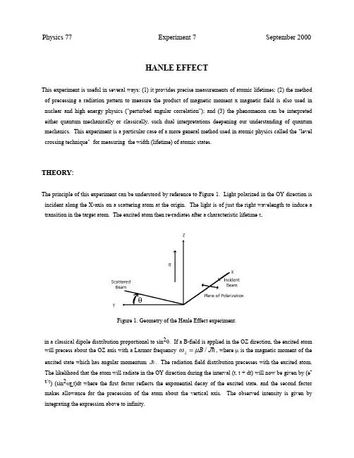
Physics 77 Experiment 7 September 2000HANLE EFFECTThis experiment is useful in several ways: (1) it provides precise measurements of atomic lifetimes; (2) the method of precessing a radiation pattern to measure the product of magnetic moment x magnetic field is also used in nuclear and high energy physics ("perturbed angular correlation"); and (3) the phenomenon can be interpreted either quantum mechanically or classically, such dual interpretations deepening our understanding of quantum mechanics. This experiment is a particular case of a more general method used in atomic physics called the "level crossing technique" for measuring the width (lifetime) of atomic states.THEORY:The principle of this experiment can be understood by reference to Figure 1. Light polarized in the OY direction is incident along the X-axis on a scattering atom at the origin. The light is of just the right wavelength to induce a transition in the target atom. The excited atom then re-radiates after a characteristic lifetime τ,θFigure 1. Geometry of the Hanle Effect experiment.in a classical dipole distribution proportional to sin2θ. If a B-field is applied in the OZ direction, the excited atomwill precess about the OZ axis with a Larmor frequency ωµL B J=/!, where µ is the magnetic moment of the excited state which has angular momentum J!. The radiation field distribution precesses with the excited atom. The likelihood that the atom will radiate in the OY direction during the interval (t, t + dt) will now be given by (e-t/τ) (sin2ωL t)dt where the first factor reflects the exponential decay of the excited state, and the second factor makes allowance for the precession of the atom about the vertical axis. The observed intensity is given by integrating the expression above to infinity.Radiation observed along 0Y;e tdt t L L −∞=+z /sin ()τωτωτ220214(1)A plot of the intensity observed along the OY axis, as a function of B, has its minimum value atB (or ωL ) = 0, with an increase to one-half of its asymptotic value at ωL t = 1/2 or:B g J 1202/=!µτ(2)where µ0 is the Bohr magneton and g J is the electronic g factor for the excited state. The mean life τ can be determined from B l/2 if µ is known (µ=g J µ0J). These measurements always detect the product µτ and one must have additional information to get individual values of τ and µ. We will calculate the value of µ on the assumption that the state is described approximately by ""L S • coupling, in which case:g S S L L J J J =++−++321121()()()(3)See the Optical Pumping writeup (Experiment 8) for the derivation. [The Lurio paper expression for I(τ) isincorrect. The correct expression is discussed by V. Leyva in the Hanle Effect Experiment Reference binder.]Figure 2. Term Diagram for Mercury (Hg).THE EXPERIMENTThe optical system consists of a source arm and an orthogonal detector arm. The source arm contains a low-pressure mercury discharge lamp, a quartz collimating lens, and a UV-transmitting polarizing filter. The absorption/scattering cell is located at the intersection of the optical axes of the two arms. The detector arm contains a second UV-polarizing filter, a quartz lens to focus scattered light onto a detector, an interference bandpass filter centered on 253.7 nm (15.0 nm FWHM), and a UV-sensitive photomultiplier. Polarizing filters that function efficiently at the short UV wavelengths are used (ordinary "Polaroid" filters are totally opaque at UV wavelengths.) in both the lamp and detector arms. The description above of the principle of the experiment leaves out details such as incident line shape, trapping, collision broadening, etc. The reprint by de Zafra describes these complications and the analysis of results. The Franken and Happer papers go further into the theory.Figure 3. Experimental setup for the Hanle Effect experiment.INSTRUMENTATION AND APPARATUSLAMP:The lamp consists of a pair of electrodes sealed into a synthetic quartz capillary that is folded into a hairpin shape. It is filled with natural abundance Hg at a low pressure (~1 atmosphere at operating temperature). An ideal light source would emit a spectrum that exhibits the natural width of the upper radiating 3P1 state. (See the term diagram Figure 2.) However, if there are unexcited Hg atoms in the 1S0 ground state, populating the hollow sheath surrounding the excited cylindrical core of the radiating source, these unexcited atoms will absorb some of the emitted radiation. If the absorbing atoms are cold, and the radiating atoms hot (the usual situation since the temperature will decrease from the centerline to the lamp wall), the spectral line emitted from the hot atoms is wider than the absorption line of the cooler atoms, and what escapes from the source has a dip in the middle. This phenomenon is called self-reversal. We can minimize this problem by running the source as cool as possible (by reducing the operating voltage). That action has the further benefit of reducing Doppler broadening by keeping the internal lamp pressure from rising excessively. Caution: The Hg lamp emits 95% of its energy in the 253.7 nm line. Don't look directly at the bare lamp for extended periods of time without eyeglasses. It also produces copious quantities of O3 (ozone) when operated in open air. It is mounted in a closed housing to completely shield the UV from the user and minimize the production of O3.ABSORPTION/SCATTERING CELL:The absorption cell, constructed from UV transmitting synthetic quartz, is known as a Wood's Horn. It is entirely covered with a black light-absorbing coating except for the entrance and exit windows. The shape, plus coating, insures a minimum of internal reflections so that incident light will encounter the resident Hg atoms only once before reflections alter its plane of polarization. Isotopically pure 198Hg has been used for the absorption/scattering material, unlike the lamp which is filled with natural-abundance Hg (10% 198Hg).DETECTOR:The detector (SSR Quantum Photometer) consists of a UV-sensitive photomultiplier (PMT), a high voltage power supply, and a count-rate meter/nano-ammeter. The operating voltage for the 1P28 PMT has been carefully adjusted to produce the maximum gain at minimum noise (i.e., the optimum signal-to-noise ratio), and is not altered by the user. The count-rate meter mode is used for very low intensities (<108 cps), while the nano-Ammeter (nA) mode (normally used) extends measurement capability to higher intensities. The nA mode allows selection of severalcompromise between low statistical uncertainty and realistic response time. An adjustable zero offset is also available that allows easy examination of a small percentage change in signal strength. The UV interference filter installed at the PMT entrance window passes only the wavelength of interest, substantially improving the signal-to-noise ratio of the system, while insuring that room lighting will neither damage the PMT photocathode nor seriously influence the intensity data.FIELD COMPENSATION COIL SETS 1 & 2:It is necessary to cancel out the ambient magnetic field at the Hg cell. This is accomplished with two pairs of rectangular coils (Sets 1 & 2), in the Helmholtz configuration, driven by two independently adjustable power supplies. Careful positioning of the plane of one pair normal to the horizontal component of the ambient field (rotating the entire experiment on the table), allows the use of only two pairs of coils instead of three. The two power supplies are operated in their Constant Voltage mode, since the current required is too small for sensitive current adjustment or regulation when the supply is in the Constant Current mode..MAGNETOMETER:An air-driven magnetometer is used for the adjustment of the currents through the field-canceling coils. This is a sphere of copper [Oxygen-Free High-Conductivity (OFHC) grade], supported on non-magnetic copper-beryllium ball bearings and rotated about its axis by two jets of air. A central hole has been drilled through the rotor at right angles to the axis of rotation. Two 10,000 turn coils, connected in series-aiding, closely surround the rotor. When the Cu sphere rotates, it is a single turn that cuts any magnetic field lines that may be present. Large eddy currents are induced in the low-resistance single turn which then induce a signal in the fixed coils. It is this signal that is displayed on the Oscilloscope (CRO). The ball bearings are not as hard or durable as ordinary hardened steel (magnetic) ball bearings, which limits the speed of rotation to <600 rps, i.e., a driving air pressure of less than 2-3 psi. The Tektronix 503 CRO is operated in the Differential Input mode to suppress rather large common-mode signals at line frequency and its harmonics.HELMHOLTZ COIL SET 3:A known magnetic field can be applied to the scattering cell by means of a third set of coils (Set 3), a circular pair, also in the Helmholtz configuration. A stable regulated power supply (in Constant-Current mode), a reversing switch, and a digital Ammeter complete this system. The field conversion factor for this pair is 1.87 Gauss/Ampere.DATA ANALYSIS:The laboratory PCs contain useful programs for analyzing the data from this experiment. Math CAD and FFIT are available, and Curvefit (Mathematica) and FFIT are quite capable of fitting a Lorentzian.PRELAB EXERCISE1. Read the de Zafra paper to understand the principles of the experiment.2. Estimate B l/2 for the 3P l state of Hg (τ = ~10-7 sec [See TASK 7.]) for the current geometry. How does this compare to the earth's magnetic field and any stray fields expected in the laboratory?EXPERIMENTAL TASKS:1. Replace the Hg cell with the Vantson magnetometer by rotating the support. A manual describing the magnetometer is available. In essence, it is a generator with output voltage:V peak to peak x B T V S Gauss ().,−−=−⋅286104c h (4)where T is the period of the AC output of the generator. Drive the magnetometer with compressed air at about 2-3psi pressure. Trigger the CRO from the 60 Hz LINE and "tweak" the rotor speed (air pressure) to obtain a stable display at a precise harmonic of 60 Hz. Adjust the currents in the horizontal and vertical bucking coils to minimize the output voltage when the magnetometer axis is oriented properly. The axis of rotation is perpendicular to the disk containing the air inlet and output connector. A small AC field will persist and cannot be canceled with the present arrangement. What is the source of this field? What is the minimum DC field you can produce at the absorption cell? What are the magnitudes of the two components of the ambient DC magnetic field? Record the voltage settings for the two bucking coils and keep them constant for the duration of the experiment.2. Familiarize yourself with the operation of the photometer. A separate manual on the SSR photometer is available.3. Turn on the Hg lamp, beginning with a Variac voltage of 100 V. If the lamp starts to flicker, increase the voltage slightly (1-2 V) until the flicker stops. Wait 15-20 minutes for equilibrium to be reached. The lamp should be run at a voltage that is low enough to produce narrow emission lines without flicker, but high enough (<105 V) to give a good signal-to-noise ratio.4. Adjust the magnetic field produced by the Helmholtz coils (Set #3) to find the minimum and maximum photometer readings. Set the magnetic field such that photometer reads halfway between minimum and maximumvalues and check the peak symmetry when the field is reversed. If asymmetry is more than a few percent, and if the earth's magnetic field has been properly minimized, the polarizer(s) probably needs adjustment. Ask instructor for help.5. Measure and plot the yield of photons scattered at 90° as a function of B (vertical) produced by the Set #3 Helmholtz coils. Repeat the measurements enough to make certain that lamp intensity and scattering cell temperature are not drifting rapidly with time. Even if you have evidence of a slow time dependence, you can make an accurate measure of the half-width of the current dip by measuring the depth of the dip and then setting the current quickly to give a signal at half the full magnitude. Reverse the current to see whether the dip is symmetrical about B vert = 0.6. Repeat step (5) when the tip of the cell is placed in cool water from a refrigerated water cooler. Ice water, or colder baths, will be too cold, reducing the Hg vapor pressure in the absorption cell to a level too low to produce a usable signal.7. Compute the lifetime of the 3P1 state of Hg. Explain the temperature dependence of your results. Compare with the accepted value of τ = 118 ns ±3% (Radzig & Smirnov). Mathematica 3.0, Math CAD and FFIT, on the PC's, are available for fitting Lorentzians.QUESTIONS:(1) How much of your B = 0 signal is due to dark current? How much to room lights? Where does the rest come from?(2) Why do you want the Hg lamp cool?(3) How will self reversal of the 253.7 nm line from the Hg lamp affect the shape of the light curve? How will it affect the determination of the 3P l lifetime?(4) How does the number of Hg vapor (atoms/cm3) vary with temperature? How does this affect the coherent-trapping process? How does this in turn influence the "lifetime" that you observe? Could you remove one of the polarizers and still get good data? Which one is most important? How would you correctly set the UV Polarizers when setting up an experiment for the first time?(5) Why was expensive isotopically pure 198Hg used to fill the scattering cell? How would the data be altered if natural abundance Hg were substituted?(6) Why is the scattering cell shaped, and coated, the way it is? Would satisfactory results be obtained if the simpler right-cylindrical geometry had been used?REFERENCES:1. P. A. Franken, "Interference Effects in the Resonance Fluorescence of "Crossed" Excited Atomic States," Phys. Rev. 121, 508 (1961).2. A. Lurio, R. L. deZafra, and R. J. Goshen, "Lifetime of the First 1P1 State of Zinc, Calcium, and Strontium," Phys. Rev.,A134, 1198 (1964).3. A. C. G. Mitchell and Zemansky, Resonance Radiation and Excited Atoms, (Cambridge University Press, 1971).4. A. A. Radzig & Smirnov, Reference Data on Atoms, Ions, & Molecules, (Springer-Verlag, 1985).5. W. Happer, Review article bound in Reference binder.6. R. L. deZafra and W. Kirk, "Measurement of Atomic Lifetimes by the Hanle Effect," Amer. J. Phys.35, 573 (1967).7. G. Moruzzi and F. Strumia, The Hanle Effect and Level - Crossing Spectroscopy, (Plenum Press, 1991).8. R. Ignace, K. H. Nordsieck, and J. P. Cassinelli, "The Hanle Effect as a Diagnostic of Magnetic Fields in Stellar Envelopes. I. Theoretical Results for Integrated Line Profiles," The Astrophysical Journal, 486, 550 (1997) and II, The Astrophysical Journal, 520, 335 (1999). These two papers are good examples of modern applications of the。

《激子是电子-光子纠缠态》
欧阳森
2016年11月13日
根据目前物理学对激子的定义和实验结果,可以确认激子是电子-光子纠缠
[1]欧阳森《宇宙结构及力的根源》2010年7月第一版中国作家出版社(香港)
[2]欧阳森《白洞喷发与轻元素循环》2011年12月暨南大学出版社
[3]欧阳森《建立宇宙密码字典》2013年11月第一版暨南大学出版社
[4]焦善庆、蓝其开《亚夸克理论》1996年重庆出版社
[5]欧阳森《物理学研究中的陷阱:论现代物理学的错误所在》2015年3月暨南大学出版社
[6]欧阳森《物理学研究中的陷阱:论现代物理学的错误所在》(第二版)2015年12月暨南大学出版社
[7]冯天岳著《斥力在宇宙学中的应用》 1994年1月第一版文津出版社
[8] 冯天岳《斥力定律与后星系宇宙模型》1989年3月《潜科学》杂志
[9]徐宽《物理学的新发展——对爱因斯坦相对论的改正》2005年12月天津科技翻译出版社
[10]李振寰编《元素性质数据手册》1985年7月河北人民出版社。

Chapter 3Breakdown VoltageThe most unique feature of power semiconductor devices is their ability to withstand high voltages. In transistors designed for microprocessors and semiconductor memories, the pressure to reduce their size to integrate more devices on a monolithic chip has resulted in a reduction in their operating voltage. In contrast, the desire to control larger power levels in motor drive and power distribution systems has encouraged the development of power devices with larger breakdown voltages. Typical applications for power devices were illustrated in Fig. 1.2. Depending upon the application, the breakdown voltage of devices can range from 20 to 30 V for voltage regulator modules (power supplies) used to deliver power to microprocessors in personal computers and servers to over 5,000 V for devices used in power transmission networks.In a semiconductor, the ability to support high voltages without the onset of significant current flow is limited by the avalanche breakdown phenomenon, which is dependent on the electric field distribution within the structure. High electric fields can be created within the interior of power devices as well as at their edges. The design optimization of power devices must be performed to meet the breakdown voltage requirements for the application while minimizing the on-state voltage drop, so that the power dissipation is reduced.Power devices are designed to support high voltages within a depletion layer formed across either a P–N junction, a metal–semiconductor (Schottky barrier) contact, or a metal–oxide–semiconductor (MOS) interface. Any electrons or holes – that enter the depletion layer either due to the space-charge generation phenomenon or by diffusion from adjacent quasineutral regions – are swept out by the electric field produced in the region by the applied voltage. As the applied voltage is increased, the electric field in the depletion region increases, resulting in acceleration of the mobile carriers to higher velocities. In the case of silicon, the mobile carriers attain a saturated drift velocity of 1 × 107 cm s−1 when the electric B.J. Baliga, Fundamentals of Power Semiconductor Devices, doi: 10.1007/978-0-387-47314-7_3,© Springer Science + Business Media, LLC 200892 FUNDAMENTALS OF POWER SEMICONDUCTOR DEVICESfield exceeds 1 × 10⁵ V cm −1 as discussed in Chap. 2. With further increase in the electric field, the mobile carriers gain sufficient kinetic energy from the electric field, so that their interaction with the lattice atoms produces the excitation of electrons from the valence band into the conduction band. The generation of electron–hole pairs due to energy acquired from the electric field in the semiconductor is referred to as the impact ionization . Since the electron–hole pairs created by impact ionization also undergo acceleration by the electric field in the depletion region, they participate in the creation of further pairs of electrons and holes. Consequently, impact ionization is a multiplicative phenomenon, which produces a cascade of mobile carriers being transported through the depletion region leading to a signi-ficant current flow through it. Since the device is unable to sustain the application of higher voltages due to a rapid increase in the current, it is considered to undergo avalanche breakdown . Thus, avalanche breakdown limits the maximum operating voltage for power devices. In this chapter, the physics of avalanche breakdown is analyzed in relation to the properties of the semiconductor region that is supporting the voltage. After treating the one-dimensional junction, the edge terminations for power devices are described. Power devices require special edge terminations due to their finite area. The electric field at the edges usually becomes larger than in the middle of the device leading to a reduction of the breakdown voltage. Significant effort has been undertaken to develop a good understanding of the electric field enhancement at the edges, and methods have been proposed to mitigate the increase in the electric field. Various edge termination approaches are discussed in detail in this chapter because of their importance to maximizing the performance of power devices.3.1 Avalanche BreakdownThe maximum voltage that can be supported by a power device before the onset of significant current flow is limited by the avalanche breakdown phenomenon. In power devices, the voltage is supported across depletion regions. As discussed in Chap. 2, mobile carriers are accelerated in the presence of a high electric field until they gain sufficient energy to create hole–electron pairs upon collision with the lattice atoms. This impact ionization process determines the current flowing through the depletion region in the presence of a large electric field. An impact ionization coefficient was defined in Chap. 2 as the number of electron–hole pairs created by a mobile carrier traversing 1 cm through the depletion region along the direction of the electric field. The impact ionization coefficients for electrons and holes are a strong function of the magnitude of the electric field as shown in Fig. 2.10.3.1.1 Power Law Approximations for the Impact Ionization CoefficientsIt is convenient to use a power law, referred to as the Fulop’s approximation 1:357F (Si) 1.810E α−=×(3.1)Breakdown Voltage93for the impact ionization coefficients even though they actually increase exponentially with increasing electric field, when performing analytical derivations pertinent to the performance of silicon power devices. The impact ionization coefficient obtained by using this approximation is shown in Fig. 3.1 by the dashed line together with the impact ionization coefficient for electrons in silicon as governed by the Chynoweth’s law (shown by the solid line). In the same manner, it is convenient to use the Baliga’s power law approximation 2 for the impact ionization coefficients for 4H-SiC for analytical derivations:427B (4H-SiC) 3.910.E α−=×(3.2)The impact ionization coefficient obtained by using this approximation is also shown in Fig. 3.1 by the dashed line together with the impact ionization coefficient for holes in 4H-SiC as governed by the Chynoweth’s law (shown by a solid line).various edge terminations on the breakdown voltage. These analytical solutions the design of improved device structures.provide insight into the physics determining the breakdown phenomenon, enabling94 FUNDAMENTALS OF POWER SEMICONDUCTOR DEVICES3.1.2 Multiplication CoefficientThe avalanche breakdown condition is defined by the impact ionization rate becoming infinite. To analyze this, consider a one-dimensional reverse-biased N +/P junction with a depletion region extending primarily in the P-region. If an electron–hole pair is generated at a distance x from the junction, the hole will be swept toward the contact to the P-region, while the electron is simultaneously swept toward the junction with the N + region. If the electric field in the depletion region is large, these carriers will be accelerated until they gain sufficient energy to create electron–hole pairs during collisions with the lattice atoms. Based upon the definitions for the impact ionization coefficients, the hole will create [αp d x ] electron–hole pairs when traversing a distance d x through the depletion region. Simultaneously, the electron will create [αn d x ] electron–hole pairs when traversing a distance d x through the depletion region. The total number of electron–hole pairs created in the depletion region due to a single electron–hole pair initially generated at a distance x from the junction is given by 3,4n p 0()1()d ()d ,x WxM x M x x M x x αα=++∫∫(3.3)where W is the width of the depletion layer. A solution for this equation is given byn p 0()(0)exp ()d ,xM x M x αα⎡⎤=−⎢⎥⎣⎦∫ (3.4)where M (0) is the total number of electron–hole pairs at the edge of the depletionregion. Using this expression in (3.3) with x = 0 provides a solution for M (0):{}1p n p 00(0)1exp ()d d .Wx M x xααα−⎡⎤=−−⎢⎥⎣⎦∫∫ (3.5)Using this expression in (3.4) givesn p 0p n p 00exp ()d ().1exp ()d d xW xx M x x x ααααα⎡⎤−⎢⎥⎣⎦=⎡⎤−−⎢⎥⎣⎦∫∫∫ (3.6)This expression for M (x ), referred to as the multiplication coefficient , allowscalculation of the total number of electron–holes pairs created as a result of the generation of a single electron–hole pair at a distance x from the junction if the electric field distribution along the impact ionization path is known. The avalanche breakdown condition, defined to occur when the total number of electron–hole pairs generated within the depletion region approaches infinity, corresponds to M becoming equal to infinity. This condition is attained by setting the denominator of (3.6) to zero:Breakdown Voltage95{}p n p 0exp ()d d 1.Wxx x ααα⎡⎤−=⎢⎥⎣⎦∫∫(3.7)The expression on the left-hand side of (3.7) is known as the ionization integral .During the analysis of avalanche breakdown in power devices, it is common practice to find the voltage at which the ionization integral becomes equal to unity. If the impact ionization coefficients for electrons and holes are assumed to be equal, the avalanche breakdown condition can be written asd 1.Wx α=∫(3.8)This approach to the determination of the breakdown voltage is valid for power rectifiers and MOSFETs where the current flowing through the depletion region is not amplified. In devices, such as thyristors and IGBTs, the current flowing through the depletion region becomes amplified by the gain of the internal transistors. In these cases, it becomes necessary to solve for the multiplication coefficient instead of using the ionization integral. The multiplication coefficient for a high-voltage P +/N diode is given by 5p 61,1(/BV)M V =− (3.9)where V is the applied reverse bias voltage and BV is the breakdown voltage, while that for an N +/P diode is given byn 41.1(/BV)M V =−(3.10)Thus, the reverse current for a P +/N diode approaches infinity at a faster rate with increasing voltage than for an N +/P diode. This has been related to the diffusion current due to holes from the N-region in the P +/N diode.3.2 Abrupt One-Dimensional DiodePower devices are designed to support high voltages across a depletion layer formed at either a P–N junction, a metal–semiconductor (Schottky barrier) contact, or a metal–oxide–semiconductor (MOS) interface. The onset of the avalanche breakdown condition can be analyzed for all these cases, by assuming that the voltage is supported across only one side of the structure. This holds true for an abrupt P–N junction with a very high doping concentration on one side when compared with the other side. In junctions formed with a shallow depth and a high surface concentration with a lightly doped underlying region of opposite conductivity type, the depletion region extends primarily in the lightly doped region allowing their treatment as abrupt junctions.96 FUNDAMENTALS OF POWER SEMICONDUCTOR DEVICESThe analysis of a one-dimensional abrupt junction can be used to understand the design of the drift region within power devices. The case of a P +/N junction is illustrated in Fig. 3.2 where the P + side is assumed to be very highly doped, so that the electric field supported within it can be neglected. When this junction is reverse biased by the application of a positive bias to the N-region, a depletion region is formed in the N-region together with the generation of a strong electric field within it that supports the voltage. The Poisson’s equation for the N-region is then given by2D 2S Sd d (),d d V EQ x qN x x εε=−=−=−(3.11)where Q (x ) is the charge within the depletion region due to the presence of ionizeddonors, εS is the dielectric constant for the semiconductor, q is the electron charge, and N D is the donor concentration in the uniformly doped N-region.Integration of (3.11) with the boundary condition that the electric field must go to zero at the edge of the depletion region (i.e., at x = W D ) provides the electric field distribution:DD S()().qN E x W x ε=−−(3.12)Breakdown Voltage97The electric field has a maximum value of E m at the P +/N junction (x = 0) and decreases linearly to zero at x = W D . Integration of the electric field distribution through the depletion region provides the potential distribution:2D D S ().2qN x V x W x ε⎛⎞=−⎜⎟⎝⎠(3.13)This equation is obtained by using the boundary condition that the potential is zeroat x = 0 within the P + region. The potential varies quadratically as illustrated in the figure. The thickness of the depletion region (W D ) can be related to the applied reverse bias (V a ) by using the boundary condition:D a (),V W V =(3.14) D W =(3.15)Using these equations, the maximum electric field at the junction can be obtained:m E =(3.16)When the applied bias increases, the maximum electric field approaches values at which significant impact ionization begins to occur. The breakdown voltage is determined by the ionization integral becoming equal to unity:d 1,Wx α=∫(3.17)where α is the impact ionization coefficient discussed in Chap. 2. To obtain a closed-form solution for the breakdown voltage, it is convenient to use the power law for the impact ionization coefficient in place of Chynoweth’s law. Substituting the Fulop’s power law into (3.17) with the electric field distribution given by (3.12), analytical solutions for the breakdown voltage and the corresponding maximum depletion layer width can be derived for silicon:133/4PP DBV (Si) 5.3410N −=× (3.18) and107/8PP D (Si) 2.6710.W N −=×(3.19)In a similar manner, substituting the Baliga’s power law into (3.17) with theelectric field distribution given by (3.12), analytical solutions for the breakdown voltage and the corresponding maximum depletion layer width can be derived for 4H-SiC:98 FUNDAMENTALS OF POWER SEMICONDUCTOR DEVICES153/4PP DBV (4H-SiC) 3.010N −=× (3.20)and117/8PP D (4H-SiC) 1.8210.W N −=×(3.21)The breakdown voltage is plotted in Fig. 3.3 as a function of the doping concentration on the lightly doped side of the junction. It can be seen that the breakdown voltage decreases with increasing doping concentration. It is worth pointing out that it is possible to support a much larger voltage in 4H-SiC when compared with silicon for any given doping concentration. The ratio of the breakdown voltage in 4H-SiC to that in silicon for the same doping concentration is found to be 56.2. It is also obvious from this figure that for a given breakdown voltage, it is possible to use a much higher doping concentration in the drift region for 4H-SiC devices when compared with silicon devices. The ratio of the doping concentration in the drift region for a 4H-SiC device to that for a silicon device with the same breakdown voltage is found to be 200. The maximum depletion width reached at the onset of breakdown is shown in Fig. 3.4 for silicon and 4H-SiC. It can be seen that the thickness of the lightly doped side of the junction must be increased to support larger voltages. For the same doping concentration, the maximum depletion width in 4H-SiC is 6.8 times larger than that in silicon because it can sustain a much larger electric field. However, for a given breakdown voltage, the depletion width in 4H-SiC is smaller than for a silicon device because of the much larger doping concentration in the drift region. This smaller depletion width, in conjunction with the far larger dopingBreakdown Voltage 99 concentration, results in an enormous reduction in the specific on-resistance of the drift region in 4H-SiC when compared with silicon.The onset of the avalanche breakdown for an abrupt parallel-plane junction, as defined by the above equations, is accompanied by a maximum electric field at the junction referred to as the critical electric field for breakdown.100 FUNDAMENTALS OF POWER SEMICONDUCTOR DEVICESCombining (3.16) and (3.18), the critical electric field for breakdown in silicon is given by1/8C D (Si)4010,E N =(3.22)while that for 4H-SiC is given by41/8C D (4H-SiC) 3.310.E N =× (3.23)The critical electric field for 4H-SiC can be compared with that for silicon inFig. 3.5. In both cases, the critical electric field is a weak function of the doping concentration. For the same doping concentration, the critical electric field in 4H-SiC is 8.2 times larger than in silicon. The larger critical electric field in 4H-SiC results in a much larger Baliga’s Figure of Merit (see Chap. 1). The critical electric field is a useful parameter for identifying the onset of avalanche breakdown in power device structures. Due to the very strong dependence of the impact ionization coefficients on the electric field strength, avalanche breakdown can be usually assumed to occur when the electric field within any local region of a power device approaches the critical electric field. However, it is important to note that this provides only an indication of the onset of breakdown and the exact breakdown voltage must be determined by extracting the ionization integral. This is particularly true for devices where the electric field deviates from the triangular shape pertinent to an abrupt parallel-plane junction.3.3 Ideal Specific On-ResistanceThe specific on-resistance of the drift region is related to the breakdown voltage by (1.11) which is repeated here for discussion:2on,sp3S n C4BV .R E εµ= (3.24)An accurate modeling of the specific on-resistance requires taking into account the dependence of the critical electric field and mobility on the doping concentration, which varies as the breakdown voltage is changed. It is possible to do this by computing the doping concentration for achieving a given breakdown voltage and then using the equations for the depletion width and mobility as a function of doping concentration to obtain the specific on-resistance:PPon,sp n D.W R q N µ=(3.25)The specific on-resistance projected for the drift region in 4H-SiC devices by using the above method is compared with that for silicon devices in Fig. 3.6. The values for 4H-SiC are about 2,000 times smaller than for silicon devices for the samebreakdown voltage. This has encouraged the development of unipolar power devices,2 such as Schottky rectifiers and MOSFETs, from 4H-SiC.3.4 Abrupt Punch-Through DiodeIn the case of some power devices, such as P-i-N rectifiers, the resistance of the drift region is greatly reduced during on-state current flow by the injection of a large concentration of minority carriers. In these cases, the doping concentration of the drift region does not determine the resistance to the on-state current flow. Consequently, it is preferable to use a thinner depletion region with a reduceddoping concentration to support the voltage. This configuration for the drift region is called the punch-through design .The electric field distribution for the punch-through design is shown in Fig. 3.7. In comparison with the triangular electric field distribution shown in Fig. 3.2, the electric field for the punch-through design takes a trapezoidal shape. The electric field varies more gradually through the drift region due to its lower doping concentration and then very rapidly with distance within the N + end region due to its very high doping concentration. The electric field at the interface between the drift region and the N + end region is given byDP1m P S ,qN E E W ε=− (3.26)where E m is the maximum electric field at the junction, N DP is the doping concentration in the N-type drift region, and W P is the width of the N-type drift region.The voltage supported by the punch-through diode is given bym 1PT P 2E E V W +⎛⎞=⎜⎟⎝⎠ (3.27)if the small voltage supported within the N + end region is neglected. The punch-through diode undergoes avalanche breakdown when the maximum electric field (E m ) becomes equal to the critical electric field (E C ) for breakdown. Using this condition in (3.27) together with the field distribution in (3.26), the breakdown voltage for the punch-through diode is given by2DP P PT C P S BV .2qN W E W ε=− (3.28)The breakdown voltages calculated using this relationship are shown in Fig. 3.8 for silicon punch-through diodes with various thicknesses for the drift region. In performing these calculations, the change in the critical electric field with doping concentration was taken into account. For any doping concentration for the drift region, the breakdown voltage for the punch-through diode is reduced due to the truncation of the electric field at the N + end region. The breakdown voltage becomes smaller as the thickness of the drift region is reduced. From the point of view of designing the drift region for a P-i-N rectifier, it is possible to obtain a breakdown voltage of 1,000 V with a drift region thickness of about 50 µm. In contrast, a drift region thickness of 80 µm would be required in the nonpunch-through case. This reduced drift region thickness with the punch-through design is beneficial not only for reducing the on-state voltage drop but also for reducing the stored charge and consequently the reverse recovery power loss as discussed later in the book.A similar analysis for the breakdown voltages can be performed for punch-through diodes fabricated from 4H-SiC with various thicknesses for the drift region (Fig. 3.9). In performing these calculations, the change in the critical electric field with doping concentration, as described by (3.23), must be taken into account. In comparison with silicon punch-through diodes, a much higher (∼10 times) doping concentration can be used in the drift region for 4H-SiC to achievethe punch-through design with a given thickness for the drift region. From the point of view of designing the drift region for a P-i-N rectifier, it is possible to obtain a breakdown voltage of 10,000 V with a drift region thickness of about 50 µm in 4H-SiC. In contrast, a drift region thickness of 80 µm would be required in the nonpunch-through case. This reduced drift region thickness with the punch-through design is beneficial for reducing the on-state voltage drop. However, the minority carrier lifetime in 4H-SiC has been found to be low resulting in poor conductivity modulation of the drift region. It is therefore advisable to maintain a high doping concentration in the drift region for P-i-N rectifiers fabricated from 4H-SiC.3.5 Linearly Graded Junction DiodePower devices fabricated using junctions with high surface doping concentration and shallow thickness tend to behave like the abrupt junction diodes that were discussed in the previous sections. Power devices, such as thyristors, that are designed to support very high voltages (above 2,000 V) rely upon junctions with low surface concentration and large depth to enhance the blocking voltage capability. In addition, power devices with low (<50 V) blocking voltages, such as low-voltage power MOSFETs, require drift regions with relatively high doping concentrations that are comparable with the doping level on the diffused side of thejunction. A significant fraction of the reverse bias voltage is supported within the diffused side of the junction in this case as well.These types of junctions can be analyzed by assuming a linearly graded doping profile in the vicinity of the junction. A typical doping profile for a diffused junction diode is illustrated in Fig. 3.10. For diffused junctions, it is customary to plot the profile with the doping concentration displayed using a logarithmic scale as shown in the upper part of the figure. Due to the compensation of the N-region by the P-type dopant in the vicinity of the junction, the profile has a linear net doping distribution as illustrated in the lower portion of the figure. The diffused junction can therefore be treated as a combination of a linearly graded junction and a uniformly doped junction.If the linear doping grading is sufficiently steep, the maximum electric field at the junction can reach the critical electric field with the depletion region confined to this portion of the doping profile. The linearly graded junction is illustrated in Fig. 3.11 together with the electric field and potential distributions. Note that the depletion region extends to both side of the metallurgical junction by a distance W. With a positive voltage applied to the N-region, the junction becomes reverse biased with a net negative charge on the P-side due to the ionized acceptors having a greater concentration than the donors, while a net positive charge develops on the N-side due to the ionized donors having a greater concentration than the acceptors. The concentration of the net charge varies linearly with distance with a grade constant G.The breakdown voltage of this linearly graded junction can be analyzed by using the following charge distribution profile in Poisson’s equation:().Q x qGx = (3.29) Applying this charge distribution to the Poisson’s equation gives2S S d d ().d d V E Q x qGx x x εε−=−=−= (3.30)Integration of this equation with the boundary condition that the electric field must be zero at the edge of the depletion region (x = W ) provides the electric field distribution:22S()().2qG E x x W ε=− (3.31) The electric field varies parabolically with distance with its maximum value at the junction given by2m S .2qGW E ε= (3.32)Integration of the electric field distribution through the depletion region with the boundary conditions that the potential is zero at x = −W on the P-side of the junction yields323S ().326qG W W x x V x ε⎛⎞=+−⎜⎟⎝⎠ (3.33)This voltage distribution is shown at the bottom of Fig. 3.11. The depletion layer width (W ) on both sides of the junction can be obtained by using the boundary condition that the voltage on the N-side of the junction is equal to the applied bias (V a ):1/3S a 3.V W qG ε⎛⎞=⎜⎟⎝⎠ (3.34)In the case of devices, such as power MOSFETs, the extension of the depletion layer on the diffused side of the junction can lead to reach-thorough breakdown at well below the avalanche breakdown voltage. The depletion width calculated by using (3.34), based upon approximation of the diffused junction by a linearly graded junction, provides an analytical approach to designing the width of the P-base region.A closed-form analytical solution for the breakdown voltage of the linearly graded junction can be obtained by determination of the voltage at which theimpact ionization integral becomes equal to unity. Using the ionization integral given by (3.17) with Fulop’s approximation for the impact ionization coefficients and the electric field distribution given by (3.31),73522S 1.810()d 1.2W W qG x W x ε−−⎡⎤×−=⎢⎥⎣⎦∫ (3.35)The solution for this equation provides the depletion width at the point of breakdown for the linearly graded junction:57/15CL 9.110.W G −=× (3.36)Using this depletion width in (3.34), the breakdown voltage for the linearly graded junction is found to be given by92/5L BV 9.210.G −=× (3.37)As illustrated by the electric field distribution in Fig. 3.10, the diffused junction diode usually behaves as a combination of a linearly graded junction and an abrupt junction with uniform doping on the lightly doped side. The extension of the depletion region into the diffused side of the junction enhances the breakdown voltage to above that derived earlier for the abrupt parallel-plane junction because of the additional voltage that is supported on the diffused side of the junction. This can be taken advantage of during the design of low-voltage (<30 V) power MOSFETs.3.6 Edge TerminationsAll semiconductor devices have a finite size, which is achieved by sawing through the wafers to produce the chips that go into packages. The sawing of wafers, performed by using diamond-coated blades, produces severe damage to the crystal. In the case of power devices, if the sawing is performed through the junction that must support a high voltage, the crystal damage creates a high leakage current that degrades the breakdown voltage and its stability with respect to time. This problem can be addressed by using special junction terminations around the edges of the power devices, so that the depletion regions of the high-voltage junctions do not intersect with the saw lanes where the damage is located. Another approach that can be used to control and preserve a high breakdown voltage is by shaping the surface of the edges of the device. The earliest method for shaping the edges was by mesa etching. Subsequently, the beveling of the edges of wafers was found to be very effective in preserving the breakdown voltage of high-voltage power rectifiers and thyristors. With the widespread availability of ion implantation for the fabrication of power devices in the 1980s, the use of a lightly doped zone at the edges of junctions has been found to be effective in achieving high breakdown。

太赫兹里德堡态下阻塞效应的调控研究
张金标;彭瑞杰;彭滟
【期刊名称】《光学仪器》
【年(卷),期】2024(46)1
【摘要】里德堡原子具有很大的极化率和跃迁偶极矩,因此它对外界电磁场非常敏感,结合量子干涉效应可实现太赫兹场的高灵敏度探测。
采用外加电场的方式来调谐太赫兹里德堡激发态能级至Förster共振,转变了原子间相互作用的方式,进而改变了阻塞区域的大小。
通过对比范德瓦耳斯和偶极–偶极2种作用方式下的主量子数以及共振激光拉比频率的变化对阻塞区域的影响,发现Förster共振电场调谐下的偶极–偶极相互作用导致的阻塞效应更强,造成的阻塞区域半径可以是范德瓦耳斯相互作用下的2~3倍。
根据这一特点,可利用外电场调控里德堡原子间相互作用来增强阻塞效应,这对太赫兹里德堡跃迁中高质量单光子的制备以及原子检测准确度的提高具有参考意义。
【总页数】7页(P8-14)
【作者】张金标;彭瑞杰;彭滟
【作者单位】上海理工大学光电信息与计算机工程学院
【正文语种】中文
【中图分类】O562
【相关文献】
1.氦原子里德堡态(1snp)的平方塞曼效应
2.利用量子Zeno动力学与里德堡泵浦效应耗散制备Bell态
3.冷原子系统中里德堡集体激发态的尺寸缩小效应
4.基于铯里德堡原子的太赫兹探测能级机理
5.利用里德堡原子探测微波和太赫兹波的研究
因版权原因,仅展示原文概要,查看原文内容请购买。
里德堡(Rydberg)原子
龙春华;王殿奎
【期刊名称】《大学物理》
【年(卷),期】1983(000)008
【摘要】“里德堡原子”在文献中出现,只是近四,五年的事。
随着原子物理理论与实验手段的进一步发展,对里德堡原子的研究越来越引起人们的注意,它已成为原子物理学一个必不可少的分支。
【总页数】5页(P1-5)
【作者】龙春华;王殿奎
【作者单位】四平师院
【正文语种】中文
【中图分类】O562.1
【相关文献】
1.高里德堡态氢原子与氦原子散射的高分辨研究 [J], 吴国荣;冉琴;戴东旭;杨学明
2.高里德堡原子同稀有气体原子热碰撞的ι—混合跃迁截面 [J], 石玉珠;李丽萍
3.获得氢原子里德伯(Rydberg)态的有效途径—三光子激发 [J], 景岚
4.基于里德堡原子EIT的微波电场感知 [J], 梁敏;孟宪川;王静;林丽丹;彭延东
5.三体里德堡超级原子的关联动力学研究 [J], 白文杰;严冬;韩海燕;华硕;谷开慧因版权原因,仅展示原文概要,查看原文内容请购买。
arXiv:physics/0703102v2 [physics.atom-ph] 15 Mar 2007Electric-fieldinduceddipoleblockadewithRydbergatomsThibaultVogt,MatthieuViteau,AmodsenChotia,JianmingZhao,DanielComparat,andPierrePilletLaboratoireAim´eCotton,∗CNRS,Bˆat.505,Campusd’Orsay,91405Orsay,France(Dated:February2,2008)
HighresolutionlaserStarkexcitationofnp(60atomsshowsanefficientblockadeoftheexcitationattributedtolong-rangedipole-dipoleinteraction.ThedipoleblockadeeffectisobservedasaquenchingoftheRydbergexcitationdependingonthevalueofthedipolemomentinducedbytheexternalelectricfield.Effectsofeventualionswhichcouldmatchthedipoleblockadeeffectarediscussedindetailbutareruledoutforourexperimentalconditions.AnalyticandMonte-CarlosimulationsoftheexcitationofanensembleofinteractingRydbergatomsagreewiththeexperimentsindicatesamajorroleofthenearestneighboringRydbergatom.
PACSnumbers:32.80.Rm;32.80.Pj;34.20.Cf;34.60.+z
Long-rangedipole-dipoleinteractionsoftenplayanim-portantroleinthepropertiesofanassemblyofcoldatoms.Oneexampleistheefficiencyofphotoassociationofcoldatomsandtheformationofcoldmolecules[1].InthecaseofaRydbergatomicensemble,therangeofthedipole-dipoleinteractionscanexceedseveralmicrom-eters,leadingtomany-bodyeffects[2,3,4].Aninter-estingapplicationofthedipole-dipoleinteractionisthedipoleblockade(DB)inRydbergexcitation.Thiseffectoffersexcitingpossibilitiesforquantuminformation[5]withthefascinatingpossibilitiesformanipulatingquan-tumbitsstoredinasinglecollectiveexcitationinmeso-scopicensembles,orforrealizingscalablequantumlogicgates[6].TheDBprocessforanensembleofatomsistheresultofshiftingtheRydbergenergyfromitsisolatedatomicvalueduetothedipole-dipoleinteractionwiththesurroundingatoms.Inalargevolume,apartialorlocalblockade,correspondingtoalimitationoftheexcitationisexpectedwhenthedipole-dipoleenergyshiftexceedstheresolutionofthelaserexcitation.Inazeroelectricfield,RydbergatomspresentnopermanentdipoleandusuallynoDBisexpected.Nevertheless,avanderWaalsblockade,correspondingtoasecondorderdipole-dipoleinteraction,hasbeenobservedthroughalimitationoftheexcitationofhighRydbergstatesnp(n∼70−80)ofrubidium,usingapulsedamplifiedsinglemodelaser[7].CWexcitationshavealsobeenperformed[8,9]showingthesuppressionoftheexcitationandaffectingtheatomcountingstatistics[8].TheDBphenomenonitselfhasbeenobservedforthefirsttime,inthecaseofcesiumRy-dbergatoms,forasocalledF¨orsterResonanceEnergyTransfer(FRET)reaction,np+np−→ns+(n+1)s[10].TheFRETconfigurationhasseveraladvantages:thedipole-dipoleinteractioncanbetunedonandoffbytheStarkeffect,thedipole-dipoleinteractionhavingits2interaction(detailedhereafter),illustratestheroleofasingleionpresentatthebeginningoftheexcitationto-wardsthe70pstate.Suchionwouldaffectdrasticallytheresultsbecauseithasalmostthesameeffectasthedipole-dipoleinteractionwithoutanyionpresent.How-ever,inourexperimenttheionsdonotappearatthebe-ginningoftheexcitation,butonlywhenRydbergatomsarepresent.Indeed,wehaveexperimentallystudiedthetemporalevolutionofthenumberofionsandfoundaconstantrateofionizationandalineardependenceonthenumberofRydbergatoms.TheoriginsoftheionsaremainlythermalblackbodyradiationandcollisionalprocessesbetweenRydbergatomsandsurroundinghot6sorcold6p,7satoms(inpreparation).Rydbergatom-Rydbergatomcollisions,suchasPenningionizationoc-curringfromthepairdynamicsundertheinfluenceoftheattractivelong-rangeforces[11,12],occuronlyafteronemicrosecond.WehavethenderivedasecondmodeltakingintoaccountaconstantionizationrateoftheRy-dbergatoms.Theresultofthesecondmodel,basedonakineticMonteCarlosimulation,illustrates(seeFig.1(b))theroleofsuchaRydbergionization,butherewitharate20timeslargerthantheexperimentalone,ifpresentduringtheexcitation.Thiswouldalsoaffectdrasticallytheresultsbecausefewionshavealmostthesameef-fectthanthedipole-dipoleinteractionwhennoionsarepresent.ThekineticMonte-Carloalgorithmhasbeenchoosenbecauseitgivestheexacttimeevolutionofrateequationssystem[13].Heretherateequationsdescribethe(2-level)atomsexcitation,thesumofallpossiblestwo-bodydipole-dipoleinteractionsandtheexternalandionicelectricfieldseffects.Inconclusion,themainresultofthesetwotypesofsimulationsisthationscanliftanyRydbergdensityeffectsuchastheDBone.Therefore,thenumberofionshastobeminimizedex-perimentally,forinstancebyavoidingtheexcitationoftoomanyRydbergatoms.Thedetailsoftheexperi-mentalsetuphavebeendescribedinreference[10].TheRydbergatomsareexcitedfromacloudof5×107ce-siumatoms(characteristicradius∼300µm,peakdensity1.2×1011cm−3)producedinastandardvapor-loadedmagneto-opticaltrap(MOT).Thefirststepoftheex-citation,6s,F=4→6p3/2,F=5,isprovidedeitherbythetrappinglasers(wavelength:λ1=852nm)orbyanindependentlaser.Thedensityofexcited,6p3/2,atomscanbemodifiedbyswitchingofftherepumpinglasersbeforetheexcitationsequence.Thesecondstep,6p3/2,F=5→7s,F=4,isprovidedbyaninfrareddiodelaserinanextendedcavitydevicefromTOPTICA(wavelength:λ2=1.47µm,bandwidth:100kHz).Theexperimentalaverageintensityis∼3mW/cm2twicethesaturationone.Thelaststepoftheexcitation,7s,F=4→np1/2,3/2(withn=25−140),ispro-videdbyaTitanium:Sapphirelaser(Ti:Sa),wavelengthλ3=770−800nm,bandwidth:1MHz.TheTi:Salaserisswitchedonwithafixedopticalfrequencyduringa