General Description
The MAX4012 single, MAX4016 dual, MAX4018 triple,and MAX4020 quad op amps are unity-gain-stable devices that combine high-speed performance with Rail-to-Rail outputs. The MAX4018 has a disable feature that reduces power-supply current to 400μA and places its outputs into a high-impedance state. These devices operate from a 3.3V to 10V single supply or from ±1.65V to ±5V dual supplies. The common-mode input voltage range extends beyond the negative power-supply rail (ground in single-supply applications).
These devices require only 5.5mA of quiescent supply current while achieving a 200MHz -3dB bandwidth and a 600V/μs slew rate. These parts are an excellent solu-tion in low-power/low-voltage systems that require wide bandwidth, such as video, communications, and instru-mentation. In addition, when disabled, their high-output impedance makes them ideal for multiplexing applications.
The MAX4012 comes in a miniature 5-pin SOT23 and 8-pin SO package, while the MAX4016 comes in 8-pin μMAX ?and SO packages. The MAX4018/MAX4020 are available in a space-saving 16-pin QSOP, as well as a 14-pin SO.
Applications
Set-Top Boxes
Surveillance Video Systems Battery-Powered Instruments Video Line Driver
Analog-to-Digital Converter Interface CCD Imaging Systems
Video Routing and Switching Systems
____________________________Features
?Low-Cost ?High Speed:
200MHz -3dB Bandwidth (MAX4012)150MHz -3dB Bandwidth
(MAX4016/MAX4018/MAX4020)30MHz 0.1dB Gain Flatness 600V/μs Slew Rate
?Single 3.3V/5.0V Operation ?Rail-to-Rail Outputs
?Input Common-Mode Range Extends Beyond V EE ?Low Differential Gain/Phase: 0.02%/0.02°?
Low Distortion at 5MHz:-78dBc SFDR
-75dB Total Harmonic Distortion ?High-Output Drive: ±120mA
?400μA Shutdown Capability (MAX4018)
?High-Output Impedance in Off State (MAX4018)?
Space-Saving SOT23, SO, μMAX, or QSOP Packages
MAX4012/MAX4016/MAX4018/MAX4020
Low-Cost, High-Speed, Single-Supply Op Amps with Rail-to-Rail Outputs
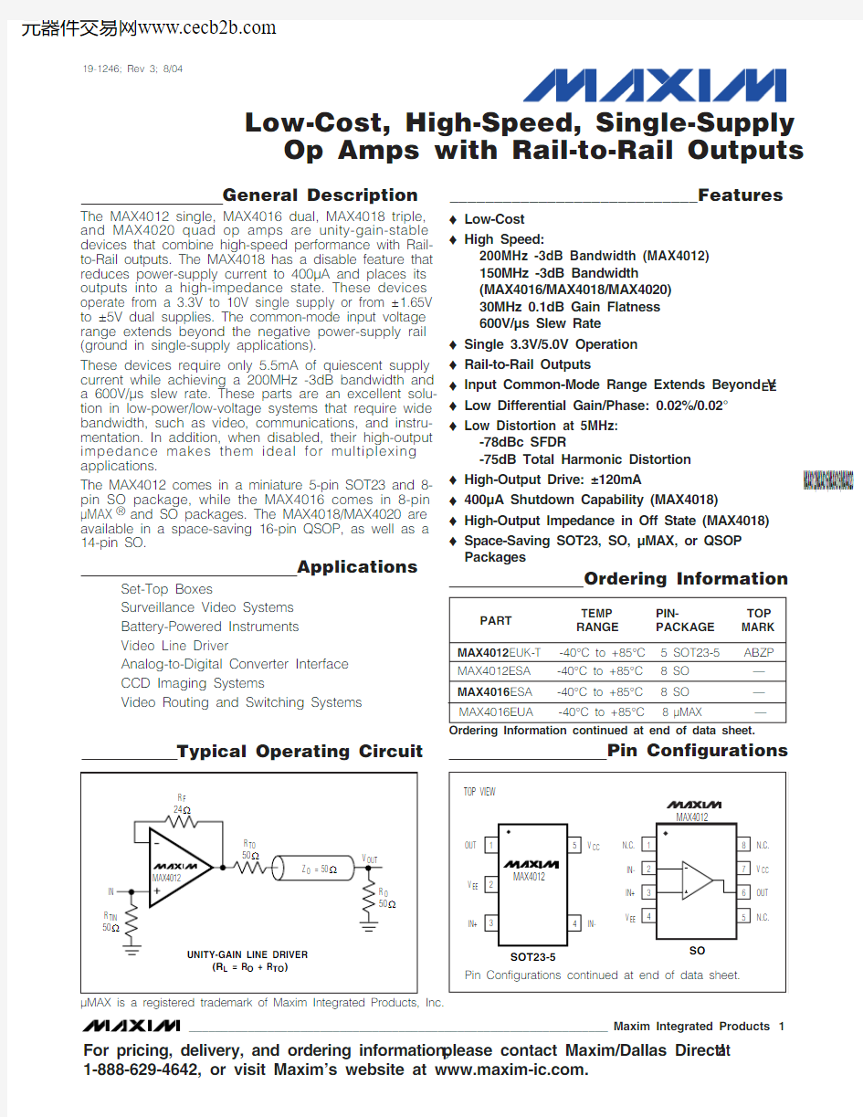
Pin Configurations
Typical Operating Circuit
19-1246; Rev 3; 8/04
For pricing, delivery, and ordering information,please contact Maxim/Dallas Direct!at 1-888-629-4642, or visit Maxim’s website at https://www.doczj.com/doc/f93246024.html,.
M A X 4012/M A X 4016/M A X 4018/M A X 4020
Low-Cost, High-Speed, Single-Supply Op Amps with Rail-to-Rail Outputs 2_______________________________________________________________________________________
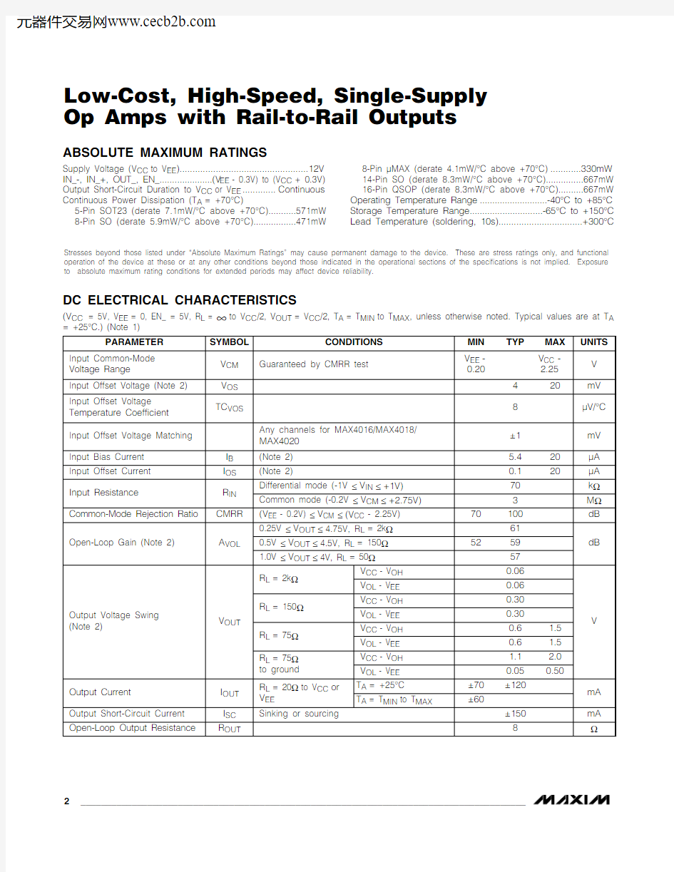
ABSOLUTE MAXIMUM RATINGS
DC ELECTRICAL CHARACTERISTICS
(V CC = 5V, V EE = 0, EN_ = 5V, R L = ∞to V CC /2, V OUT = V CC /2, T A = T MIN to T MAX , unless otherwise noted. Typical values are at T A = +25°C.) (Note 1)
Supply Voltage (V CC to V EE )..................................................12V IN_-, IN_+, OUT_, EN_.....................(V EE - 0.3V) to (V CC + 0.3V)Output Short-Circuit Duration to V CC or V EE .............Continuous Continuous Power Dissipation (T A = +70°C)
5-Pin SOT23 (derate 7.1mW/°C above +70°C)...........571mW 8-Pin SO (derate 5.9mW/°C above +70°C).................471mW
8-Pin μMAX (derate 4.1mW/°C above +70°C)............330mW 14-Pin SO (derate 8.3mW/°C above +70°C)...............667mW 16-Pin QSOP (derate 8.3mW/°C above +70°C)..........667mW Operating Temperature Range ...........................-40°C to +85°C Storage Temperature Range.............................-65°C to +150°C Lead Temperature (soldering, 10s).................................+300°C
Stresses beyond those listed under “Absolute Maximum Ratings” may cause permanent damage to the device. These are stress ratings only, and functional operation of the device at these or at any other conditions beyond those indicated in the operational sections of the specifications is not implied. Exposure to absolute maximum rating conditions for extended periods may affect device reliability.
MAX4012/MAX4016/MAX4018/MAX4020
Low-Cost, High-Speed, Single-Supply Op Amps with Rail-to-Rail Outputs
_______________________________________________________________________________________3
DC ELECTRICAL CHARACTERISTICS (continued)
(V CC = 5V, V EE = 0, EN_ = 5V, R L = ∞to V CC /2, V OUT = V CC /2, T A = T MIN to T MAX , unless otherwise noted. Typical values are at T A = +25°C.) (Note 1)
M A X 4012/M A X 4016/M A X 4018/M A X 4020
Low-Cost, High-Speed, Single-Supply Op Amps with Rail-to-Rail Outputs 4_______________________________________________________________________________________
Note 1: The MAX4012EUT is 100% production tested at T A = +25°C. Specifications over temperature limits are guaranteed by
design.
Note 2:Tested with V CM = 2.5V.
Note 3:PSR for single 5V supply tested with V EE = 0, V CC = 4.5V to 5.5V; for dual ±5V supply with V EE = -4.5V to -5.5V,
V CC = 4.5V to 5.5V; and for single 3.3V supply with V EE = 0, V CC = 3.15V to 3.45V.
Note 4: Does not include the external feedback network’s impedance.Note 5:Guaranteed by design.
AC ELECTRICAL CHARACTERISTICS
(V CC = 5V, V EE = 0, V CM = 2.5V, EN_ = 5V, R F = 24?, R L = 100?to V CC /2, V OUT = V CC /2, A VCL = 1, T A = +25°C, unless otherwise noted.)
4
-6100k 1M 10M 100M 1G
MAX4012
SMALL-SIGNAL GAIN vs. FREQUENCY
(A VCL = 1)
-4
FREQUENCY (Hz)
G A I N (d B )
-20
23-5-3-113
-7100k
1M
10M 100M
1G
MAX4016/MAX4018/MAX4020SMALL-SIGNAL GAIN vs. FREQUENCY
(A VCL = 1)
-5
FREQUENCY (Hz)
G A I N (d B )
-3-112-6
-4-209
-1
100k 1M 10M 100M 1G
MAX4012
SMALL-SIGNAL GAIN vs. FREQUENCY
(A VCL = 2)
1
FREQUENCY (Hz)
G A I N (d B )
357802469-1100k
1M
10M 100M
1G
MAX4016/MAX4018/MAX4020SMALL-SIGNAL GAIN vs. FREQUENCY
(A VCL = 2)
1
FREQUENCY (Hz)
G A I N (d B )
35780246
0.5
-0.5
0.1M
1M
10M 100M
1G MAX4016/MAX4018/MAX4020GAIN FLATNESS vs. FREQUENCY
-0.3FREQUENCY (Hz)
G A I N (d B )
-0.10.10.30.4-0.4-0.200.24
-6100k 1M 10M 100M 1G LARGE-SIGNAL GAIN vs. FREQUENCY
-4FREQUENCY (Hz)
G A I N (d B )
-20
23-5-3-110.7
-0.3
0.1M 1M 10M 100M 1G
MAX4012
GAIN FLATNESS vs. FREQUENCY
-0.1FREQUENCY (Hz)
G A I N (d B )
0.10.30.50.6-0.200.20.450-150
100k
1M
10M 100M
1G
MAX4016/MAX4018/MAX4020CROSSTALK vs. FREQUENCY
-110FREQUENCY (Hz)
C R O S S T A L K (d B )
-70-301030-130-90-50-10
1000
0.1
0.1M 1M 10M 100M
CLOSED-LOOP OUTPUT IMPEDANCE
vs. FREQUENCY
M A X 4012-09
FREQUENCY (Hz)
I M P E D A N C E (?)
100
1
10
MAX4012/MAX4016/MAX4018/MAX4020
Low-Cost, High-Speed, Single-Supply Op Amps with Rail-to-Rail Outputs
_______________________________________________________________________________________
5
Typical Operating Characteristics
(V CC = 5V, V EE = 0, A VCL = 1, R F = 24?, R L = 100?to V CC /2, T A = +25°C, unless otherwise noted.)
M A X 4012/M A X 4016/M A X 4018/M A X 4020
Low-Cost, High-Speed, Single-Supply Op Amps with Rail-to-Rail Outputs 6_______________________________________________________________________________________
0-100
100k 1M 10M 100M HARMONIC DISTORTION vs. FREQUENCY (A VCL = 1)
-80
FREQUENCY (Hz)H A R M O N I C D I S T O R T I O N (d B c )
-60-40-20-10-90-70-50-300-100
100k 1M 10M
100M
HARMONIC DISTORTION vs. FREQUENCY (A VCL = 2)
-80FREQUENCY (Hz)H A R M O N I C D I S T O R T I O N (d B c )
-60-40-20-10-90-70-50-300
-100
100k
1M
10M
100M
HARMONIC DISTORTION vs. FREQUENCY (A VCL = 5)
-80
FREQUENCY (Hz)
H A R M O N I C D I S T O R T I O N (d B c )
-60-40-20-10-90-70-50-300
-10-20-30-60-70-90
-80-40-50-100
LOAD (?)
200
400600800
1000
HARMONIC DISTORTION
vs. LOAD
H A R M O N I C D I S T O R T I O N (d B c )
0-100
100k
1M
10M
100M
COMMON-MODE REJECTION
vs. FREQUENCY
-80M A X 4012-16
FREQUENCY (Hz)
C M R (d B )
-60-40-20-10-90-70-50-300
-10-20
-30-60-70-90
-80-40
-50-100
OUTPUT SWING (Vp-p)
0.5
1.0 1.5
2.0
HARMONIC DISTORTION vs. OUTPUT SWING
H A R M O N I C D I S T O R T I O N (d B c )
-0.01
100
DIFFERENTIAL GAIN AND PHASE
-0.01
0.000.000.010.010.020.020.030.03
IRE
D I F F . P H A S
E (d e g )
D I F F . G A I N (%)
20-80
100k
1M
10M
100M
POWER-SUPPLY REJECTION
vs. FREQUENCY
-60M A X 4012-17
FREQUENCY (Hz)
P O W E R -S U P P L Y R E J E C T I O N (d B )
-40-20010-70-50-30
-10 4.5
4.03.52.52.01.53.01.0
LOAD RESISTANCE (?)
25
50
75100125150
OUTPUT SWING vs. LOAD RESISTANCE
O U T P U T S W I N G (V p -p )
Typical Operating Characteristics (continued)
(V CC = 5V, V EE = 0, A VCL = 1, R F = 24?, R L = 100?to V CC /2, T A = +25°C, unless otherwise noted.)
MAX4012/MAX4016/MAX4018/MAX4020
Low-Cost, High-Speed, Single-Supply Op Amps with Rail-to-Rail Outputs
_______________________________________________________________________________________7
IN (50mV/div)OUT (25mV/div)V O L T A G E
SMALL-SIGNAL PULSE RESPONSE
(A VCL = 1)
MAX4012-19
20ns/div
V CM = 2.5V, R L = 100? to GROUND
IN (25mV/div)OUT (25mV/div)
V O L T A G E
SMALL-SIGNAL PULSE RESPONSE
(A VCL = 2)
MAX4012-20
20ns/div
V CM = 1.25V, R L = 100? to GROUND
IN (50mV/div)OUT (25mV/div)
V O L T A G E SMALL-SIGNAL PULSE RESPONSE
(C L = 5pF, A VCL = 1)
MAX4012-21
20ns/div
V CM = 1.75V, R L = 100? to GROUND
IN (1V/div)OUT (1V/div)
V O L T A G E
LARGE-SIGNAL PULSE RESPONSE
(A VCL = 1)
MAX4012-22
20ns/div
V CM = 1.75V, R L = 100? to GROUND
100
10
1
1
10
1k
10M
1M
VOLTAGE-NOISE DENSITY
vs. FREQUENCY
M A X 4012-25
FREQUENCY (Hz)
V O L T A G E -N O I S E D E N S I T Y
100
10k
100k
IN (500mV/
div)OUT (500mV/
div)
V O L T A G E
LARGE-SIGNAL PULSE RESPONSE
(A VCL = 2)
MAX4012-23
20ns/div
V CM = 0.9V, R L = 100? to GROUND
IN (1V/div)
OUT (500mV/
div)
V O L T A G E
LARGE-SIGNAL PULSE RESPONSE
(C L = 5pF, A VCL = 2)
MAX4012-24
20ns/div
V CM = 1.75V, R L = 100? to GROUND
10
1
1
10
1k
10M
1M
CURRENT-NOISE DENSITY
vs. FREQUENCY
M A X 4012-26
FREQUENCY (Hz)
C U R R E N T -N O I S E
D
E N S I T Y
100
10k
100k
EN_
5.0V (ENABLE)
(DISABLE)
1V
OUT ENABLE RESPONSE TIME
MAX4012-27
1μs/div
V IN = 1.0V
Typical Operating Characteristics (continued)
(V CC = 5V, V EE = 0, A VCL = 1, R F = 24?, R L = 100?to V CC /2, T A = +25°C, unless otherwise noted.)
M A X 4012/M A X 4016/M A X 4018/M A X 4020
Low-Cost, High-Speed, Single-Supply Op Amps with Rail-to-Rail Outputs 8_______________________________________________________________________________________
7050
6040
30
20
M A X 4012-28
LOAD RESISTANCE (?)
200
400600800
1k
OPEN-LOOP GAIN vs. LOAD RESISTANCE
O P E N -L O O P G A I N (d B )
40035030025015050
1002000M A X 4012-29
LOAD RESISTANCE (?)
100
200500400300600
CLOSED-LOOP BANDWIDTH vs. LOAD RESISTANCE
C L O S E
D -L O O P B A N D W I D T H (M H z )
10
-90
100k
10M
100M
1M
OFF-ISOLATION vs. FREQUENCY
-80M A X 4012-30
FREQUENCY (Hz)
O F F -I S O L A T I O N (d B )
-70-60-50-40-30-20-100 7
6
453M A X 4012-31
TEMPERATURE (°C)
-25
-50
075
5025100
SUPPLY CURRENT vs. TEMPERATURE
S U P P L Y C U R R E N T (m A )
10
86
4
2
0M A X 4012-34
SUPPLY VOLTAGE (V)
4
3
5
678910
11
SUPPLY CURRENT vs. SUPPLY VOLTAGE
S U P P L Y C U R R E N T (m A )
6.0
5.5
4.5
5.0
4.0
M A X 4012-32
TEMPERATURE (°C)
-25
-50
075
5025100
INPUT BIAS CURRENT vs. TEMPERATURE
I N P U T B I A S C U R R E N T (μA )
0.20
0.16
0.12
0.04
0.08
0M A X 4012-33
TEMPERATURE (°C)
-25
-50
075
5025100
INPUT OFFSET CURRENT vs. TEMPERATURE
I N P U T O F F S E T V O L T A G E
5
4
3
1
2
0M A X 4012-35
TEMPERATURE (°C)
-25
-50
075
5025100
INPUT OFFSET VOLTAGE vs. TEMPERATURE
I N P U T O F F S E T V O L T A G E (m V )
5.0
4.8
4.6
4.2
4.4
4.0
TEMPERATURE (°C)
-25
-50
075
5025100
OUTPUT VOLTAGE SWING vs. TEMPERATURE
O U T P U T V O L T A G E S W I N G (V p -p )
Typical Operating Characteristics (continued)
(V CC = 5V, V EE = 0, A VCL = 1, R F = 24?, R L = 100?to V CC /2, T A = +25°C, unless otherwise noted.)
MAX4012/MAX4016/MAX4018/MAX4020
Low-Cost, High-Speed, Single-Supply Op Amps with Rail-to-Rail Outputs
_______________________________________________________________________________________9
Pin Description
M A X 4012/M A X 4016/M A X 4018/M A X 4020
Detailed Description
The MAX4012/MAX4016/MAX4018/MAX4020 are sin-gle-supply, rail-to-rail, voltage-feedback amplifiers that employ current-feedback techniques to achieve 600V/μs slew rates and 200MHz bandwidths. Excellent harmonic distortion and differential gain/phase perfor-mance make these amplifiers an ideal choice for a wide variety of video and RF signal-processing applications.The output voltage swing comes to within 50mV of each supply rail. Local feedback around the output stage assures low open-loop output impedance to reduce gain sensitivity to load variations. This feedback also produces demand-driven current bias to the output transistors for ±120mA drive capability, while constrain-ing total supply current to less than 7mA. The input stage permits common-mode voltages beyond the nega-tive supply and to within 2.25V of the positive supply rail.
Applications Information
Choosing Resistor Values
Unity-Gain Configuration
The MAX4012/MAX4016/MAX4018/MAX4020 are inter-nally compensated for unity gain. When configured for unity gain, the devices require a 24?resistor (R F ) in series with the feedback path. This resistor improves AC response by reducing the Q of the parallel LC cir-
cuit formed by the parasitic feedback capacitance and inductance.
Inverting and Noninverting Configurations
Select the gain-setting feedback (R F ) and input (R G )resistor values to fit your application. Large resistor val-ues increase voltage noise and interact with the amplifi-er’s input and PC board capacitance. This can generate undesirable poles and zeros and decrease bandwidth or cause oscillations. For example, a nonin-verting gain-of-two configuration (R F = R G ) using 1k ?resistors, combined with 1pF of amplifier input capaci-tance and 1pF of PC board capacitance, causes a pole at 159MHz. Since this pole is within the amplifier band-width, it jeopardizes stability. Reducing the 1k ?resis-tors to 100?extends the pole frequency to 1.59GHz,but could limit output swing by adding 200?in parallel with the amplifier’s load resistor. Table 1 shows sug-gested feedback, gain resistors, and bandwidth for several gain values in the configurations shown in Figures 1a and 1b.
Layout and Power-Supply Bypassing
These amplifiers operate from a single 3.3V to 11V power supply or from dual supplies to ±5.5V. For single-supply operation, bypass V CC to ground with a 0.1μF capacitor as close to the pin as possible. If operating with dual sup-plies, bypass each supply with a 0.1μF capacitor.
Low-Cost, High-Speed, Single-Supply Op Amps with Rail-to-Rail Outputs 10______________________________________________________________________________________
Figure 1a. Noninverting Gain Configuration Figure 1b. Inverting Gain Configuration
Maxim recommends using microstrip and stripline tech-niques to obtain full bandwidth. To ensure that the PC board does not degrade the amplifier’s performance,design it for a frequency greater than 1GHz. Pay care-ful attention to inputs and outputs to avoid large para-sitic capacitance. Whether or not you use a constant-impedance board, observe the following guidelines when designing the board:
?Don’t use wire-wrap boards because they are too inductive.
?Don’t use IC sockets because they increase parasitic capacitance and inductance.
?Use surface-mount instead of through-hole compo-nents for better high-frequency performance.
?Use a PC board with at least two layers; it should be as free from voids as possible.
?Keep signal lines as short and as straight as possi-ble. Do not make 90°turns; round all corners.
Rail-to-Rail Outputs, Ground-Sensing Input
The input common-mode range extends from (V EE - 200mV) to (V CC - 2.25V) with excellent common-mode rejection. Beyond this range, the amplifier output is a nonlinear function of the input, but does not under-go phase reversal or latchup.
The output swings to within 60mV of either power-supply rail with a 2k ?load. The input ground-sensing and the rail-to-rail output substantially increase the dynamic range. With a symmetric input in a single 5V application, the input can swing 2.95V P-P , and the out-put can swing 4.9V P-P with minimal distortion.
Enable Input and Disabled Output
The enable feature (EN_) allows the amplifier to be placed in a low-power, high-output-impedance state.Typically, the EN_ logic low input current (I IL ) is small.However, as the EN voltage (V IL ) approaches the nega-tive supply rail, I IL increases (Figure 2). A single resis-tor connected as shown in Figure 3 prevents the rise in the logic-low input current. This resistor provides a feedback mechanism that increases V IL as the logic input is brought to V EE . Figure 4 shows the resulting input current (I IL ).
When the MAX4018 is disabled, the amplifier’s output impedance is 35k ?. This high resistance and the low 2pF output capacitance make this part ideal in RF/video multiplexer or switch applications. For larger arrays, pay careful attention to capacitive loading. See the Output Capacitive Loading and Stability section for more information.
MAX4012/MAX4016/MAX4018/MAX4020
Low-Cost, High-Speed, Single-Supply Op Amps with Rail-to-Rail Outputs
______________________________________________________________________________________11
Table 1. Recommended Component Values
Note:R L = R O + R TO ; R TIN and R TO are calculated for 50?applications. For 75?systems, R TO = 75?; calculate R TIN from the
following equation:
R =
75
1-75R TIN G
?
M A X 4012/M A X 4016/M A X 4018/M A X 4020
To implement the mux function, the outputs of multiple amplifiers can be tied together, and only the amplifier with the selected input will be enabled. All of the other amplifiers will be placed in the low-power shutdown mode, with their high output impedance presenting very little load to the active amplifier output. For gains of +2 or greater, the feedback network impedance of all the amplifiers used in a mux application must be considered when calculating the total load on the active amplifier output
Output Capacitive Loading and Stability
The MAX4012/MAX4016/MAX4018/MAX4020 are opti-mized for AC performance. They are not designed to drive highly reactive loads, which decreases phase margin and may produce excessive ringing and oscilla-tion. Figure 5 shows a circuit that eliminates this prob-lem. Figure 6 is a graph of the optimal isolation resistor (R S ) vs. capacitive load. Figure 7 shows how a capaci-tive load causes excessive peaking of the amplifier’s frequency response if the capacitor is not isolated from the amplifier by a resistor. A small isolation resistor (usually 20?to 30?) placed before the reactive load prevents ringing and oscillation. At higher capacitive loads, AC performance is controlled by the interaction of the load capacitance and the isolation resistor.Figure 8 shows the effect of a 27?isolation resistor on closed-loop response.
Coaxial cable and other transmission lines are easily driven when properly terminated at both ends with their characteristic impedance. Driving back-terminated transmission lines essentially eliminates the line’s capacitance.
Low-Cost, High-Speed, Single-Supply Op Amps with Rail-to-Rail Outputs 12______________________________________________________________________________________
Figure 2. Enable Logic-Low Input Current vs. V IL
Figure 4. Enable Logic-Low Input Current vs. V IL with 10k ?Series Resistor
Figure 3. Circuit to Reduce Enable Logic-Low Input Current
MAX4012/MAX4016/MAX4018/MAX4020
Low-Cost, High-Speed, Single-Supply Op Amps with Rail-to-Rail Outputs
______________________________________________________________________________________13
Figure 5. Driving a Capacitive Load through an Isolation Resistor
Figure 7. Small-Signal Gain vs. Frequency with Load Capacitance and No Isolation Resistor Figure 8. Small-Signal Gain vs. Frequency with Load Capacitance and 27?Isolation Resistor
M A X 4012/M A X 4016/M A X 4018/M A X 4020
Low-Cost, High-Speed, Single-Supply Op Amps with Rail-to-Rail Outputs 14______________________________________________________________________________________
Pin Configurations (continued)
MAX4012/MAX4016/MAX4018/MAX4020
Low-Cost, High-Speed, Single-Supply Op Amps with Rail-to-Rail Outputs
______________________________________________________________________________________15
___________________Chip Information
Ordering Information (continued)
MAX4012 TRANSISTOR COUNT: 95MAX4016 TRANSISTOR COUNT: 190MAX4018 TRANSISTOR COUNT: 299MAX4020 TRANSISTOR COUNT: 362
Package Information
(The package drawing(s) in this data sheet may not reflect the most current specifications. For the latest package outline information go to https://www.doczj.com/doc/f93246024.html,/packages .)
M A X 4012/M A X 4016/M A X 4018/M A X 4020
Low-Cost, High-Speed, Single-Supply Op Amps with Rail-to-Rail Outputs 16______________________________________________________________________________________
Package Information (continued)
(The package drawing(s) in this data sheet may not reflect the most current specifications. For the latest package outline information go to https://www.doczj.com/doc/f93246024.html,/packages .)
Maxim cannot assume responsibility for use of any circuitry other than circuitry entirely embodied in a Maxim product. No circuit patent licenses are implied. Maxim reserves the right to change the circuitry and specifications without notice at any time.
17____________________Maxim Integrated Products, 120 San Gabriel Drive, Sunnyvale, CA 94086 408-737-7600?2004 Maxim Integrated Products
Printed USA
is a registered trademark of Maxim Integrated Products.
MAX4012/MAX4016/MAX4018/MAX4020
Low-Cost, High-Speed, Single-Supply Op Amps with Rail-to-Rail Outputs
Package Information (continued)
(The package drawing(s) in this data sheet may not reflect the most current specifications. For the latest package outline information go to https://www.doczj.com/doc/f93246024.html,/packages .)