
MC14598B
8-Bit Bus-Compatible Latches
The MC14598B is an 8–bit latch addressed with an external binary address. The 8 latch–outputs are high drive, three–state and bus line compatible. The drive capability allows direct applications with MPU systems such as the Motorola 6800 family.
The latches of the MC14598B are accessed via the Address pins,A0, A1, and A2.
All 8 outputs from the latches are available in parallel when Enable is in the low state. Data is entered into a selected latch from the Data pin when the Strobe is high. Master reset is available on both parts.
?Serial Data Input
?Three–State Bus Compatible Parallel Outputs
?Three–State Control Pin (Enable) TTL Compatible Input ?Open Drain Full Flag (Multiple Latch Wire–O Ring)?Master Reset
?Level Shifting Inputs on All Except Enable ?Diode Protection — All Inputs
?Supply V oltage Range — 3.0 Vdc to 18 Vdc
?
Capable of Driving TTL Over Rated Temperature Range With Fanout as Follows:
1 TTL Load 4 LSTTL Loads
MAXIMUM RATINGS (Voltages Referenced to V
) (Note 1.)
1.Maximum Ratings are those values beyond which damage to the device may occur.
2.Temperature Derating:
Plastic “P and D/DW” Packages: – 7.0 mW/_C From 65_C To 125_C
https://www.doczj.com/doc/f7565161.html,
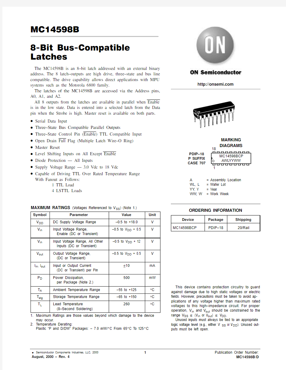
Device Package Shipping ORDERING INFORMATION
MC14598BCP
PDIP–18
20/Rail
This device contains protection circuitry to guard against damage due to high static voltages or electric fields. However, precautions must be taken to avoid ap-plications of any voltage higher than maximum rated voltages to this high–impedance circuit. For proper operation, V in and V out should be constrained to the range V SS v (V in or V out ) v V DD .
Unused inputs must always be tied to an appropriate logic voltage level (e.g., either V SS or V DD ). Unused out-puts must be left open.
NC DATA RESET D0V SS
A1A0STROBE
ENABLE
D3D2D1V DD A2
D7D6D5D4
BLOCK DIAGRAMS
MC14598B
D n = State of nth latch
OUTPUT NC = NO CONNECTION
D0D1D2D3D4D5D6D7
ENABLE
4.The formulas given are for the typical characteristics only at 25_C.
6.Data labelled “Typ” is not to be used for design purposes but is intended as an indication of the IC’s potential performance.
MC14598B FUNCTION DIAGRAM
ENABLE?4
RESET?21?D0
17?D116?D215?D314?D413?D512?D611?D7
(M.S.B)
MC14598B TIMING DIAGRAM
*1.4 V with V DD = 5.0 V NOTES:
1.High–impedance output state (another device controls bus).
2.Output Load as for MC14597B.
D7RESET A0, A1, A2
DATA STROBE ENABLE
t
X = Don’t care TEST LOAD ALL OUTPUTS
D n L = 2.5 k
Circuit diagrams external to or containing Motorola products are included as a means of illustration https://www.doczj.com/doc/f7565161.html,plete information sufficient for construction purposes may not be fully illustrated. Although the information herein has been carefully checked and is believed to be reliable.Motorola assumes no responsibility for https://www.doczj.com/doc/f7565161.html,rmation herein does not convey to the purchaser any license under the patent rights of Motorola or others.
The information contained herein is for guidance only,with no warranty of any type, expressed or implied.Motorola reserves the right to make any changes to the information and the product(s) to which the information applies and to discontinue manufacture of the product(s) at any time.
PACKAGE DIMENSIONS
PDIP–18P SUFFIX
PLASTIC DIP PACKAGE
CASE 707–02ISSUE C
NOTES:
1.POSITIONAL TOLERANCE OF LEADS (D),SHALL BE WITHIN 0.25 (0.010) AT MAXIMUM MATERIAL CONDITION, IN RELATION TO SEATING PLANE AND EACH OTHER.
2.DIMENSION L TO CENTER OF LEADS WHEN FORMED PARALLEL.
3.DIMENSION B DOES NOT INCLUDE MOLD FLASH.
4.CONTROLLING DIMENSION: INCH.
DIM MIN MAX MIN MAX MILLIMETERS
INCHES A 22.2223.240.8750.915B 6.10 6.600.2400.260C 3.56 4.570.1400.180D 0.360.560.0140.022F 1.27 1.780.0500.070G 2.54 BSC 0.100 BSC H 1.02 1.520.0400.060J 0.200.300.0080.012K 2.92 3.430.1150.135L 7.62 BSC 0.300 BSC M 0 15 0 15 N
0.51 1.02
0.0200.040
____
ON Semiconductor and are trademarks of Semiconductor Components Industries, LLC (SCILLC). SCILLC reserves the right to make changes without further notice to any products herein. SCILLC makes no warranty, representation or guarantee regarding the suitability of its products for any particular purpose, nor does SCILLC assume any liability arising out of the application or use of any product or circuit, and specifically disclaims any and all liability, including without limitation special, consequential or incidental damages. “Typical” parameters which may be provided in SCILLC data sheets and/or specifications can and do vary in different applications and actual performance may vary over time. All operating parameters, including “Typicals” must be validated for each customer application by customer’s technical experts. SCILLC does not convey any license under its patent rights nor the rights of others.
SCILLC products are not designed, intended, or authorized for use as components in systems intended for surgical implant into the body, or other applications intended to support or sustain life, or for any other application in which the failure of the SCILLC product could create a situation where personal injury or death may occur. Should Buyer purchase or use SCILLC products for any such unintended or unauthorized application, Buyer shall indemnify and hold SCILLC and its officers, employees, subsidiaries, affiliates, and distributors harmless against all claims, costs, damages, and expenses, and reasonable attorney fees arising out of, directly or indirectly, any claim of personal injury or death associated with such unintended or unauthorized use, even if such claim alleges that SCILLC was negligent regarding the design or manufacture of the part. SCILLC is an Equal Opportunity/Affirmative Action Employer. PUBLICATION ORDERING INFORMATION
CENTRAL/SOUTH AMERICA:
Spanish Phone:303–308–7143 (Mon–Fri 8:00am to 5:00pm MST)
Email:ONlit–spanish@https://www.doczj.com/doc/f7565161.html,
ASIA/PACIFIC: LDC for ON Semiconductor – Asia Support
Phone:303–675–2121 (Tue–Fri 9:00am to 1:00pm, Hong Kong Time)
Toll Free from Hong Kong & Singapore:
001–800–4422–3781
Email: ONlit–asia@https://www.doczj.com/doc/f7565161.html,
JAPAN: ON Semiconductor, Japan Customer Focus Center
4–32–1 Nishi–Gotanda, Shinagawa–ku, Tokyo, Japan 141–0031
Phone: 81–3–5740–2745
Email: r14525@https://www.doczj.com/doc/f7565161.html,