P06P03LVG中文资料
- 格式:pdf
- 大小:359.35 KB
- 文档页数:5
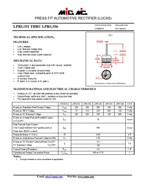
VOLTAGE RANGE 100 to 600 Volts LPRG351 THRU LPRG356CURRENT35.0 AmperesTECHNICAL SPECIFICATION : FEATURES• Low Leakage• Low forward voltage drop • High current capability•High forward surge current capacityMECHANICAL DATA• Technology: Glass passivated chip with vacuum soldered • Case: Copper case• Polarity: As marked of case bottom• Lead: Plated lead , solderable per MIL-STD-202E method 208C• Mounting: Press Fit•Weight: 0.21 ounces, 6.01 gramsMAXIMUM RATINGS AND ELECTRICAL CHARACTERISTICS• Ratings at 25℃ ambient temperature unless otherwise specified • Single Phase, half wave, 60HZ, resistive or inductive load •For capacitive load derate current by 20%SYMBOLS LPRG351 LPRG352 LPRG353 LPRG354 LPRG356 UNIT Maximum Repetitive Peak Reverse Voltage V RRM 100 200 300 400 600 Volts Maximum RMS Voltage V RMS 70 140 210 280 420 Volts Maximum DC Blocking VoltageV DC 100200300 400600Volts Maximum Average Forward Rectified Current, At Tc=105℃I (AV)35AmpsPeak Forward Surge Current3.3mS single half sine wave superimposed on Rated load (JEDEC method) I FSM 500 Amps Rating for fusing (t <8.3ms)I 2t 1038 A 2S Maximum instantaneous Forward Voltage at 100A V F 1.08 Volts 5.0 Maximum DC Reverse Current at Rated TA=25℃ DC Blocking Voltage TA=100℃ I R 450 UA Typical Thermal ResistanceR θJC 0.8 ℃/W Operating and Storage Temperature RangeT J ,T STG(-65 to +175)℃Notes:1. Enough heatsink must be considered in application.VOLTAGE RANGE 100 to 600 Volts LPRG351 THRU LPRG356CURRENT35.0 AmperesRATINGS AND CHARACTERISTIC CURVES LPRG351 THRULPRG356F1G.2 MAXIMUM NON-REPETITIVE PEAKFORWARD SURGE CURRENTF1G.1 TYPICAL FORWARD CURRENTDERATING GURVENUMBER OF CYCLES AT 60 Hz1006040201086421P E A K F O R W A R D S U R G E C U R R E N T ,(A )A V E R A G E F O R W A R D C U R R E N T ,(A )AMBIENT TEMPERATURE, ()℃12510015017575502500.11.0101000INSTANTANEOUS FORWARD VOLTAGE,(V)I N S T A N T A N E O U S F O R W A R D C U R R E N T ,(A )F1G.3 TYPICAL INSTANTANEOUS FORWARD CHARACTERISTICS80402050403020100604020A V E R A G E P O W E R D I S S I P A T I O N (W )AVERAGE FORWARD CURRENT, (A)F1G.4 FORWARD ROWER DISSIPATION3010。
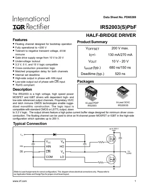
Data Sheet No. PD60269Typical ConnectionProduct SummaryV OFFSET 200 V max.I O +/-130 mA/270 mA V OUT 10 V - 20 V t on/off (typ.)680 ns/150 nsDeadtime (typ.)520 nsHALF-BRIDGE DRIVERFeatures•Floating channel designed for bootstrap operation •Fully operational to +200 V•Tolerant to negative transient voltage, dV/dtimmune•Gate drive supply range from 10 V to 20 V •Undervoltage lockout•3.3 V, 5 V, and 15 V logic compatible •Cross-conduction prevention logic•Matched propagation delay for both channels •Internal set deadtime•High -side output in phase with HIN input •Low -side output out of phase with LIN input DescriptionThe IRS2003 is a high voltage, high speed power MOSFE T and IGBT drivers wi th dependent high - and low -side referenced output channels. Proprietary HVICand latch immune CMOS technologies enable rugge-dized monolithic construction. The logic input iscompatible with standard CMOS or LSTTL output, downto 3.3 V logic. The output drivers feature a high pulse current buffer stage designed for minimum driver cross-conduction. The floating channel can be used to drive an N-channel power MOSFET or IGBT in the high -side configuration which operates up to 200 V. 1IRS2003(S)PbFPackages8-Lead PDIP IRS20038-Lead SOIC IRS2003S • RoHS compliantIRS2003(S)PbFAbsolute Maximum RatingsAbsolute maximum ratings indicate sustained limits beyond which damage to the device may occur. All voltage param-eters are absolute voltages referenced to COM. The thermal resistance and power dissipation ratings are measured under board mounted and still air conditions.Note 1: Logic operational for V S of -5 V to +200 V. Logic state held for V S of -5 V to -V BS . (Please refer to the Design Tip DT97-3 for more details).IRS2003(S)PbFStatic Electrical CharacteristicsV BIAS (V CC, V BS) = 15 V and T A = 25 °C unless otherwise specified. The V IN, V TH, and I IN parameters are referenced to COM. The V O and I O parameters are referenced to COM and are applicable to the respective output leads: HO or LO. Dynamic Electrical CharacteristicsV BIAS (V CC, V BS) = 15 V, C L = 1000 pF and T A = 25 °C unless otherwise specified.IRS2003(S)PbFLead DefinitionsSymbol DescriptionHIN Logic input for high -side gate driver output (HO), in phase Logic input for low-side gate driver output (LO), out of phase V B High -side floating supply HO High -side gate drive output V S High -side floating supply return V CC Low-side and logic fixed supply LO Low -side gate drive output COMLow -side returnLIN Lead Assignments8 Lead PDIP 8 Lead SOICIRS2003PbF IRS2003SPbF12348765V CC HIN LIN COMV B HO V S LO12348765V CC HIN LIN COMV B HO V S LOIRS2003(S)PbFLINHOLOHINFigure 3. Deadtime Waveform DefinitionsFigure 2. Switching Time Waveform DefinitionsLOIRS2003(S)PbFIRS2003(S)PbF8-50-250255075100125Temperature (oC)Figure 10A. Logic "0"(HIN) & Logic "1" ( )Input Voltage vs. TemperatureLINIRS2003(S)PbFIRS2003(S)PbFIRS2003(S)PbF10vs. Temperaturevs. VoltageFigure 17A. Logic "0" Input Bias Currentvs. TemperatureFigure 17B. Logic "0" Input Bias Currentvs. VoltageL o g i c “0” I n p u t B i a s C u r r e n t (µA )0123456-50-250255075100125Temperature (°C)F ig u r e 17A. L o g ic "0" I n p u t B ia s C u r r e n t 0123456101214161820Supply Voltage (V)Case OutlinesCTape & Reel 8-lead SOICPer SCOP 200-002The SOIC-8 is MSL 2 qualified.This product has been designed and qualified for the industrial level.Qualification standards can be found at Data and specifications subject to change without notice. 11/27/2006。
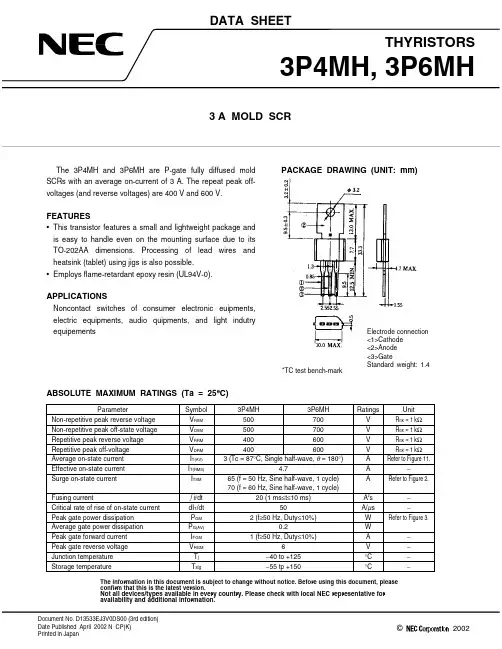
1998©Document No. D13533EJ3V0DS00 (3rd edition)Date Published April 2002 N CP(K)Printed in JapanTHYRISTORS3P4MH, 3P6MH3 A MOLD SCRDATA SHEET2002The information in this document is subject to change without notice. Before using this document, please confirm that this is the latest version.Not all devices/types available in every country. Please check with local NEC representative for availability and additional information.The 3P4MH and 3P6MH are P-gate fully diffused mold SCRs with an average on-current of 3 A. The repeat peak off-voltages (and reverse voltages) are 400 V and 600 V.FEATURES•This transistor features a small and lightweight package and is easy to handle even on the mounting surface due to its TO-202AA dimensions. Processing of lead wires and heatsink (tablet) using jigs is also possible.•Employs flame-retardant epoxy resin (UL94V-0).APPLICATIONSNoncontact switches of consumer electronic euipments,electric equipments, audio quipments, and light indutry equipementsPACKAGE DRAWING (UNIT: mm)ABSOLUTE MAXIMUM RATINGS (Ta = 25°C)ParameterSymbol 3P4MH3P6MHRatings Unit Non-repetitive peak reverse voltage V RSM 500700V R GK = 1 k ΩNon-repetitive peak off-state voltage V DSM 500700V R GK = 1 k ΩRepetitive peak reverse voltage V RRM 400600V R GK = 1 k ΩRepetitive peak off-voltage V DRM 400600V R GK = 1 k ΩAverage on-state current I T(AV) 3 (Tc = 87°C, Single half-wave, θ = 180°)A Refer to Figure 11.Effective on-state current I T(RMS) 4.7A −Surge on-state currentI TSM65 (f = 50 Hz, Sine half-wave, 1 cycle)70 (f = 60 Hz, Sine half-wave, 1 cycle)A Refer to Figure 2.Fusing current∫ i t 2dt 20 (1 ms ≤t ≤10 ms)A 2s −Critical rate of rise of on-state current dI T /dt 50A/µs −Peak gate power dissipation P GM 2 (f ≥50 Hz, Duty ≤10%)W Refer to Figure 3.Average gate power dissipation P G(AV)0.2W Peak gate forward current I FGM 1 (f ≥50 Hz, Duty ≤10%)A −Peak gate reverse voltage V RGM 6V −Junction temperature T j −40 to +125°C −Storage temperatureT stg−55 tp +150°C−Electrode connection <1>Cathode <2>Anode <3>GateStandard weight: 1.4*TC test bench-markData Sheet D13533EJ3V0DS2ELECTRICAL CHARACTERISTICS (T j = 25°C, R GK = 1 k Ω)TYPICAL CHARACTERISTICS (Ta = 25°C)Data Sheet D13533EJ3V0DS34Data Sheet D13533EJ3V0DS[MEMO]Data Sheet D13533EJ3V0DS5M8E 00. 4The information in this document is current as of July, 2001. The information is subject to change without notice. For actual design-in, refer to the latest publications of NEC's data sheets or data books, etc., for the most up-to-date specifications of NEC semiconductor products. Not all products and/or types are available in every country. Please check with an NEC sales representative for availability and additional information.No part of this document may be copied or reproduced in any form or by any means without prior written consent of NEC. NEC assumes no responsibility for any errors that may appear in this document.NEC does not assume any liability for infringement of patents, copyrights or other intellectual property rights of third parties by or arising from the use of NEC semiconductor products listed in this document or any other liability arising from the use of such products. No license, express, implied or otherwise, is granted under any patents, copyrights or other intellectual property rights of NEC or others.Descriptions of circuits, software and other related information in this document are provided for illustrative purposes in semiconductor product operation and application examples. The incorporation of these circuits, software and information in the design of customer's equipment shall be done under the full responsibility of customer. NEC assumes no responsibility for any losses incurred by customers or third parties arising from the use of these circuits, software and information.While NEC endeavours to enhance the quality, reliability and safety of NEC semiconductor products, customers agree and acknowledge that the possibility of defects thereof cannot be eliminated entirely. To minimize risks of damage to property or injury (including death) to persons arising from defects in NEC semiconductor products, customers must incorporate sufficient safety measures in their design, such as redundancy, fire-containment, and anti-failure features.NEC semiconductor products are classified into the following three quality grades:"Standard", "Special" and "Specific". The "Specific" quality grade applies only to semiconductor products developed based on a customer-designated "quality assurance program" for a specific application. The recommended applications of a semiconductor product depend on its quality grade, as indicated below. Customers must check the quality grade of each semiconductor product before using it in a particular application."Standard":Computers, office equipment, communications equipment, test and measurement equipment, audioand visual equipment, home electronic appliances, machine tools, personal electronic equipment and industrial robots"Special":Transportation equipment (automobiles, trains, ships, etc.), traffic control systems, anti-disastersystems, anti-crime systems, safety equipment and medical equipment (not specifically designed for life support)"Specific":Aircraft, aerospace equipment, submersible repeaters, nuclear reactor control systems, lifesupport systems and medical equipment for life support, etc.The quality grade of NEC semiconductor products is "Standard" unless otherwise expressly specified in NEC's data sheets or data books, etc. If customers wish to use NEC semiconductor products in applications not intended by NEC, they must contact an NEC sales representative in advance to determine NEC's willingness to support a given application.(Note)(1)"NEC" as used in this statement means NEC Corporation and also includes its majority-owned subsidiaries.(2)"NEC semiconductor products" means any semiconductor product developed or manufactured by or forNEC (as defined above).••••••。
Product information is current as of publication date. The product conforms Copyright © 2006, 2007, Pletronics Inc.LV77D Series 3.3 VLVDS Clock Oscillators April 2007•Pletronics’ LV77D Series is a quartz crystalcontrolled precision square wave generator with an LVDS output.•The package is designed for high density surface mount designs.•Low cost mass produced oscillator.•Tape and Reel or cut tape packaging is available.• 5 x 7 mm LCC Ceramic Package •Enable/Disable Function on pad 1•Disable function includes low standby power mode •Low JitterPletronics Inc. certifies this device is in accordance with the RoHS 6/6 (2002/95/EC) and WEEE (2002/96/EC) directives.Pletronics Inc. guarantees the device does not contain the following:Cadmium, Hexavalent Chromium, Lead, Mercury, PBB’s, PBDE’s Weight of the Device: 0.16 gramsMoisture Sensitivity Level: 1 As defined in J-STD-020C Second Level Interconnect code: e4Absolute Maximum Ratings:ParameterUnitV CC Supply Voltage -0.5V to +5.0V Vi Input Voltage -0.5V to V CC + 0.5V Vo Output Voltage-0.5V to V CC + 0.5VThermal CharacteristicsThe maximum die or junction temperature is 155o CThe thermal resistance junction to board is 30 to 50o C/Watt depending on the solder pads, ground plane and construction of the PCB.April 2007Part Number:LV7745DEV-125.0M-XXPart Marking:PLE LV77FF.FFF M C YMDXX orLV7XYWWXX FF.FFF M C PLE XXXPackaging code or blank T250 = 250 per Tape and Reel T500 = 500 per Tape and Reel T1K = 1000 per Tape and Reel Frequency in MHz Supply Voltage V CC V = 3.3V +_ 10%Optional Enhanced OTRBlank = Temp. range -10 to +70o C E = Temp. range -40 to +85o C Series Model Frequency Stability 45 = +_ 50 ppm 44 = +_ 25 ppm 20 = +_ 20 ppm Series ModelMarking Legend:PLE = PletronicsFF.FFF M = Frequency in MHzYYWW or YWW or YMD = Date of Manufacture (year and week, or year-month-day)All other marking is internal factory codes Specifications such as frequency stability, supply voltage and operating temperature range, etc. arenot identified from the marking. External packaging labels and packing list will correctly identify the ordered Pletronics part number.Codes for Date Code YMDCode 6789012Year 2006200720082009201020112012Code A B C D E F G H J K L M Month JANFEBMARAPRMAY JUN JUL AUG SEP OCT NOV DEC Code 123456789A B C Day 123456789101112Code D E F G H J K L M N P R Day 131415161718192021222324Code T U V W X Y Z Day25262728293031April 2007Electrical Specification for 3.30V +_10% over the specified temperature range andthe frequency range of 1 to 250 MHzItemMin Max Unit ConditionFrequency Accuracy “45"-50+50ppmFor all supply voltages, load changes, aging for 1year, shock, vibration and temperatures“44"-25+25 “20"-20+20Output Waveform LVDS Output High Level -- 1.60Volts -See load circuit R1 = 50 ohmsOutput Low Level 0.90--Volts -Differential Output (V OD )250450mVolts -Output Offset Voltage (V OS ) 1.125 1.375Volts > 80 MHz 1.125 1.500Volts < 80 MHz Differential Output Error (dV OS )--50mVolts -Output Symmetry 4555%Referenced to 50% of amplitude or crossing point Output T RISE and T FALL 300700pS > 80 MHz Vth is 20% and 80% of waveform 400900pS < 80 MHzJitter-0.6pS RMSMeasured from 12KHz to 20MHz from Fnominal - 2.8Measured from 10Hz to 1MHz from Fnominal Vcc Supply Current-66mA > 80 MHz Includes current of properly terminated device-45mA < 80 MHzEnable/Disable Internal Pull-up 50-Kohm To Vcc (equivalent resistance)V disable -0.8Volts Referenced to Ground V enable2.0-Volts Referenced to Ground Output leakage V OUT = V CC -10+10uA Pad 1 low, device disabledV OUT = 0V -10+10uA Enable -10nS Time for output to reach a logic state Disable time -10nS Time for output to reach a high Z state Start up time-5mS > 80 MHz Measured from the time Vcc = 3.0V-3mS< 80 MHzOperating Temperature Range-10+70o C Standard Temperature Range-40+85o C Extended Temperature Range “E ” OptionStorage Temperature Range -55+125oCStandby Current I CC-3uA> 80 MHz Pad 1 low, device disabled- 1.5mA< 80 MHzSpecifications with Pad 1 E/D open circuitApril 2007-160-140-120-100-80-60-40-200101,000100,00010,000,000Frequency (Hz)d B c /HzTypical Phase-Noise ResponseLoad CircuitApril 2007Reliability:Environmental ComplianceParameter ConditionMechanical Shock MIL-STD-883 Method 2002, Condition BVibration MIL-STD-883 Method 2007, Condition ASolderability MIL-STD-883 Method 2003Thermal Shock MIL-STD-883 Method 1011, Condition AESD RatingModel Minimum Voltage ConditionsHuman Body Model1500MIL-STD-883 Method 3115Charged Device Model1000JESD 22-C101Package LabelingLabel is 1" x 2.6" (25.4mm x 66.7mm)Label is 1" x 2.6" (25.4mm x 66.7mm) Font is Courier New Font is ArialBar code is 39-Full ASCIIApril 2007Inches mm A 0.276 +_0.0067.00 +_0.15B 0.197 +_0.006 5.00 +_0.15C 0.067 max 1.70 max D 10.0380.96E 10.200 5.08F 10.0040.10G 10.050 1.27H 10.055 1.40Gold 11.8 μinches 0.3 μm minimum over Nickel 50 to 350 μinches 1.27 to 8.89 μm1 Typical dimensions Not to ScaleI 10.0240.60J 10.004R 0.10R K 10.008R0.20RPad Function Note1OutputEnable/Disable When this pad is not connected the oscillator shall operate.When this pad is <0.30 volts, the output will be inhibited (high impedance state.)Recommend connecting this pad to V CC if the oscillator is to be always on.2No connect There is no internal connection to this pad3Ground (GND)4Output The outputs must be terminated, 100 ohms between the outputs is the ideal termination.5Output*6Supply Voltage (V CC )Recommend connecting appropriate power supply bypass capacitors as close as possible.Layout and application informationRecommend connecting Pad 1 and Pad 2 together to permit the design to accept Enable/Disable on both input padsFor Optimum Jitter Performance, Pletronics recommends:• a ground plane under the device •no large transient signals (both current and voltage) should be routed under the device •do not layout near a large magnetic field such as a high frequency switching power supply •do not place near piezoelectric buzzers or mechanical fans.April 2007Tape and Reel: available for quantities of 250 to 1000 per reel, cut tape for < 250April 2007IMPORTANT NOTICEPletronics Incorporated (PLE) reserves the right to make corrections, improvements, modifications and other changes to this product at anytime. PLE reserves the right to discontinue any product or service without notice. Customers are responsible for obtaining the latest relevant information before placing orders and should verify that such information is current and complete. All products are sold subject to PLE’s terms and conditions of sale supplied at the time of order acknowledgment.PLE warrants performance of this product to the specifications applicable at the time of sale in accordance with PLE’s limited warranty. Testing and other quality control techniques are used to the extent PLE deems necessary to support this warranty. Except where mandated by specific contractual documents, testing of all parameters of each product is not necessarily performed.PLE assumes no liability for application assistance or customer product design. Customers are responsible for their products and applications using PLE components. To minimize the risks associated with the customer products and applications, customers should provide adequate design and operating safeguards.PLE products are not designed, intended, authorized or warranted to be suitable for use in life support applications, devices or systems or other critical applications that may involve potential risks of death, personal injury or severe property or environmental damage. Inclusion of PLE products in such applications is understood to be fully at the risk of the customer. Use of PLE products in such applications requires the written approval of an appropriate PLE officer. Questions concerning potential risk applications should be directed to PLE.PLE does not warrant or represent that any license, either express or implied, is granted under any PLE patent right, copyright, artwork or other intellectual property right relating to any combination, machine or process which PLE product or services are used. Information published by PLE regarding third-party products or services does not constitute a license from PLE to use such products or services or a warranty or endorsement thereof. Use of such information may require a license from a third party under the patents or other intellectual property of the third party, or a license from PLE under the patents or other intellectual property of PLE.Reproduction of information in PLE data sheets or web site is permissible only if the reproduction is without alteration and is accompanied by associated warranties, conditions, limitations and notices. Reproduction of this information with alteration is an unfair and deceptive business practice. PLE is not responsible or liable for such altered documents.Resale of PLE products or services with statements different from or beyond the parameters stated by PLE for that product or service voids all express and implied warranties for the associated PLE product or service and is an unfair or deceptive business practice. PLE is not responsible for any such statements.Contacting Pletronics Inc.Pletronics Inc.Tel: 425-776-188019013 36th Ave. West Fax: 425-776-2760Lynnwood, WA 98036-5761 USA E-mail: ple-sales@URL: Copyright © 2006, 2007, Pletronics Inc.。
GPTP3156PHASE CONTROLLED SCRHigh reliability operation DC power supply AC drivesVOLTAGE UP TO 2800V AVERAGE CURRENT 1565A SURGE CURRENT29kABLOCKING CHARACTERISTICS CharacteristicConditionsV RRM Repetitive peak reverse voltage (*)2800V V RSM Non-repetitive peak reverse voltage (*)2800V V DRM Repetitive peak off-state voltage 2900V I DRM Repetitive peak off-state current, max.V DRM , single phase, half wave, Tj = Tjmax 75mA I RRMRepetitive peak reverse current, max.VRRM , single phase, half wave, Tj = Tjmax75mAON-STATE CHARACTERISTICSIT(AV)Average on-state current Sine wave,180° conduction, Th = 55 °C1565A I T(RMS)R:M:S on-state current Sine wave,180° conduction, Th = 55 °C2457A I TSM Surge on-state current Non rep. half sine wave, 50 Hz, V R = 0 V, T j = T jmax29kA I²t I² t for fusing coordination 4205kA²s V T(TO)Threshold voltage T j = T jmax 1,036V r TOn-state slope resistance T j = T jmax0,283m ΩV TM Peak on-state voltage, max On-state current I T =2000A , Tj = 25 °C 1,60V I H Holding current, typ T j = 25 °C 300mA I LLatching current, typT j = 25 °C700mATRIGGERING CHARACTERISTICSV GT Gate trigger voltage T j = 25 °C, V D = 5 V 3,0V I GT Gate trigger current T j = 25 °C, V D = 5 V 250mA V GD Non-trigger voltageV D = 67% V RRM , T j = T jmax 0,25V P GM Peak gate power dissipation Pulse width 100 µs150W P G(AV)Average gate power dissipation 2W I FGM Peak gate current10A V FGM Peak gate voltage (forward)10V V RGMPeak gate voltage (reverse)12VSWITCHING CHARACTERISTICSdi/dt Critical rate of rise of on-state current T j = T jmax 200A/µs dV/dt Critical rate of rise of off-state voltage T j = T jmax1000V/µst qTurn-off time, typT j = T jmax , I T = 1000 A, di/dt = -20 A/µs µsVR = 50 V, VD = 67% VDRM, dV/dt = 20 V/µsTHERMAL AND MECHANICAL CHARACTERISTICSR th(j-c)Thermal resistance (junction to case)Double side cooled 0,015°C/W R th(c-h)Thermal resistance (case to heatsink)Double side cooled0,006°C/W T jmax Max operating junction temperature 125°C T stg Storage temperature -40 / 125°CFClamping force ± 10%22kN Mass520gDocument GPTP3156T001(*) higher blocking voltage available on request: contact factory ValueGreen Power Solutions srlVia Greto di Cornigliano 6R - 16152 Genova , ItalyPhone: +39-010-659 1869Fax: +39-010-659 1870Web: www.gpsemi.it E-mail: info@gpsemi.itPHASE CONTROLLED SCR GPTP3156。
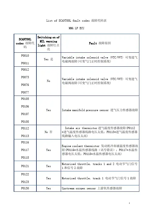
List of SCANTOOL fault codes 故障代码表MM6.LP ECUSCANTOOL codes 故障代码 Switching on ofMIL warninglight 故障灯点亮Fault 故障原因P0010P0011 Yes 是Variable intake solenoid valve (VTC/VVT) 可变进气电磁阀故障(可变气门正时控制系统)P0012 P0075P0076 P0077 NoVariable intake solenoid valve (VTC/VVT) 可变进气电磁阀故障(可变气门正时控制系统)P0105P0106P0107P0108Yes Intake manifold pressure sensor 进气压力传感器故障P0112P0113 No 否Intake air thermistor进气温度传感器故障(P0112=进气温度传感器线路电压太低;P0113=进气温度传感器线路输入电压太高)P0116P0117 P0118 YesEngine coolant thermistor 发动机冷却液温度传感器故障(P0116=水温传感器线路(讯号错误);P0117=水温传感器电压太低;P0118=水温传感器电压太高)P0121 Yes Motorised throttle, tracks 1 and 2 电动节气门信号1和信号2故障P0122P0123Yes Motorised throttle, track 1 电动节气门信号1故障 P0130 Yes Upstream oxygen sensor 上游氧传感器故障SCANTOOL codes 故障代码MIL warninglight 故障灯点亮Fault 故障原因P0131传感器线路电压太低或短路P0132氧传感器线路电压太高P0133 Yes Ageing of upstream oxygen sensor上游氧传感器老化P0135 Yes Upstream oxygen sensor heater control上游氧传感器加热控制故障(氧传感器的加热线路不良)P0136P0137 P0138 YesDownstream oxygen sensor 下游氧传感器故障(P0136=氧传感器失效;P0137=氧传感器线路短路;;P0138=氧传感器电压太高)P0141 Yes Downstream oxygen sensor heater control上游氧传感器加热控制故障(氧传感器的加热线路不良)P0170 Yes Fuel injection 燃油喷射故障(燃料修正(混合比)不良) P0201P0261 P0262 YesInjector 1 control 1缸喷油觜控制故障(P0201=第1缸喷油觜控制线路失效;P0261=第1缸喷油觜线路电压太低;P0262=第1缸喷油觜线路电压太高)P0202P0264 P0265 YesInjector 2 control 2缸喷油觜控制故障(P0202=第2缸喷油觜控制线路失效;P0264=第2缸喷油觜线路电压太低;P0265=第2缸喷油觜线路电压太高)P0203P0267 P0268 YesInjector 3 control3缸喷油觜控制故障(P0203=第3缸喷油觜控制线路失效;P0267=第3缸喷油觜线路电压太低;P0268=第3缸喷油觜线路电压太高)P0204 Yes Injector 4 control 4缸喷油觜控制故障(P0204=第4缸SCANTOOL codes 故障代码MIL warninglight 故障灯点亮Fault 故障原因P0269 P0270 喷油觜控制线路失效;P0269=第3缸喷油觜线路电压太低;P0270=第3缸喷油觜线路电压太高)P0221 Yes Accelerator pedal sensor, incoherence tracks 1 and 2 油门路板传感器1和2不一致.P0222P0223 YesAccelerator pedal sensor, track 1 油门踏板传感器信号1电压故障(P0222=电压太低;P0223=电压太高)P0227P0228 YesAccelerator pedal sensor, track 2油门踏板传感器信号2电压故障(P0227=电压太低;P0228=电压太高)P0300P1336 YesMisfiring on several cylinders or non-specificcylinder 某缸缺火或缺火缸情况不明确故障(P0330=引擎曾经有失火(MISFIRE)现象)P0301P1337Yes Cylinder 1 misfiring 1缸缺火 P0302P1338Yes Cylinder 2 misfiring 2缸缺火 P0303P1339Yes Cylinder 3 misfiring 3缸缺火 P0304P1340Yes Cylinder 4 misfiring 4缸缺火 P0335P0336 P0339 YesEngine speed sensor 发动机转速传感器故障(P0335=曲轴传感器A组线路失效;P0336=曲轴传器A电压值不正确;P0339=曲轴传器A组线路间歇故障)P0341 No Cylinder 1 reference sensor 1缸位置传感器故障(凸轮轴传感器线路电压值不正确)SCANTOOL codes 故障代码MIL warninglight 故障灯点亮Fault 故障原因P0351 Yes Ignition coil 1 control (1/4 if twin-static) 点火线圈控制故障(点火线圈1组一次/二次线路失效)P0352 Yes Ignition coil 2 control (2/3 if twin-static) 点火线圈控制故障(点火线圈2组一次/二次线路失效)P0353 Yes Ignition coil 3 control点火线圈控制故障(点火线圈3组一次/二次线路失效)P0354 Yes Ignition coil 4 control点火线圈控制(点火线圈4组一次/二次线路失效)P0400P0401 P0402 YesExhaust gases recirculation 废气再循环故障(P0400=EGR阀系统流量控制失效;P0401=EGR阀系统流量控制不正确或太低(阻塞)引擎达工作温度,车速80KM以上行驶3~5分钟但EGR温度信号低于40℃;P0402=EGR阀系统流量控制太大(泄漏))P0403 No Exhaust gases recirculation废气再循环故障(EGR阀流量电磁阀控制线路不良)P0404P1456 NoEGR solenoid valve learning EGR电磁阀学习故障(P0404=EGR阀流量电磁阀控制线路电压值不正确)P0405P0406 NoEGR valve position sensor EGR阀位置传感器故障(P0405=EGR阀流量传感器线路A组电压太低;P0406 =EGR阀流量传感器线路A组电压太高)P0410 Yes Air injection at exhaust二次空气注入故障(二次空气导入系统失效)P0413P0414 YesAir pump空气泵故障(P0413=二次空气导入系统流量电磁阀A组线路断路;P0414=二次空气导入系统流量电磁阀A组线路短路P0420 Yes Ageing of catalytic converter催化转换器老化(触媒系统净化效能太低)P0444P0445 YesPurge canister solenoid valve 碳罐电磁阀故障(P0444=燃油蒸发控制系统碳罐电磁伐控制线路断路或电压太低;P0445=燃油蒸发控制系统碳罐电磁伐控制线路断路或电压太高)SCANTOOL codes 故障代码MIL warninglight 故障灯点亮Fault 故障原因P0461P0462 P0463 NoFuel gauge 燃油表故障(P0461=燃油油面高度传器线路电压值不正确;P0462=燃油高度传器线路电压太低;P0463=燃油高度传器线路电压太高)P0500 Yes Vehicle speed sensor 车速传感器故障(车速传器线路失效或间歇不良)P0562P0563 YesBattery voltage 电瓶电压故障(P0562=电瓶电压太低;P0563=电瓶电压太高)P0571 No Incoherence between the two stop switches双功能刹车开关不一致(定速控制系统刹车开关线路A组失效)P0606 Yes Injection ECU 喷射ECU(ECM电脑失效) P0608P0609Yes Sensors supply 供给系统传感器故障P1133 Yes Motorised throttle track 1/ Pressure incoherence 节气门开度信号1/进气压力不一致P1134 Yes Motorised throttle track 2/ Pressure incoherence 节气门开度信号2/进气压力不一致P1152 Yes ECU ECU故障P1153 Yes Throttle stops learning 节气门止点学习故障P1157P1158Yes Motorised throttle, track 2节气门传感器信号2 故障P1160 Yes Intake air pipe leak 进气管漏气故障P1161 Yes Throttle position control 节气门位置控制故障P1290P1292 P1293 NoBi-mode solenoid valve (variable air intake) 双模式电磁阀故障(可变进气系统)SCANTOOL codes 故障代码MIL warninglight 故障灯点亮Fault 故障原因P1613 Yes Configuration 配置故障P1617 Yes ECU ECU故障P1621P1622P1623P1624P1625P1626P1627P1628P1629P1630Yes Safety faults 安全故障P1631 Yes ECU ECU故障P2100P2101P2102P2103Yes Motorised throttle ECU 节气门体(模块)故障P2143P2144P2145Yes EGR valve EGR阀故障U0028 Yes Comfort Van network fault VAN网(舒适网)故障 U0037 Yes Body van network fault VAN(车身网)网故障SCANTOOL codes 故障代码MIL warninglight 故障灯点亮Fault 故障原因U0103U0404 YesDialogue with the automatic gearbox 与自动变速箱通话故障U0121U0415Yes Dialogue with the ABS or ESP 与ABS或ESP通话故障U1000 Yes The ECU is no longer communicating on the network 该ECU与网络无长久通信U1003 Yes No communication on the CAN network不与CAN网通信U1118U1218Yes Dialogue with the BSI 与BSI通话故障武汉宝狮技术室17/04/2006。
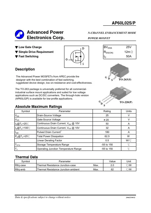
N-CHANNEL ENHANCEMENT MODE POWER MOSFETAbsolute Maximum RatingsSymbol Units V DS V V GSV I D @T C =25℃A I D @T C =100℃A I DMA P D @T C =25℃W W/℃T STG ℃T J℃Symbol Value Unit Rthj-case Thermal Resistance Junction-case Max. 2.0℃/W Rthj-ambThermal Resistance Junction-ambientMax.62℃/WData & specifications subject to change without notice200218032Thermal DataParameterPulsed Drain Current 1180Operating Junction Temperature Range-55 to 150Linear Derating Factor 0.5Storage Temperature RangeTotal Power Dissipation 62.5-55 to 150Continuous Drain Current, V GS @ 10V 50Continuous Drain Current, V GS @ 10V 32Drain-Source Voltage 25Gate-Source VoltageAP60L02S/PParameterRating ± 20G DSTO-263(S)GDS TO-220(P)Electrical Characteristics@T j =25o C(unless otherwise specified)Symbol ParameterTest ConditionsMin.Typ.Max.Units BV DSSDrain-Source Breakdown VoltageV GS =0V, I D =250uA 25--V ΔB V DSS /ΔT jBreakdown Voltage Temperature Coefficient Reference to 25℃, I D =1mA-0.037-V/℃R DS(ON)Static Drain-Source On-Resistance V GS =10V, I D =25A --12m ΩV GS =4.5V, I D =20A --26m ΩV GS(th)Gate Threshold Voltage V DS =V GS , I D =250uA 1-3V g fs Forward TransconductanceV DS =10V, I D =25A -30-S I DSS Drain-Source Leakage Current (T j =25o C)V DS =25V, V GS =0V --1uA Drain-Source Leakage Current (T j =150o C)V DS =20V, V GS =0V --25uA I GSS Gate-Source Leakage V GS =--nA Q g Total Gate Charge 2I D =25A -21nC Q gs Gate-Source Charge V DS =20V - 2.8nC Q gd Gate-Drain ("Miller") Charge V GS =5V -16nC t d(on)Turn-on Delay Time 2V DS =15V -8-ns t r Rise TimeI D =20A-75-ns t d(off)Turn-off Delay Time R G =3.3Ω,V GS =10V -22-ns t f Fall Time R D =0.75Ω-20-ns C iss Input Capacitance V GS =0V -605-pF C oss Output CapacitanceV DS =25V -415-pF C rssReverse Transfer Capacitancef=1.0MHz-195-pFSource-Drain DiodeSymbol ParameterTest ConditionsMin.Typ.Max.Units I S Continuous Source Current ( Body Diode )V D =V G =0V , V S =1.26V --50A I SM Pulsed Source Current ( Body Diode )1--180A V SDForward On Voltage 2T j =25℃, I S =50A, V GS =0V--1.26VNotes:1.Pulse width limited by safe operating area.2.Pulse width <300us , duty cycle <2%.AP60L02S/P±100± 20VAP60L02S/PFig 1. Typical Output Characteristics Fig 2. Typical Output CharacteristicsFig 3. On-Resistance v.s. Gate VoltageFig 4. Normalized On-Resistancev.s. Junction TemperatureAP60L02S/PFig 5. Maximum Drain Current v.s. Fig 6. Typical Power DissipationCase TemperatureFig 7. Maximum Safe Operating AreaFig 8. Effective Transient Thermal ImpedanceAP60L02S/PFig 9. Gate Charge Characteristics Fig 10. Typical Capacitance CharacteristicsReverse DiodeJunction TemperatureAP60L02S/PFig 13. Switching Time Circuit Fig 14. Switching Time WaveformFig 15. Gate Charge Circuit Fig 16. Gate Charge Waveform。
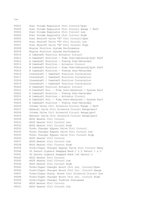
IsoP0001Fuel Volume Regulator Ctrl Circuit/OpenP0002Fuel Volume Regulator Ctrl Circuit Range / PerfP0003Fuel Volume Regulator Ctrl Circuit LowP0004Fuel Volume Regulator Ctrl Circuit HighP0005Fuel Shutoff Valve "A" Ctrl Circuit/OpenP0006Fuel Shutoff Valve "A" Ctrl Circuit LowP0007Fuel Shutoff Valve "A" Ctrl Circuit HighP0008Engine Position System PerformanceP0009Engine Position System PerformanceP0010 A Camshaft Position Actuator CircuitP0011 A Camshaft Position - Time Over-Advanced/Syst Perf P0012 A Camshaft Position - Timing Over-RetardedP0013 B Camshaft Position - Actuator CircuitP0014 B Camshaft Position - Time Over-Advanced/Syst Perf P0015 B Camshaft Position - Timing Over-RetardedP0016Crankshaft / Camshaft Position CorrelationP0017Crankshaft / Camshaft Position CorrelationP0018Crankshaft / Camshaft Position CorrelationP0019Crankshaft / Camshaft Position CorrelationP0020 A Camshaft Position Actuator CircuitP0021 A Camshaft Pos. - Time Over-Advanced / System Perf P0022 A Camshaft Position - Timing Over-RetardedP0023 B Camshaft Position - Actuator CircuitP0024 B Camshaft Pos. - Time Over-Advanced / System Perf P0025 B Camshaft Position - Timing Over-RetardedP0026Intake Valve Ctrl Solenoid Circuit Range / PerfP0027Exhaust Valve Ctrl Solenoid Circuit Range/perfP0028Intake Valve Ctrl Solenoid Circuit Range/perfP0029Exhaust Valve Ctrl Solenoid Circuit Range/perfP0030HO2S Heater Ctrl CircuitP0031HO2S Heater Ctrl Circuit LowP0032HO2S Heater Ctrl Circuit HighP0033Turbo Charger Bypass Valve Ctrl CircuitP0034Turbo Charger Bypass Valve Ctrl Circuit LowP0035Turbo Charger Bypass Valve Ctrl Circuit HighP0036HO2S Heater Ctrl CircuitP0037HO2S Heater Ctrl Circuit LowP0038HO2S Heater Ctrl Circuit HighP0039Turbo/Super Charger Bypass Valve Ctrl Circuit Rang P0040O2 Sensor Signals Swapped Bank 1 & 2 Sensor 1 & 2 P0041O2 Sensor Signals Swapped Bank 1&2 Sensor 2P0042HO2S Heater Ctrl CircuitP0043HO2S Heater Ctrl Circuit LowP0044HO2S Heater Ctrl Circuit HighP0045Turbo/Super Charger Boost Ctrl Sol. Circuit/OpenP0046Turbo/Super Charger Boost Ctrl Sol. Circuit Range P0047Turbo/Super Charg. Boost Ctrl Solenoid Circuit Low P0048Turbo/Super Charger Boost Ctrl Sol. Circuit HighP0049Turbo/Super Charger Turbine OverspeedP0050HO2S Heater Ctrl CircuitP0051HO2S Heater Ctrl Circuit LowP0052HO2S Heater Ctrl Circuit HighP0053HO2S Heater ResistanceP0054HO2S Heater ResistanceP0055HO2S Heater ResistanceP0056HO2S Heater Ctrl CircuitP0057HO2S Heater Ctrl Circuit LowP0058HO2S Heater Ctrl Circuit HighP0059HO2S Heater ResistanceP0060HO2S Heater ResistanceP0061HO2S Heater ResistanceP0062HO2S Heater Ctrl CircuitP0063HO2S Heater Ctrl Circuit LowP0064HO2S Heater Ctrl Circuit HighP0065Air Assisted Injector Ctrl Range/PerformanceP0066Air Assisted Injector Ctrl Circuit or Circuit Low P0067Air Assisted Injector Ctrl Circuit HighP0068MAP/MAF - Throttle Position CorrelationP0069Manifold Absolute / Barometric Press. Correlation P0070Ambient Air Temperature Sensor CircuitP0071Ambient Air Temperature Sensor Range/PerformanceP0072Ambient Air Temperature Sensor Circuit LowP0073Ambient Air Temperature Sensor Circuit HighP0074Ambient Air temp Sensor Circuit IntermittentP0075Intake Valve Ctrl Solenoid CircuitP0076Intake Valve Ctrl Solenoid Circuit LowP0077Intake Valve Ctrl Solenoid Circuit HighP0078Exhaust Valve Ctrl Solenoid CircuitP0079Exhaust Valve Ctrl Solenoid Circuit LowP0080Exhaust Valve Ctrl Solenoid Circuit HighP0081Intake Valve Ctrl Solenoid CircuitP0082Intake Valve Ctrl Solenoid Circuit LowP0083Intake Valve Ctrl Solenoid Circuit HighP0084Exhaust Valve Ctrl Solenoid CircuitP0085Exhaust Valve Ctrl Solenoid Circuit LowP0086Exhaust Valve Ctrl Solenoid Circuit HighP0087Fuel Rail/System Pressure - Too LowP0088Fuel Rail/System Pressure - Too HighP0089Fuel Pressure Regulator 1 PerformanceP0090Fuel Pressure Regulator 1 Ctrl CircuitP0091Fuel Pressure Regulator 1 Ctrl Circuit LowP0092Fuel Pressure Regulator 1 Ctrl Circuit HighP0093Fuel System Leak Detected - Large LeakP0094Fuel System Leak Detected - Small LeakP0095Intake Air Temperature Sensor 2 CircuitP0096Intake Air Temperature Sensor 2 Circuit Range/perf P0097Intake Air Temperature Sensor 2 Circuit LowP0098Intake Air Temperature Sensor 2 Circuit HighP0099Intake Air temp Sensor 2 Circuit Interm. / Erratic P0100Masse ou volume d’air : dysfonctionnement circuit P0101Volume air : pb domaine fct. /perf circuitP0102Masse ou volume d air : circuit, entree basseP0103Masse ou volume d air : circuit, entree hauteP0104Masse ou volume d air : circuit intermittentP0105press. absolue tubulure admis. / barom. : dysfct. P0106press. barometrique : pb. domaine fonct.P0107press. barometrique : circuit, entree basseP0108press. barometrique : circuit, entree hauteP0109press. barometrique : circuit intermittentP0110temp. de l’air d’admission : dysfct. circuitP0111Temp air admission : pb domaine fct. /perf circuit P0112Temp de l air d admission : circuit, entree basse P0113Temp de l air d admission : circuit, entree haute P0114Temp de l air d admission : circuit intermittentP0115Temp liquide refroidissement : dysfonct. circuitP0116Temp liquide refroidissement : pb domaine fctP0117Temp liquide refroidissement : entree basseP0118temp. liquide refroidissement : entree hauteP0119temp. liquide refroidissement : circuit interm.P0120Papillon /capt pos. pedale /Com. A: dysfct circuit P0121Papillon /capt pos. pedale /Com. A: pb domaine fct P0122Papillon /capt pos. pedale /Com. A: entree basseP0123Papillon /capt pos. pedale /Com. A: entree hauteP0124Papillon /capt pos. pedale/Com. A: circuit interm. P0125Temp liquide refroid. insuff pour Ctrl carbuP0126Temp liquide refroid. insuff pour fct. stableP0127Intake Air Temperature Too HighP0128Coolant Therm. ( temp Below Therm. Regul temp)P0129Barometric Pressure Too LowP0130Sonde O2 : mauvais fonct. (rangee 1, sonde 1)P0131Sonde O2 : tension basse (Rangee 1 Sonde 1)P0132Sonde O2 : tension haute (Rangee 1 Sonde 1)P0133Sonde O2 : circuit, rep. lente (Rangee 1 Sonde 1) P0134Sonde O2 : pas activite (Rangee 1 Sonde 1)P0135Chauff sonde O2 : dysfct. circuit (Rang 1 Sonde 1) P0136Sonde O2 : mauvais fonct. (rangee 1, sonde 2)P0137Sonde O2 : tension basse (Rangee 1 Sonde 2)P0138Sonde O2 : tension haute (Rangee 1 Sonde 2)P0139Sonde O2 : circuit, rep. lente (Rangee 1 Sonde 2) P0140Sonde O2 : pas activite (Rangee 1 Sonde 2)P0141Chauff sonde O2 : dysfct. circuit (Rang 1 Sonde 2) P0142Sonde O2 : mauvais fonct. (rangee 1, sonde 3)P0143Sonde O2 : tension basse (Rangee 1 Sonde 3)P0144Sonde O2 : tension haute (Rangee 1 Sonde 3)P0145Sonde O2 : circuit, rep. lente (Rangee 1 Sonde 3) P0146Sonde O2 : pas activite (Rangee 1 Sonde 3)P0147Chauff sonde O2 : dysfct. circuit (Rang 1 Sonde 3) P0148Fuel Delivery ErrorP0149Fuel Timing ErrorP0150Sonde O2 : mauvais fonct. (rangee 2, sonde 1)P0151Sonde O2 : tension basse (Rangee 2 Sonde 1)P0152Sonde O2 : tension haute (Rangee 2 Sonde 1)P0153Sonde O2 : circuit, rep. lente (Rangee 2 Sonde 1) P0154Sonde O2 : pas activite (Rangee 2 Sonde 1)P0155Chauff sonde O2 : dysfct. circuit (Rang 2 Sonde 1) P0156Sonde O2 : mauvais fonct. (rangee 2, sonde 2)P0157Sonde O2 : tension basse (Rangee 2 Sonde 2)P0158Sonde O2 : tension haute (Rangee 2 Sonde 2)P0159Sonde O2 : circuit, rep. lente (Rangee 2 Sonde 2) P0160Sonde O2 : pas activite (Rangee 2 Sonde 2)P0161Chauff sonde O2 : dysfct. circuit (Rang 2 Sonde 2) P0162Sonde O2 : mauvais fonct. (rangee 2, sonde 3)P0163Sonde O2 : tension basse (Rangee 2 Sonde 3)P0164Sonde O2 : tension haute (Rangee 2 Sonde 3)P0165Sonde O2 : circuit, rep. lente (Rangee 2 Sonde 3) P0166Sonde O2 : pas activite (Rangee 2 Sonde 3)P0167Chauff sonde O2 : dysfct. circuit (Rang 2 Sonde 3) P0168Fuel Temperature Too HighP0169Incorrect Fuel CompositionP0170Def fct. / panne systeme injection carbu (regul 1) P0171Systeme trop pauvre (Rangee 1)P0172Systeme trop riche (Rangee 1)P0173Def fct. / panne systeme injection carbu (regul 2) P0174Systeme trop pauvre (Rangee 2)P0175Systeme trop riche (Rangee 2)P0176Composition du carburant, capt : dysfonct. circuit P0177Capt compos. carburant : circuit, domaine fonct.P0178Capt compos. carburant : circuit, entree basseP0179Capt compos. carburant : circuit, entree hauteP0180Capt de temp carburant A : circuit, dysfonct.P0181Capt temp carburant A : circuit, domaine fonct.P0182Capt de temp carburant A : circuit, entree basseP0183Capt de temp carburant A : circuit, entree hauteP0184Capt de temp carburant A : circuit intermittentP0185Capt de temp carburant B : circuit, dysfonct.P0186capt temp carburant B : circuit, domaine fonct.P0187Capt de temp carburant B : circuit, entree basseP0188Capt de temp carburant B : circuit, entree hauteP0189Capt de temp carburant B : circuit intermittentP0190Capt. de press. rampe d’inject. : circuit, dysfct. P0191Capt press. rampe injection : domaine fonct.P0192Capt press. rampe injection : entree basseP0193Capt press. rampe injection : entree hauteP0194Capt press. rampe injection : circuit intermittent P0195Capteur de temperature huile moteur : dysfonct.P0196capt temp huile moteur : domaine fonct. / perfP0197Capteur de temperature huile moteur : panne basse P0198Capteur de temperature huile moteur : panne haute P0199Capteur de temperature huile moteur : intermittent P1004Signal de guidage VVT : Entree basseP1005Signal de guidage VVT : dysfonctionnement circuit P1006Signal de guidage VVT : Entree hauteP1007Signal de guidage VVT : domaine de fct. / perf.P1011Signal de reference VVT : Entree basseP1012Signal de reference VVT : dysfonct. circuitP1013Signal de reference VVT : Entree hauteP1014Signal de reference VVT : domaine de fct. / perf. P1017Signal reference / guidage VVT : dom fct. / perf. P101A Apprentissage VVT : dysfonctionnement circuitP101C Moteur VVT : panne basseP101D Moteur VVT : dysfonctionnement circuitP101E Moteur VVT : domaine de fct. / performanceP1023Ecart butees apprentissages moteur VVT : trop haut P1024Butee basse apprent. moteur VVT: dysfonct. circuit P1025Butees apprentissages moteur VVT : dom fct./ perf. P1031Signal angle recopie moteur VVT : dom fct. / perf. P1064Position init moteur VVT : dysfonct. circuitP1077Temperature moteur VVT : trop hauteP1078Temp. etage puissance moteur VVT : trop hauteP1100Parametre d adapt. pos. vanne EGR (adapt off egr) P1101capt de pression atmospherique : dysfonct. circuit P1102Capt. de levee d’aiguille : dysfct. circuitP1103Capteur position coulisseau : dysfonct. circuitP1104Electrovanne aerovariable : dysfonct. circuitP1105Electrovanne injecteur ventile : dysfonct. circuit P1106Electrovanne avance (regul avance) : dysfct.P1107Commande swirl variableP1108Param adapt. qte air collecteur (adapt bias tot)P1109Param adapt. qte air collecteur (adapt lin1 thro) P110A Mass or Volume Air Flow "B" CircuitP110B Mass or Volume Air Flow "B" Circuit Range/Perf.P110C Mass or Volume Air Flow "B" Circuit Low InputP110E Mass or Volume Air Flow B Circuit Interm./Erratic P110F Mass or Volume Air Flow Sensor A/B CorrelationP1110Param adapt. qte air collecteur (adapt lin2 thro) P1111Param adapt. pos. vanne EGR (adapt gain egr)P1112Regulation debitP1113Pression rail trop faibleP1114Fonctionnalite arret moteur : arret par injection P1115Sonde O2 : gain, pb de dom. de fct. / perf.P1116Sonde O2 : offset, pb de dom. de fct. / perf.P1117Capt press. atmospherique : circuit, entree basse P1118Capt press. atmospherique : circuit, entree haute P1119Capt press. atmospherique : circuit intermittentP1120Capt. de levee d’aiguille : circuit, entree basse P1121Capt. de levee d’aiguille : circuit, entree haute P1122Capteur de levee d’aiguille : circuit intermittent P1123Capt position coulisseau : circuit, entree basseP1124Capt position coulisseau : circuit, entree hauteP1125Capteur position coulisseau : circuit intermittent P1126Electrovanne aerovariable : circuit ouvertP1127Electrovanne aerovariable : court-circuitP1128Electrovanne injecteur ventile : circuit ouvertP1129Electrovanne injecteur ventile : court-circuitP1130Electrovanne avance (regul avance): circuit ouvert P1131Electrovanne avance (regul avance): court-circuit P1132Sonde AT1 et sonde AT2 en defautP1133Incoherence papillon 1 / PressionP1134Incoherence papillon 2 / PressionP1135Actionneur desactivation debit : dysfonct. circuit P1136Actionneur desactivation de debit : circuit ouvert P1137Actionneur desactivation de debit : court-circuit P1138Actionneur limiteur press. carbu : dysfct. circuitP1139Actionneur limiteur press. carbu : circuit ouvert P1140Actionneur limiteur press. carbu : court-circuitP1141Capt de temperature catalyseur : dysfonct. circuit P1142Capteur de temperature catalyseur : entree basseP1143Capteur de temperature catalyseur : entree hauteP1144Capt de temp catalyseur : circuit intermittentP1145Bruit sur levee d’aiguilleP1146Contrôle levee d’aiguilleP1147Electrov dephas arbre a came (VTC1/VVT1): dom fct. P1148Electrov dephaseur arbre a cames (VTC1/VVT1) : CO P1149Electrov dephaseur arbre a cames (VTC1/VVT1) : CC P1150Commande papillon : circuit ouvertP1151Commande papillon : cort-circuit au plusP1152Moteur papillon : dysfonctionnement driverP1153Apprentissage butees papillonP1154Commande papillon : court-circuit a la masseP1155Masse d’essence non brule trop importanteP1156Capt. d’angle papillon 2 : dysfct. circuitP1157Capteur d’angle papillon 2 : entree basseP1158Capteur d’angle papillon 2 : entree hauteP1159Capteur d’angle papillon 2 : circuit intermittent P2177Tubulure d’admission : fuite detecteeP1161Contrôleur de position papillon : pb de perf.P1162Contrôleur de position de vanne EGR : pb de perf. P1163Faute absence de recalage accelerometreP1164Offset pression railP1165Differentiel de pression trop basP1166Pression rail trop forteP1167Surveillance dynamique de la pressionP1168Courant regulateur press. : domaine fonct.P1169Tension booster n°1P1170Tension booster n°2P1171Post FonctionnementP1172Electrov dephas arbre a came (VTC2/VVT2): dom fct. P1173Electrov dephaseur arbre a cames (VTC2/VVT2) : CO P1174Electrov dephaseur arbre a cames (VTC2/VVT2) : CC P1175Electrovanne VCV : dysfonctionnement circuitP1176Electrov. VCV : dom. de fct. / perf.P1177Electrovanne VCV : panne basseP1179Electrovanne VCV : panne hauteP1180Electrovanne VCV : circuit intermittentP1181Pression Isovac : dysfonctionnement circuitP1182press. Isovac : pb dom. de fct. / perf.P1183Pression Isovac : circuit, entree basseP1184Pression Isovac : circuit, entree hauteP1185Pression Isovac : circuit intermittentP1186Def fct. / panne systeme injection carbu (regul 1) P1187Systeme trop pauvre (Rangee 1)P1188Systeme trop riche (Rangee 1)P1189Def fct. / panne systeme injection carbu (regul 2) P1190Systeme trop pauvre (Rangee 2)P1191Systeme trop riche (Rangee 2)P1192Fct arret moteur : arret par systeme press. railP1193Injecteur 1 : defaut mecaniqueP1194Injecteur 2 : defaut mecaniqueP1195Injecteur 3 : defaut mecaniqueP1196Injecteur 4 : defaut mecaniqueP1197Defaillance globale au niveau injecteur / faisceau P1198Defaut adaptation en butee sur regulateur VCVP1199Strategie anti-desamorcage activeP119A Defauts detectes en niveau mini-carburantP119B Erreur classification injecteur 1: pb code ISA/IMA P119C Erreur classification injecteur 2: pb code ISA/IMA P119D Erreur classification injecteur 3: pb code ISA/IMA P119E Erreur classification injecteur 4: pb code ISA/IMA P119F Défaut dilution d’huileP11A0Stratégie FMA : Correction maxiP11A1Stratégie FMA : Correction miniP11A2Stratégie FMA : Correction non plausibleP0200Injecteur : dysfonctionnement circuitP0201Cylindre 1 - Injecteur : dysfonctionnement circuit P0202Cylindre 2 - Injecteur : dysfonctionnement circuit P0203Cylindre 3 - Injecteur : dysfonctionnement circuit P0204Cylindre 4 - Injecteur : dysfonctionnement circuit P0205Cylindre 5 - Injecteur : dysfonctionnement circuit P0206Cylindre 6 - Injecteur : dysfonctionnement circuit P0207Cylindre 7 - Injecteur : dysfonctionnement circuit P0208Cylindre 8 - Injecteur : dysfonctionnement circuit P0209Cylindre 9 - Injecteur : dysfonctionnement circuit P0210cyl. 10 - Injecteur : dysfct. circuitP0211cyl. 11 - Injecteur : dysfct. circuitP0212cyl. 12 - Injecteur : dysfct. circuitP0213Injecteur 1 de demarrage a froid : dysfonct.P0214Injecteur 2 de demarrage a froid : dysfonct.P0215Relais principal : dysfonctionnementP0217Surtemperature moteurP0218Surtemperature transmissionP0219Surregime moteurP0220Papillons gaz / capt pos. pedale / Com. B : dysfct P0221Pap. gaz/ capt pos. Ped/ Commut. B: pb domaine fct P0222Pap. gaz/ capt pos. pedale / Com. B : entree basse P0223Pap. gaz/ capt pos. pedale / Com. B : entree haute P0224Pap. gaz / capt pos. pedale / Com. B : intermit.P0225Papillons gaz / capt pos. pedale / Com. C : dysfct P0226Pap. gaz/ capt pos. Ped/ Commut. C: pb domaine fct P0227Pap. gaz/ capt pos. pedale / Com. C : entree basse P0228Pap. gaz/ capt pos. pedale / Com. C : entree haute P0229Pap. gaz / capt pos. pedale / Com. C : intermit.P0230Pompe a carburant, circuit primaire : dysfonct.P0231Pompe a carburant circuit secondaire : panne basse P0232Pompe a carburant circuit secondaire : panne haute P0233Pompe carburant, circuit secondaire : intermittent P0234Engine overboost conditionP0235Capteur de turbocompresseur A : dysfonct. circuit P0236Capt turbocompresseur A : circuit, domaine fonct. P0237Capt de turbocompresseur A : circuit, panne basseP0238Capt de turbocompresseur A : circuit, panne haute P0239Capteur de turbocompresseur B : dysfonct. circuit P023D Manifold Press Turbo/Supercharger Boost Cpt A Corr P023E Manifold Press Turbo/Supercharger Boost Cpt B Corr P0240Capt turbocompresseur B : circuit, domaine fonct. P0241Capt de turbocompresseur B : circuit, panne basse P0242Capt de turbocompresseur B : circuit, panne haute P0243Relais A soupape decharge turbocompress : dysfct. P0244Relais A soupape decharge turbocompress : dom fct. P0245Relais A soupape decharge turbocomp : panne basse P0246Relais A soupape decharge turbocomp : panne haute P0247Relais B soupape decharge turbocompress : dysfct. P0248Relais B soupape decharge turbocompress : dom fct. P0249Relais B soupape decharge turbocomp : panne basse P0250Relais B soupape decharge turbocomp : panne haute P0251Rotor / Came de la pompe d’injection A : dysfct.P0252Rotor / Came la pompe injection A : domaine fct.P0253Rotor / Came la pompe injection A : panne basseP0254Rotor / Came la pompe injection A : panne hauteP0255Rotor / Came la pompe injection A : intermittentP0256Rotor / Came de la pompe d’injection B : dysfct.P0257Rotor / Came la pompe injection B : domaine fct.P0258Rotor / Came la pompe injection B : panne basseP0259Rotor / Came la pompe injection B : panne hauteP0260Rotor / Came la pompe injection B : intermittentP0261Injecteur cylindre 1 : circuit, panne basseP0262Injecteur cylindre 1 : circuit, panne hauteP0263Cyl. 1 : defaillance niv contribution / equilibre P0264Injecteur cylindre 2 : circuit, panne basseP0265Injecteur cylindre 2 : circuit, panne hauteP0266Cyl. 2 : defaillance niv contribution / equilibre P0267Injecteur cylindre 3 : circuit, panne basseP0268Injecteur cylindre 3 : circuit, panne hauteP0269Cyl. 3 : defaillance niv contribution / equilibre P0270Injecteur cylindre 4 : circuit, panne basseP0271Injecteur cylindre 4 : circuit, panne hauteP0272Cyl. 4 : defaillance niv contribution / equilibre P0273Injecteur cylindre 5 : circuit, panne basseP0274Injecteur cylindre 5 : circuit, panne hauteP0275Cyl. 5 : defaillance niv contribution / equilibre P0276Injecteur cylindre 6 : circuit, panne basseP0277Injecteur cylindre 6 : circuit, panne hauteP0278Cyl. 6 : defaillance niv contribution / equilibre P0279Injecteur cylindre 7 : circuit, panne basseP0280Injecteur cylindre 7 : circuit, panne hauteP0281Cyl. 7 : defaillance niv contribution / equilibre P0282Injecteur cylindre 8 : circuit, panne basseP0283Injecteur cylindre 8 : circuit, panne hauteP0284Cyl. 8 : defaillance niv contribution / equilibre P0285Injecteur cylindre 9 : circuit, panne basseP0286Injecteur cylindre 9 : circuit, panne hauteP0287Cyl. 9 : defaillance niv contribution / equilibre P0288Injecteur cylindre 10 : circuit, panne basseP0289Injecteur cylindre 10 : circuit, panne hauteP0290Cyl. 10 : defaillance niv contribution / equilibre P0291Injecteur cylindre 11 : circuit, panne basseP0292Injecteur cylindre 11 : circuit, panne hauteP0293Cyl. 11 : defaillance niv contribution / equilibre P0294Injecteur cylindre 12 : circuit, panne basseP0295Injecteur cylindre 12 : circuit, panne hauteP0296Cyl. 12 : defaillance niv contribution / equilibre P0297Vehicle Overspeed ConditionP0298Engine Oil Over TemperatureP0299Turbo/Super Charger UnderboostP1200Capteur pression FSS : dysfonctionnement circuitP1201Capteur pression FSS : domaine de fonct. /perfP1202Capteur pression FSS : circuit, entree basseP1203Capteur pression FSS : circuit, entree hauteP1204Capteur pression FSS : circuit intermittentP1205regul. d’avance : dom. de fct. / perf.P1206Electrovanne regul press. carbu : dysfct. circuit P1207Electrovanne regul press. carbu : domaine fct.P1208Electrov. regul. press. carburant : panne basseP1209Electrov. regul. press. carburant : panne hauteP1210Electrov. regul. press. carburant : COP1211Commutateur (GPL)P1212Electrovanne reservoir : dysfonctionnement circuit P1213Electrovanne reservoir : domaine de fonct. / perf P1214Electrovanne reservoir : circuit, panne basseP1215Electrovanne reservoir : circuit, panne hauteP1216Electrovanne reservoir : circuit intermittentP1217Electrovanne GPL : dysfonctionnement circuitP1218Electrovanne GPL : domaine de fonct. / perfP1219Electrovanne GPL : circuit, panne basseP1220Electrovanne GPL : circuit, panne hauteP1221Electrovanne GPL : circuit intermittentP1222Distributeur SMART (PWM1) : dysfonct. circuitP1223Distributeur SMART (PWM1) : domaine fonct. / perf P1224Distributeur SMART (PWM1) : circuit, panne basseP1225Distributeur SMART (PWM1) : circuit, panne hauteP1226Distributeur SMART (PWM1) : circuit intermittentP1227Distributeur SMART (PWM2) : dysfonct. circuitP1228Distributeur SMART (PWM2) : domaine fonct. / perf P1229Distributeur SMART (PWM2) : circuit, panne basseP1230Distributeur SMART (PWM2) : circuit, panne hauteP1231Distributeur SMART (PWM2) : circuit intermittentP1232Distributeur SMART (PCM1) : dysfonct. circuitP1233Distributeur SMART (PCM1) : domaine fonct. / perf P1234Distributeur SMART (PCM1) : circuit, panne basseP1235Distributeur SMART (PCM1) : circuit, panne hauteP1236Distributeur SMART (PCM1) : circuit intermittentP1237Distributeur SMART (PCM2) : dysfonct. circuitP1238Distributeur SMART (PCM2) : domaine fonct. / perf P1239Distributeur SMART (PCM2) : circuit, panne basseP1240Distributeur SMART (PCM2) : circuit, panne hauteP1241Distributeur SMART (PCM2) : circuit intermittentP1242Distributeur SMART (PCM4) : dysfonct. circuitP1243Distributeur SMART (PCM4) : domaine fonct. / perf P1244Distributeur SMART (PCM4) : circuit, panne basseP1245Distributeur SMART (PCM4) : circuit, panne hauteP1246Distributeur SMART (PCM4) : circuit intermittentP1247Distributeur SMART (PCM8) : dysfonct. circuitP1248Distributeur SMART (PCM8) : domaine fonct. / perf P1249Distributeur SMART (PCM8) : circuit, panne basseP1250Distributeur SMART (PCM8) : circuit, panne hauteP1251Distributeur SMART (PCM8) : circuit intermittentP1252Distributeur SMART (General) : dysfonct. circuitP1253Distributeur SMART (General) : domaine fct. / perf P1254Distributeur SMART (General) : circuit panne basse P1255Distributeur SMART (General) : circuit panne haute P1256Distributeur SMART (General) : circuit interm.P1257Signal GPLP1258Signal regime moteur (pour le GPL)P1259Signal injecteur 1P1260Signal injecteur 2P1261Signal injecteur 3P1262Signal injecteur 4P1263Capteur pression P1 : dysfonctionnement circuitP1264Capteur pression P1 : domaine de fonct. / perfP1265Capteur pression P1 : circuit, entree basseP1266Capteur pression P1 : circuit entree hauteP1267Capteur pression P1 : circuit intermittentP1268Capteur pression P2 : dysfonctionnement circuitP1269Capteur pression P2 : domaine de fonct. / perfP1270Capteur pression P2 : circuit, entree basseP1271Capteur pression P2 : circuit, entree hauteP1272Capteur pression P2 : circuit intermittentP1273Signal M.A.PP1274Capteur de temperature GPL : dysfonct. circuitP1275Capt de temperature GPL : domaine de fonct. / perf P1276Capteur de temperature GPL : circuit, entree basse P1277Capteur de temperature GPL : circuit, entree haute P1278Capteur de temperature GPL : circuit intermittent P1279Signal temperature eau moteurP1280Signal position papillonP1281Alimentation capteurs de pressionP1282Pression gazP1283Electrovanne detendeur : dysfonctionnement circuit P1284Electrovanne detendeur : domaine de fonct. / perf P1285Electrovanne detendeur : circuit, panne basseP1286Electrovanne detendeur : circuit, panne hauteP1287Electrovanne detendeur : circuit intermittentP1288Pression rail carburant : valeur basse (seuil 1)P1289Bi-mode, activ. 2eme conduit adm d’air : dysfct.P1290Bi-mode, activ. 2eme conduit adm d’air : dom perf P1291Pression rail carburant : valeur basse (seuil 2)P1292Bi-mode, activ. 2eme conduit adm air : panne basse P1293Bi-mode, activ. 2eme conduit adm air : panne haute P1294Pression rail carburant : valeur haute (seuil 1)P1295Bi-mode, activ. 2eme conduit adm air : intermitP1296Injecteur additif : circuit ouvertP1297Pression rail carburant : valeur haute (seuil 2)P1298Injecteur additif : circuit, panne hauteP1299Injecteur additif : circuit, panne basseP129A Boucle VT2 : ecart positifP129B Boucle VT2 : ecart negatifP129C Apprentissage VT2 : ecart longP129D Apprentissage VT2 : ecart courtP129E Vanne VT2 : dysfonctionnement circuitP129F Ecart de boucle globale positif EGR seuil APVP12A0Ecart de boucle globale négatif EGR seuil APVP12A1Cyl. 1 : correct. poste à poste : injecteur faible P12A2Cyl. 1 : correct. poste à poste : injecteur ferméP12A3Cyl. 1 : correct. poste à poste : injecteur fuyard P12A4Cyl. 2 : correct. poste à poste : injecteur faible P12A5Cyl. 2 : correct. poste à poste : injecteur ferméP12A6Cyl. 2 : correct. poste à poste : injecteur fuyard P12A7Cyl. 3 : correct. poste à poste : injecteur faible P12A8Cyl. 3 : correct. poste à poste : injecteur ferméP12A9Cyl. 3 : correct. poste à poste : injecteur fuyard P12AA Cyl. 4 : correct. poste à poste : injecteur faible P12AB Cyl. 4 : correct. poste à poste : injecteur ferméP12AC Cyl. 4 : correct. poste à poste : injecteur fuyard P0300Rates allumage cylindres, limite emission depassee P0301Rates allum. cyl. 1, limite emission depasseeP0302Rates allum. cyl. 2, limite emission depasseeP0303Rates allum. cyl. 3, limite emission depasseeP0304Rates allum. cyl. 4, limite emission depasseeP0305Rates allum. cyl. 5, limite emission depasseeP0306Rates allum. cyl. 6, limite emission depasseeP0307Rates allum. cyl. 7, limite emission depasseeP0308Rates allum. cyl. 8, limite emission depasseeP0309Rates allum. cyl. 9, limite emission depasseeP0310Rates allum. cyl. 10, limite emission depasseeP0311Rates allum. cyl. 11, limite emission depasseeP0312Rates allum. cyl. 12, limite emission depasseeP0313Rates d’allumage carburant niveau basP0314Single cylinder misfire (cylinder not specified)P0315Crankshaft Position System Variation Not LearnedP0316Engine Misfiretected on Startup(First 1000 Revol.) P0317Rough Road Hardware Not PresentP0318Rough Road Sensor "A" Signal CircuitP0319Rough Road Sensor "B"P0320Allumage / Entree vitesse moteur : def fct.P0321Allumage / Entree vitesse moteur : dom fct.P0322Allumage / Entree vitesse moteur : pas signalP0323Allumage / Entree vitesse moteur : intermit.P0324Knock Ctrl System ErrorP0325capt cliquetis 1 : dysfct. (Rang 1 ou capt seul)P0326capt cliquetis 1 : dom. fct. (Rang 1 /capt seul)P0327capt cliquetis 1 : entree basse (Rang 1/capt seul) P0328capt cliquetis 1 : entree haute (Rang 1/capt seul)。
100 A V F P6SMB6V8 ........... P6SMB300A P6SMB6V8C ...... P6SMB250CAMaximum Ratings and Electrical Characteristics at 25 ºCP PPM Peak Pulse Power Dissipation with 10/1000 µs exponential pulse600 W I FSMPeak Forward Surge Current 8.3 ms.(Jedec Method)Max. forward voltage drop at I F = 100 A3.5 V Operating Junction and StorageNote 1: Only for UnidirectionalT J -T STG- 65 to + 175 ºC(Note 1)(Note 1)Nov - 06600 W Unidirectional and Bidirectional Surface Mounted Transient Voltage Suppressor DiodesP6SMB6V8P6SMB6V8A P6SMB7V5P6SMB7V5A P6SMB8V2P6SMB8V2A P6SMB9V1P6SMB9V1A P6SMB10P6SMB10A P6SMB11P6SMB11A P6SMB12P6SMB12A P6SMB13P6SMB13A P6SMB15P6SMB15A P6SMB16P6SMB16A P6SMB18P6SMB18A P6SMB20P6SMB20A P6SMB22P6SMB22A P6SMB24P6SMB24A P6SMB27P6SMB27A P6SMB30P6SMB30A P6SMB33P6SMB33A P6SMB36P6SMB36A P6SMB39P6SMB39ATypeMaximum Reverse Leakage Current atUnidirectional(µA)(V)Nom.Max.(mA)(1)I RMI Rat (V)Breakdown Voltage Max. Clamping VoltageV BR V CL at I pp V RMmax. 1ms. Expo.(V)(A)(1) Tested with pulses.Pulse test: tp £ 50 ms; d < 2%Marking Code Min.KD 5657515348504445404137383536323327282627232421221920171815161414.412.613.211.61210.611.210.810.511.711.312.512.113.813.415.014.516.215.617.316.719.018.222.021.223.522.526.525.529.127.731.930.634.733.239.137.543.541.447.745.752.049.956.453.91010101011011111111111111111111111111111111050050020020050101051000100050555555555555555555555555555KE KF KG KH KK KL KM KN KP KQ KR KS KT KU KV KW KX KY KZ LD LE LF LG LH LK LL LM LN QP LQ LR LS LT LU LV LW LX5.505.806.056.406.637.027.377.788.108.558.929.409.7210.210.511.112.112.812.913.614.515.316.217.117.818.819.420.521.823.124.325.626.828.229.130.831.633.36.126.456.757.137.387.798.198.659.009.509.9010.510.811.411.712.413.514.314.415.216.217.118.019.019.820.921.622.824.325.727.028.529.731.432.434.235.137.16.87.486.87.147.58.257.57.888.29.028.28.619.110.09.19.5511.010101111121213131515161618182020222224242727303033333636393910.512.111.613.212.614.313.716.515.817.616.819.818.922.021.024.223.126.425.229.728.433.031.536.334.739.637.842.941.047.345.251.749.456.153.661.658.868.265.174.871.482.578.890.286.110095.511010512111613212614313716515817616818717919818922021024223127526334.838.140.241.343.645.447.850.253.055.158.160.764.166.470.173.777.881.085.589.294.097.210210511112112813013613814514615416217117518520221438.740.942.344.745.948.555.858.961.264.667.571.373.877.981.986.590.0095.099.0108114117124135143144152153162162171180190198209225237434747515156566262686875758282919110010011011012012013013015015016016017017018018020020022022025025036.84350.453.261.959.367.864.873.570.180.577.089.085.098.092.01081031181131311251441371581521731651871792152072302192442342582462872743443283603449.6TypeMaximum Reverse Leakage Current atUnidirectional(µA)(V)Nom.Max.(mA)(1)I RMI Rat (V)Breakdown Voltage Max. Clamping VoltageV BR V CL at I pp V RMmax. 1ms. Expo.(V)(A)(1) Tested with pulses.Pulse test: tp £ 50 ms; d < 2%Marking Code Min.L Y 155555555555555555555555555555555555555P6SMB43P6SMB43A P6SMB47P6SMB47A P6SMB51P6SMB51A P6SMB56P6SMB56A P6SMB62P6SMB62A P6SMB68P6SMB68A P6SMB75P6SMB75A P6SMB82P6SMB82A P6SMB91P6SMB91A P6SMB100P6SMB100A P6SMB110P6SMB110A P6SMB120P6SMB120A P6SMB130P6SMB130A P6SMB150P6SMB150A P6SMB160P6SMB160A P6SMB170P6SMB170A P6SMB180P6SMB180A P6SMB200P6SMB200A P6SMB220P6SMB220A P6SMB250P6SMB250A 55LZ MD ME MF MG MH MK ML MM MN MP MQ MR MS MT MU MV MW MX MY MZ ND NE NF NG NH NK NL NM NN NP NQ NR NS NT NU NV NW NX 105P6SMB300P6SMB300ANJ NZ552432562702853003001111111111111111111111111111111111111111133031543441410.18.99.38.28.67.47.86.87.16.16.55.55.85.15.34.54.84.24.43.84.03.53.63.23.32.82.92.62.72.52.62.32.42.12.21.751.831.671.751.391.45P6SMB6V8C P6SMB6V8CA P6SMB7V5C P6SMB7V5CA P6SMB8V2C P6SMB8V2CA P6SMB9V1C P6SMB9V1CA P6SMB10C P6SMB10CA P6SMB11C P6SMB11CA P6SMB12C P6SMB12CA P6SMB13C P6SMB13CA P6SMB15C P6SMB15CA P6SMB16C P6SMB16CA P6SMB18C P6SMB18CA P6SMB20C P6SMB20CA P6SMB22C P6SMB22CA P6SMB24C P6SMB24CA P6SMB27C P6SMB27CA P6SMB30C P6SMB30CA P6SMB33C P6SMB33CA P6SMB36C P6SMB36CA P6SMB39C P6SMB39CATypeMaximum Reverse Leakage Current atBidirectional(µA)(V)Nom.Max.(mA)(1)I RMI Rat (V)Breakdown Voltage Max. Clamping VoltageV BR V CL at I pp V RMmax. 1ms. Expo.(V)(A)(1) Tested with pulses.Pulse test: tp £ 50 ms; d < 2%Marking Code Min.PD 5657515348504445404137383536323327282627232421221920171815161414.412.613.211.61210.611.210.810.511.711.312.512.113.813.415.014.516.215.617.316.719.018.222.021.223.522.526.525.529.127.731.930.634.733.239.137.543.541.447.745.752.049.956.453.91010101011011111111111111111111111111111111050050020020050101051000100050555555555555555555555555555PE PF PG PH PK PL PM PN PP PQ PR PS PT PU PV PW PX PY PZ QD QE QF QG QH QK QL QM QN QP QQ QR QS QT QU QV QW QX5.505.806.056.406.637.027.377.788.108.558.929.409.7210.210.511.112.112.812.913.614.515.316.217.117.818.819.420.521.823.124.325.626.828.229.130.831.633.36.126.456.757.137.387.798.198.659.009.509.9010.510.811.411.712.413.514.314.415.216.217.118.019.019.820.921.622.824.325.727.028.529.731.432.434.235.137.16.87.486.87.147.58.257.57.888.29.028.28.619.110.09.19.5511.010101111121213131515161618182020222224242727303033333636393910.512.111.613.212.614.313.716.515.817.616.819.818.922.021.024.223.126.425.229.728.433.031.536.334.739.637.842.941.047.345.251.749.456.153.661.658.868.265.174.871.482.578.890.286.110095.511010512111613212614313716515817616818717919818922021024223127526334.838.140.241.343.645.447.850.253.055.158.160.764.166.470.173.777.881.085.589.294.097.210210511112112813013613814514615416217117518520221438.740.942.344.745.948.555.858.961.264.667.571.373.877.981.986.590.0095.099.0108114117124135143144152153162162171180190198209225237434747515156566262686875758282919110010011011012012013013015015016016017017018018020020022022025025036.84350.453.261.959.367.864.873.570.180.577.089.085.098.092.01081031181131311251441371581521731651871792152072302192442342582462872743443283603449.6TypeMaximum Reverse Leakage Current atBidirectional(µA)(V)Nom.Max.(mA)(1)I RMI Rat (V)Breakdown Voltage Max. Clamping VoltageV BR V CL at I pp V RMmax. 1ms. Expo.(V)(A)(1) Tested with pulses.Pulse test: tp £ 50 ms; d < 2%Marking Code Min.QY 155555555555555555555555555555555555555P6SMB43C P6SMB43CA P6SMB47C P6SMB47CA P6SMB51C P6SMB51CA P6SMB56CP6SMB56CA P6SMB62C P6SMB62CA P6SMB68C P6SMB68CA P6SMB75C P6SMB75CA P6SMB82C P6SMB82CA P6SMB91C P6SMB91CA P6SMB100C P6SMB100CA P6SMB110C P6SMB110CA P6SMB120C P6SMB120CA P6SMB130C P6SMB130CA P6SMB150C P6SMB150CA P6SMB160C P6SMB160CA P6SMB170C P6SMB170CA P6SMB180C P6SMB180CA P6SMB200C P6SMB200CA P6SMB220C P6SMB220CA P6SMB250C P6SMB250CA55QZ TD TE TF TG TH TK TL TM TN TP TQ TR TS TT TU TV TW TX TY TZ VD VE VF VG VH VK VL VM VN VP VQ VR VS VT VU VV VW VX10511111111111111111111111111111111111111110.18.99.38.28.67.47.86.87.16.16.55.55.85.15.34.54.84.24.43.84.03.53.63.23.32.82.92.62.72.52.62.32.42.12.21.751.831.671.75P6SMBRating And Characteristic Curves1007550250T emperature in ºCPulse wave form 10/1000DERATING CURVE100 ns1µs 10µs 1 msPulse time-t100 µs PEAK PULSE POWER RATING CURVEP p p , - P e a k P u l s e P o w e r (W )255075100125150175102103104105P p p , - P e a k P u l s e P o w e r i n % o f 25 °C。
PSL 603(G)数字式线路保护装置技术说明书V3.20国电南京自动化股份有限公司2004年6月版本声明PSL 603G(A、C、D)为PSL 603(A、C、D)的改进型号,改进内容如下:1、增加一组AD转换回路和与之对应的启动CPU,负责保护跳闸、合闸继电器的-24V电源的开放,可防止任一元器件损坏导致保护误动;2、同时具备双以太网通信口、双485通信口、就地打印口。
几点说明:—原来的PSL 603(A、C、D)可以不更换为PSL 603G(A、C、D),原有保护可以正常运行。
— G型的差动保护软件版本必须使用V3.23 及以上版本号,否则差动低压启动后可能不能跳闸出口。
— G型的距离保护软件版本和原来型号的软件版本相同。
— G型的重合闸软件版本必须使用V3.23 及以上版本号,否则位置启动重合闸可能不能合闸出口。
— G型的保护整定值和原来型号保护整定值相比没有任何变化。
— G型的保护装置端子和原来型号保护装置端子相比,只在COM通信模件的通信485口有变化,将原来的单485口改为双485口,具体见正文G型硬件说明章节。
其他部分都以PSL603(A、C、D)来说明。
* 本说明书可能会被修改,请注意核对实际产品与说明书是否相符目次1 概述 (1)1.1保护配置及型号 (1)1.2性能特征 (2)2 技术参数 (4)2.1额定电气参数 (4)2.2主要技术性能 (5)2.3绝缘性能 (6)2.4电磁兼容性能 (6)2.5机械性能 (7)2.6工作大气条件 (7)2.7光纤接口 (8)2.8复接PCM (8)3 保护原理说明 (9)3.1保护程序整体结构 (9)3.2启动元件和整组复归 (9)3.3选相元件 (11)3.4振荡闭锁的开放元件 (13)3.5光纤分相电流差动保护 (15)3.6波形比较法快速距离保护 (24)3.7距离保护 (25)3.8零序电流保护 (30)3.9零序反时限保护 (32)3.10非全相运行 (33)3.11合闸于故障线路保护 (34)3.12重合闸模件 (34)3.13正常运行程序 (40)3.14信息记录和分析 (43)3.15与变电站自动化系统配合 (43)3.16打印及显示信息一览表 (44)4 硬件使用说明 (47)4.1PSL603(C)硬件使用说明 (47)4.2PSL603A(D)硬件使用说明 (62)4.3G型硬件说明 (70)5 定值清单及整定说明 (73)5.1PSL603(A、C、D、AS)差动保护定值清单 (73)5.2PSL603、603A距离保护和零序保护定值清单 (74)5.3PSL603(C)重合闸定值清单 (76)5.4PSL603C、603D距离保护和零序保护定值清单 (77)5.5PSL603AS距离保护和零序保护定值清单 (79)5.6PSL603I(AI)距离保护和零序反时限保护定值清单 (81)5.7保护定值整定说明 (83)5.8压板定值 (92)1 概述1.1 保护配置及型号PSL 603(A、C、D)型光纤电流差动保护装置以分相电流差动保护和零序电流差动保护作为全线速动主保护,以距离保护和零序方向电流保护作为后备保护。