N E W P R O D U C T
BC847CDLP
NPN DUAL SURFACE MOUNT TRANSISTOR
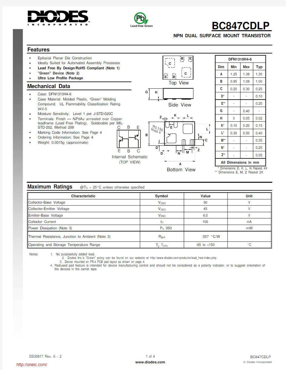
** Dimensions E, M, Z Repeat 2X
Maximum Ratings @T A = 25°C unless otherwise specified
Characteristic
Symbol Value Unit Collector-Base Voltage V CBO 50 V Collector-Emitter Voltage V CEO 45 V Emitter-Base Voltage V EBO 6.0 V Collector Current
I C
100
mA
Power Dissipation (Note 3)
P d 350 mW Thermal Resistance, Junction to Ambient (Note 3) R θJA 357 °C/W Operating and Storage Temperature Range
T j , T STG
-65 to +150
°C
Notes: 1. No purposefully added lead.
2. Diodes Inc.'s "Green" policy can be found on our website at https://www.doczj.com/doc/e615435333.html,/products/lead_free/index.php.
3. Device mounted on FR-4 PCB pad layout as shown on page
4.
4. Radiused pad feature is intended for device manufacturing control and should not be considered as a polarity indicator, or to suggest orientation of the devices in the carrier tape.
N E W P R O D U C T
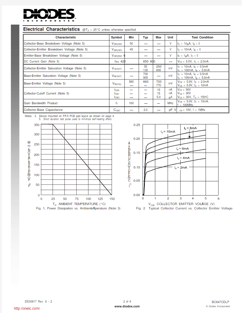
Electrical Characteristics @T A = 25°C unless otherwise specified
Characteristic
Symbol Min Typ Max Unit
Test Condition
Collector-Base Breakdown Voltage (Note 5) V (BR)CBO 50 ? ? V I C = 10μA, I B = 0 Collector-Emitter Breakdown Voltage (Note 5) V (BR)CEO
45
?
? V I C = 10mA, I B
= 0 Emitter-Base Breakdown Voltage (Note 5) V (BR)EBO 6 ? ? V
I E = 1μA, I C = 0 DC Current Gain (Note 5)
h FE 420 650 800 ?
V CE = 5.0V, I C = 2.0mA
Collector-Emitter Saturation Voltage (Note 5) V CE(SAT) ? 55 130 250600 mV
I C = 10mA, I B = 0.5mA I C = 100mA, I B = 5.0mA Base-Emitter Saturation Voltage (Note 5) V BE(SAT) ? 700 900 ? mV I C
= 10mA, I B = 0.5mA I C = 100mA, I B = 5.0mA Base-Emitter Voltage (Note 5) V BE(ON) 580 ? 660 ? 700770 mV
V CE = 5.0V, I C = 2.0mA V CE = 5.0V, I C = 10mA Collector-Cutoff Current (Note 5) I CES I CBO I CBO ? ? ? ? ? ? 15 15 5.0 nA nA μA V CE = 50V V CB = 30V
V CE = 30V, T A = 150°C
Gain Bandwidth Product f T 100 ? ? MHz V CE
= 5.0V, I C = 10mA,
f = 100MHz Collector-Base Capacitance
C CBO
?
2.0
?
pF V CB = 10V, f = 1MHz
Notes: 3. Device mounted on FR-5 PCB pad layout as shown on page 4. 5. Short duration test pulse used to minimize self-heating effect.
05010050
100
150
P , P O W E R D I S S I P A T I O N (m W )
D T , AMBIENT TEMPERATUR
E (°C)
Fig. 1, Power Dissipation vs. Ambient T emperature (Note 3)A 1502002500
30035025
75
125
I , C O L L E C T O R C U R R E N T (A )
C V , COLLECTOR EMITTER VOLT AGE (V)
Fig. 2 Typical Collector Current vs. Collector Emitter Voltage CE 0.00
0.05
0.10
0.15
0.20
0.25
1
2
3
4
5
6
N E W P R O D U C T
200400
600800100012001400
0.1
101100
h , D C C U R R E N T G A I N
F E I , COLLECTOR CURRENT (mA)
Fig. 3, Typical DC Current Gain vs. Collector Current C
110100
V , C O L L E C T O R -E M I T T E R
S A T U R A T I O N V O L T A G E (V )
C E (S A T )I , COLLECTOR CURRENT (mA)
C 0.00
0.05
0.10
0.15
0.20
0.25
0.1
Fig. 4, Typical Collector Emitter Saturation Voltage
vs. Collector Current
1
10
100
V , B A S E E M I T T E R T U R N -O N V O L T A G E (V )
B E (O N )I , COLLECTOR CURRENT (mA)
C 0.00.1
0.01
0.10.20.30.40.50.60.70.80.9
1.0Fig. 5, Typical Base Emitter Turn-On Voltage
vs. Collector Current
V , B A S E E M I T T E R S A T U R A T I O N V O L T A G E (V )
B E (S A T )I , COLLECTOR CURRENT (mA)
C 0.00.2
0.4
0.6
0.8
1.0
1.2
Fig. 6, Typical Base Emitter Saturation Voltage
vs. Collector Current
C A P A C I T A N C E (p F )
V , REVERSE VOLTAGE (V)
Fig. 7, Typical Capacitance Characteristics
R 0
2468101214
0510152025
I , COLLECTOR CURRENT (mA)
Fig. 8, Typical Gain-Bandwidth Product vs. Collector Current C 0
050
100
150
200
2503001020
30405060
70f , G A I N -B A N D W I D T H P R O D U C T (M H z )
T
N E W P R O D U C T
1M
Ordering Information (Note 6)
Notes: 6. For packaging details, please go to our website at https://www.doczj.com/doc/e615435333.html,/ap02007.pdf.
Marking Information (Note 7)
Note: 7. Package is non-polarized. Parts may be on reel in orientation illustrated, 180° rotated or mixed (both ways).
Suggested Pad Layout
IMPORTANT NOTICE
Diodes Incorporated and its subsidiaries reserve the right to make modifications, enhancements, improvements, corrections or other changes without further notice to any product herein. Diodes Incorporated does not assume any liability arising out of the application or use of any product described herein; neither does it convey any license under its patent rights, nor the rights of others. The user of products in such applications shall assume all risks of such use and will agree to hold Diodes Incorporated and all the companies whose products are represented on our website, harmless against all damages.
LIFE SUPPORT
Diodes Incorporated products are not authorized for use as critical components in life support devices or systems without the expressed written approval of the President of Diodes Incorporated.
Device Package Shipping BC847CDLP-7
DFN1310H4-6
3000/Tape & Reel
DFN1310H4-6 Dim Value X 0.52 Y 0.52 X1 0.20 Y1 0.375 X2 0.17 Y2 0.16 X3 0.15 a 0.09 b 0.06 All Dimensions in mm
1M = Product Type Marking Code
(TOP VIEW)
分销商库存信息: DIODES
BC847CDLP-7