MC33364D1R2G;MC33364D2R2G;MC33364DR2G;MC33364D1G;MC33364D2G;中文规格书,Datasheet资料
- 格式:pdf
- 大小:228.91 KB
- 文档页数:11
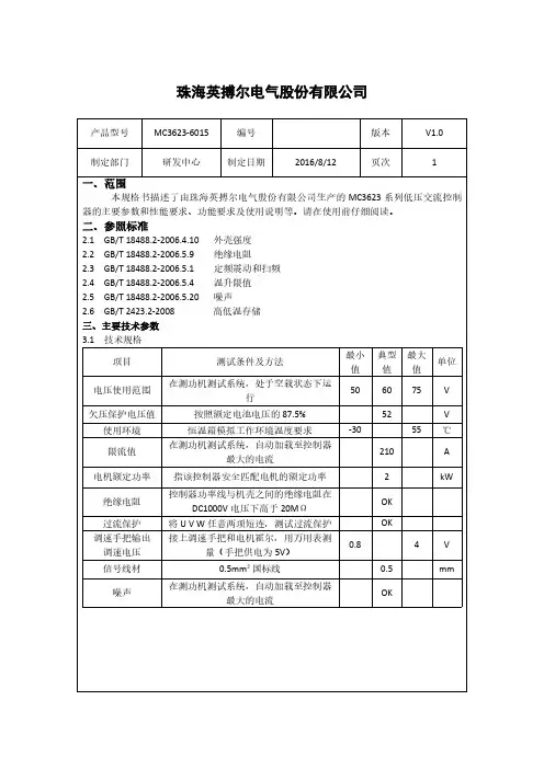
珠海英搏尔电气股份有限公司产品型号MC3623-6015编号版本V1.0制定部门研发中心制定日期2016/8/12页次1一、范围本规格书描述了由珠海英搏尔电气股份有限公司生产的MC3623系列低压交流控制器的主要参数和性能要求、功能要求及使用说明等。
请在使用前仔细阅读。
二、参照标准2.1GB/T18488.2-2006.4.10外壳强度2.2GB/T18488.2-2006.5.9绝缘电阻2.3GB/T18488.2-2006.5.1定频震动和扫频2.4GB/T18488.2-2006.5.4温升限值2.5GB/T18488.2-2006.5.20噪声2.6GB/T2423.2-2008高低温存储三、主要技术参数3.1技术规格项目测试条件及方法最小值典型值最大值单位电压使用范围在测功机测试系统,处于空载状态下运行506075V欠压保护电压值按照额定电池电压的87.5%52V 使用环境恒温箱模拟工作环境温度要求-3055℃限流值在测功机测试系统,自动加载至控制器最大的电流210A电机额定功率指该控制器安全匹配电机的额定功率2kW绝缘电阻控制器功率线与机壳之间的绝缘电阻在DC1000V电压下高于20MΩOK过流保护将U V W任意两项短连,测试过流保护OK调速手把输出调速电压接上调速手把和电机霍尔,用万用表测量(手把供电为5V)0.84V信号线材0.5mm²国标线0.5mm噪声在测功机测试系统,自动加载至控制器最大的电流OK产品型号MC3623-6015编号版本V1.0制定部门研发中心制定日期2016/8/12页次2四、控制器的外形尺寸及外观4.1外形尺寸参见附件图1-14.2外观控制器表面清洁,无明显的划痕及机械损伤,无变形,无影响控制器价值的其他外观缺陷。
五、性能5.1性能试验要求项目验证结果要求高温55℃条件下保持连续工作空载2小时,检测运行情况,再取出测试绝缘阻值。
额定电压下空载和带载启动正常恒定湿热低温-40℃存储24小时,进行测功工装测试。
MC34167 MC331671简介该MC34167, MC33167系列单片电源开关可用于dc–to–dc优化调节器申请.这些器件的固定频率,电压模式稳压器包含了所有的积极作用需要直接和实施step–down以最小的转换数量voltage–inverting外部元件.它们也可以用于成本效益在step–up转换器应用.潜在市场包括汽车,计算机,工业和成本敏感的消费产品.每一个设备的部分介绍给下面与代表框图所示图13.2振荡器振荡器频率内部编程72 kHz的电容CT和修剪电流源.该充放电率控制在产生一个95%在开关输出的最大占空比.在CT的放电,振荡器产生内部消隐脉冲持有的反相输入与门高,禁用输出开关晶体管.标称振荡器峰值和山谷门槛4.1 V和2.3 V分别.3脉宽调制器脉宽调制器由一个比较器振荡器斜坡电压施加到非反相输入端,而误差放大器的输出应用到反相输入.输出开关导通时启动CT检查排放到振荡器峰谷电压.至于收费的CT电压超过误差放大器的输出,锁存复位,终止输出晶体管的导通时间振荡器的ramp–up时期.这PWM /锁存结合防止在给定的多输出脉冲振荡器时钟周期.数字6和14说明开关输出电压与占空比的补偿.4电流检测该系列采用MC34167当前cycle–by–cycle限制,作为保护手段输出开关晶体管从过度紧张.在每个周期视为一个单独的情况.电流限制是通过监测输出开关晶体管的电流传导期间建设,并经检测过流情况,请立即关闭为振荡器的ramp–up期内开关.集电极电流转换为电压由内部微调电阻和对一个参考比较由电流检测比较器.当电流限制达到阈值,比较器重置PWM 锁存.限流门限点往往设在6.5 A.图9说明开关与输出电流限制门槛温度.5误差放大器和参考一个误差放大器的高增益提供了访问反相输入和输出.该放大器具有典型dc电压增益80 dB,和单位增益带宽600 kHz与相边缘 70度(图3).同相输入偏置内部5.05 V参考并且不固定了.参考具有精度±2.0%在室温下.以提供负载5.0 V中,参考编程50以上mV 5.0 V补偿在电缆的电压降和1.0%从连接器转换器输出.如果转换器设计需要一个输出电压高于5.05 V,电阻更大R1必须加入形成一个分压网络的反馈输入中所示数字13和18.了确定输出方程与分压网络的电压为:Vout+5.05R2R1)1外部回路补偿所需的转换器稳定.一个简单的low–pass滤波器是由连接电阻(R2)从稳压输出到反相输入,以及一系列resistor–capacitor (RF, CF)之间Pins 1和5.补偿网络的元件值显示在电路的申请被选定为each在稳定工作条件下进行测试.该step–down转换器(图18)是最容易补偿稳定.该step–up(图20)和voltage–inverting(图22)配置运作,连续导反激式转换器,而且更难以弥补.该最简单的方法来优化网络是补偿观察输出电压的负载响应一步变化,而调整临界阻尼RF和CF.该最终电路应验证以下四个稳定边界条件.这些条件是最小和最大输入电压,最小和最大负载.通过箝位的电压误差放大器的输出(引脚5)不到150 mV,内部电路将放置到一个低功耗待机模式,从而将权力电源电流36µA与12 V电源电压.图10说明了备用电源电流与电源电压.误差放大器的输出有一个100µA电流源pull–up,可用于实现soft–start.图17显示充电电流源通过一个电容CSS系列二极管.该二极管断开从反馈CSS回路电阻时1.0 M操作它上面的收费销5.范围开关输出输出开关晶体管的设计最大的40 V,以最小的峰值集电极电流时5.5 A.配置为step–down或voltage–inverting应用,如在图18和22,电感会把偏置的输出整流开关关闭时.整流器与较高的正向电压降或长期拖延的时间应该打开不能使用.如果发射器被允许去充分负,集电极电流流过,造成额外的装置暖气,降低转换效率.图8显示到箝位的发射器0.5集电极电流V,在一系列的100µA温度过高.阿1N5825或肖特基势垒整流器相当于推荐履行这些要求.欠压分离欠压分离一直比较成立以保证完全集成电路在输出级的功能已启用.内部参考电压比较器的监测使输出阶段VCC超过5.9 V.为了防止不稳定的输出交叉切换的阈值,0.9 V迟滞.6摩托罗拉设备数据模拟ICMC34167 MC33167热保护内部热关断电路,以保护在事件集成电路的最大结温度超过.当被激活时,通常在170°C,是被迫的锁存成'复位'的状态,关闭输出开关.此功能防止灾难性故障提供偶然的设备过热.它的目的不是要作为一个适当的散热片的替代品.该MC34167包含在5–lead TO–220类型包装.该标签包装是很常见的中心引脚(引脚3),通常连接到地.设计考虑不要试图建立一个转换器上wire–wrap或plug–in原型板.特别应注意分开的信号电流和接地接地通路从负载电流路径.所有高电流回路应尽可能短尽可能使用重型铜runs到尽量减少振荡和辐射EMI.为了获得最佳的操作,严密元件布局建议.电容器Cin, CO,和所有的反馈元件应尽可能靠近IC在身体可能.这也是必须的肖特基二极管连接到开关输出是尽可能靠近尽可能IC.图15.低功耗待机电路+100µA错误放大器1图16.过电压关断电路+100µA错误放大器1120补偿5120补偿R15R1I =待机模式VShutdown = VZener + 0.7图17. Soft–Start电路+100µA错误放大器1120补偿D2Vin1.0 MCss5D1R1tSoft–Start≈35,000 Css。
F SUFFIXPLASTIC EIAJ SOIC PACKAGECASE 965–01ISSUE ONOTES:1.DIMENSIONING AND TOLERANCING PER ANSI Y14.5M, 1982.ON Semiconductor and are trademarks of Semiconductor Components Industries, LLC (SCILLC). SCILLC reserves the right to make changeswithout further notice to any products herein. SCILLC makes no warranty, representation or guarantee regarding the suitability of its products for any particular purpose, nor does SCILLC assume any liability arising out of the application or use of any product or circuit, and specifically disclaims any and all liability,including without limitation special, consequential or incidental damages. “Typical” parameters which may be provided in SCILLC data sheets and/or specifications can and do vary in different applications and actual performance may vary over time. All operating parameters, including “Typicals” must be validated for each customer application by customer’s technical experts. SCILLC does not convey any license under its patent rights nor the rights of others.SCILLC products are not designed, intended, or authorized for use as components in systems intended for surgical implant into the body, or other applications intended to support or sustain life, or for any other application in which the failure of the SCILLC product could create a situation where personal injury or death may occur. Should Buyer purchase or use SCILLC products for any such unintended or unauthorized application, Buyer shall indemnify and hold SCILLC and its officers, employees, subsidiaries, affiliates, and distributors harmless against all claims, costs, damages, and expenses, and reasonable attorney fees arising out of, directly or indirectly, any claim of personal injury or death associated with such unintended or unauthorized use, even if such claim alleges that SCILLC was negligent regarding the design or manufacture of the part. SCILLC is an Equal Opportunity/Affirmative Action Employer.PUBLICATION ORDERING INFORMATIONCENTRAL/SOUTH AMERICA:Spanish Phone :303–308–7143 (Mon–Fri 8:00am to 5:00pm MST)Email :ONlit–spanish@ ASIA/PACIFIC : LDC for ON Semiconductor – Asia SupportPhone :303–675–2121 (Tue–Fri 9:00am to 1:00pm, Hong Kong Time)Toll Free from Hong Kong & Singapore:001–800–4422–3781Email : ONlit–asia@JAPAN : ON Semiconductor, Japan Customer Focus Center4–32–1 Nishi–Gotanda, Shinagawa–ku, Tokyo, Japan 141–8549Phone : 81–3–5740–2745Email : r14525@。
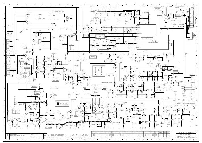
0123456789A B C D E F G H I J K L M N O P Q R S T U V W123456789A B C D E F G HI JKL M N O P Q RS TUV WREV/ISS AMENDMENTS DATEAPVD D.O.CHKD DRAWN TAIT ELECTRONICS2.SC.12T2000-500/600 UHF MOBILE RADIODUAL BAND RETROFIT OPTION120518c 220-01205-183-Jul-00C T2000-500/600TS 11A MODS TO PWR CONTROL ETC.M.C.8AADDED LOW-POWER VARIANTSJ.F.J.F.22/2/930V-AT-REST8B MODIFIED VARIANTS-TABLE FOR C327 & C329, SHEET-2.J.F.J.F.S.P.14/5/938C MODIFIED NOISE BLANKER VARIANTS CH/N 93/03-118.M.C.G.S.18/5/938D NO CONNECTIVITY CHANGES.M.C.G.S. D.E.M.B.14/7/93RX:7V5TX:0V 9A UPDATED PA, SYNTH. ADDED VIAS AROUND EDGE OF PCB.M.C.K.B. D.E.M.B.28/8/939B UPDATED EXCITER AND SYNTH LAYOUT.M.C.RX 3V013V0CONTROL-VOLTS+5DBM/50OHM+6DBM/50OHMTX:+4V5RX:+3V3FREQ 400470RX:0V TX:20V10AADDED Q217, Q309 & OTHER ASSORTED MODS.J.F.J.F.10/8/9413ADDED D305,R348,#334,#C365,C318A,C500.YH 14-3-952V7-6V7TYP:*****************1V0.P-P 60%-MODTYP:**********************TX 3V212V814EMC MOD BY DECOUPLING P3 WITH 1N0 CAPS YH 11/10/9518A ADD DUAL BAND OPTION ECO 21-0491TS 31-03-0018B REMOVED TEXT LINE FROM PLC FILE TS 20-06-0018C ECO21-0582 CHANGED R319 TO R331TS 3-7-00*C10110P*C1074P7*C11018P*C1115P6*C11418P*C1158P2*C11918P*C1215P6*C1224P7*C2275P6 *C2326P8 *C2375P6*C23818P *C3026P8 *C30810P*C30922P*C31410P*C32133P*C 32233P*C3314P7*C33210P *C3352P2*C3393P9*C3413P9*C3423P3*C3433P9*C3462P2*C3472P2*C3503P3*C3521P2 *C 3651U 0*L207#570*L3001T/2.5*L3021.5T/2.5*L314#4S3B *L3221.5T/4.0 *L3241.5T/4.0 *L3251.5T/4.0*L3261.5T/4.0*R304100*R30968*R313330 1%*R31456*R31522*R31856R32333*R 33422#C 152A10N#C153A 100P #C156#D140A BAT18 #Q108BFS17#R14068K#R140A 33K#R14227K#R142A 100K#R143A 33K#R14468K#R144A 120K#R145A 33K C110NC100150PC102150PC104100NC1051P0C10633PC108150PC1092P2C1121P5 C1132P2C1171P5C1182P2C123150PC1245P6C1252P7C1265P6C12712PC12833PC12910NC13010NC132150PC13347PC1346P8 C13533PC1366P8 C137100PC1386P8C13933PC1406P8 C14147PC14212PC145100PC1461N0C14710NC14810PC149150PC150100P C151100NC152100P C1534U7C15410NC155100PC157100NC1581N0C17447UC175100NC176100NC17910NC180100NC181100NC182150PC184150PC18510NC18610NC1871N0C188100PC189470P C190470PC1911N0 C19233PC1934U7C194150PC195150PC197100NC1981P0C1991N0C21N0C20010NC20147NC20222P C204150PC20522NC206100NC20710NC20810N C20910NC21010N C211180P C2125P6C21347UC21410NC2154U7C21610NC21747UC2184U7C2194U7C22010NC2211U0 C222100NC2234U7C223A 8P2C2241N0C225150PC226150PC22822N C22947UC23010NC23110NC2334U7C2344U7C235100NC236150PC2391P0C240150PC241150PC24210NC243150PC2445P6 C2452P7C24610NC2478P2C24810NC249100PC25082P C251100P C252180PC25382PC254150PC2555P6C25718PC2604U7C31N0C300100P C301150P C30310PC3041N0 C30512P C30622P C307100N C3101N0C311150PC312150PC313150P C315150PC316150P C317150PC318150PC318A 12PC319100PC32033PC326100PC3284U7C333150P C 334150PC336100PC337150PC33810P C3403P9C3443P3C345150PC348150PC349150P C351100N C3531N0C35510NC356150PC357100NC35815PC359100NC360150PC3618P2C36233PC36333PC3641N0 C403470PC4104U7C411100NC41247U C413100NC414470U C4151000UC4161N0C419100NC420100NC42356U C4244U7C4254U7C42610NC4274U7C4284U7C4291N0C43056UC431100NC4511N0C4551N0C5000805D1MR2520D100BAV9931D100BAV9923D101BBY40 23D102BBY40 23D103BBY4023D105BAT18D106BAT18D107BAT17DS23D107BAT17DS31D108BAT17DS31D108BAT17DS23 BAT17DS D11031 BAT17DS D11023 BAT17DS D11123 BAT17DS D11131D202BAV7013D203BBY40 23D204BBY42 23D205BBY4023D206BBY4223D208BAT18D209BAT18 D210BAT18D211BAT18 D3011SS97D303UM9401 D304UM9401BAV70D30513 BAV70D30523D401BAV70 23D401BAV7013ININ OUT PD OUTR VSYNTHESISERIC201145158-2F 8DATA 10CLK9EN11GND 6F 13F 3OSC 1OSC 2REF 14MC 12+V 4LD 7OUT5PR 16PV 15IC203MC12052IN1GND 5IN 8SW 3NC 7VCC 2MC6OUT 4VREG IC4037808ACTVIN 1GND2VOUT3VREG IC4047805ACTVIN 1GND2VOUT3VREG IC405LM317LVIN3ADJ2VOUT 1L1#4S3BL104#664L105#664L106#664 L107RF BALUN32146L108RF BALUN32146L1091.5T/3.0 L110330NL114#662L116#662L117RF BALUN32146L118RF BALUN32146L119#655 23614L120M21B L121M21AL200M21B L201100NHL202100NH L203#662L204100NHL205330NHL206330NHL208330NHL209330NH L21015NHL30115NHL315330NH L303330NL304#4S3B L30515NHL306M21BL307#4S3BL3086.5T/3.0L309#4S3B L3106.5T/3.0 L3116.5T/3.0L312330NHL3135.5T/4.5 L3181.5T/2.5L319330NL3202.5T/3.5L3231.5T/3.5 L331M21BL401#650 23614P 8P9Q101951Q102BC857Q103951Q105951Q106BCW72Q107BFS17Q109BF824 Q110BFS17 Q115BCW72Q200BCW72Q201BC857Q202BCW72Q203BCW72Q204BCW72Q205BC857Q206BCW72Q207BC857Q208BCW72Q209BC857Q211BC807Q212951 Q213BCW72Q214MMBR571 Q215MMBR571Q216BCW72Q217BCW72Q300MS1649Q301951Q302MRF559Q303BCW72 Q304BD234Q305MRF653Q307BCW72Q308BC807Q309951 Q310BCW72Q311BC807 Q401BC857Q402BC817CWRV15347K231CWRV22247K231C WRV324470K231R100470 R1013K9 R102560R1032K2R104120R10518 R106100KR107100KR108100KR11247 R1134R7R114820R11512KR1164R7R11710R118100 R11910R120820R121180R12210KR12310KR131100R1322K2R133270 R13510KR138100K R1411K5R14333KR1451K5R14622 R147220R148560R150100KR1513K3R152390KR1531K0R155100KR156100R15710KR1581K0R15947R16010 R1611K0 R1940R19568KR196100R197100R1982K2R199100R2000R2092K2R210180KR2121K8R2131K2R2141K2R21747R21812KR219330R2206K8R221330 R22247R22322KR22412KR22522KR2265K6R227220R2283K3 R22922R230470 R231220R2322K2 R2331M0R23468 R235330R23647R237100R2388K2R23922K R240100KR2411K8R24222R2433K3R24422R245100R246390R24710 R2480R25022R251150R252820R25333R25433R25522 R2561K5R2571K2R25810R259820R26018R26133R26222KR26347K R26422KR265100K R2663K3R2673K3 R26856ER2694R7R27047R27110R272220R2734R7R2743K9R27547R2766K8R27747 R278100KR279180K R280180KR282120 R28410KR28510K R2861K0R287100KR2880R2901K0R300220R301220R3021K0R30368R30510R3061K2 *R307150ER3081K2 R310220 R311180 R312680 R316150R317100R32027KR321470KR32210R32418R32527KR326220KR3271K0R328150R32947KR330220KR332100R3332K2R3370R33833K R33910KR34010KR34147K R342150KR3434K7R3442K2R3451K0 R346680 R34710K R3481K0R418680R42039K R42139KR42222R4251K0R4264R7R4274R7R42822R42927KR4306K8R431100KR43210R433100R43422 R43518KR4361K2R4371K0S4I/OPADTSP5TSP7IC1013371D1011OUT IN IC1013371DLIM 5GND 15VCC 4DEC 6DEC 7QUAD 8AF9RSSI13IC1013371D1214+-IC20233078D321+-IC20233078D5671020IC402+6GND 9SUB1SB5VCC3BS 4O/P2D202BAV70 23P15 P13P12R1280R162100Q121BCW72C131470PR1492K2R1302K2P14 P17P16R33147D307MA4P1250D306MA4P1250 D SGQ100BFR31D S GQ210BFR31P18P19+1020IC40287P20P10 P11R1261K0C11615NP1+5V15P1+8V10P1+8V-SYNTH9P1AF-SIG8P1BUSY3P1CLK12P1DATA13P1DET-AF5P1ENABLE14P1GND4P1GND1P1GND16P1LCK-DET11P1LF-SIG6P1MOD7P1RSSI2P2+13.8V 8P2+13.8V-US6P2+13V-ECON 5P2+5-VOLTS7P2+8V-CNTRL 9P2+8VTX 10P2AUDIO-PA1P2EXTRNL3P2GND2P2IGN4P2PWR-CNTRL12P2PWR-SENSE 11P3AUDIO4P3EXTRNL 1P3GND 5P3GND 3P3IGN 7P3SPKR 2P313.8V-UNSW6P5+8VOLTS7P5AF-OUT 10P5CMPRTR-OUT 6P5DETECT-AUDIO8P5FILTER3P5GND2P5MIXER4P5NSE-DET5P5QUAD-COIL 1P5455-OUT 9P6+8V-SYNTH10P6+8V-SYNTH4P6TCXO1P6AF-SIG 9P6GND2P6GND3P6LF-SIG 7P6MOD 6P6REF-MOD5P6TX-AF 8P7INT 2P7SPKR 1+13.8V +13.8V+13.8V-UNSW+13.8V-UNSW+13.8V-UNSW+13V-ECON +13V-ECON+13V-Q306+21V+21V+21V+5-VOLTS+5-VOLTS+5V+5V+5V+8-VOLTS+8-VOLTS+8-VOLTS+8-VOLTS+8-VOLTS +8-VOLTS+8V+8V+8V+8V+8V-CNTRL+8V-CNTRL+8V-CNTRL+8V-SYNTH+8V-SYNTH+8V-SYNTH+8V-SYNTH+8V-TX+8V-TXRF-INRF-OUTREF-MOD ADJSYNTHESISERLOOP FILTERTCXO & TX-AUDIO PCBDELAY LINE+8V-TXRX-TUNE VOLTAGEPDL16MPDL12MP1 TO CONTROL PCBP2 TO CNTRL PCBIF PCB32161P R I N T E DBASE LNOT FITTED FOR HIGH-BAND+8V-TXUNDER-WALL DECOUPLING4S34S3*84TO LOOM CONNECTOR P2PIN-7*NOISE BLANKERPA OPTION: 25W-Q306 OR LOW-POWER VERSIONFOR LOW-POWER VERSION,(SEE SHEET-2 FOR OPTION CCT-DETAILS)*LINK FOR LOW-PWR VERSIONSLOW POWER VERSIONS)(IPN 220-01287-00)*R315 NOT FITTED FOR HIGH-BANDUSE DUMMY-TRANSISTOR PCBFROM +8V REGULATOR ON CNTRL PCB, VIA P1-PIN 9(IPN:220-01201-00)X3 MULTIPLIERVCOFROM +21V REGULATOR, IC405PRESCALERFROM P2/PIN-10(VIA L331)20NHPRTDPRINTED *C322 NOT FITTED FOR LOW-BAND PRINTED *1ST MIXERTO LOOP-FILTERIC202 PIN-8+21V & Q213 IN VCO87AUDIO PAFROM CNTRL PCB +13.8V-ECONOMY VIA P2-PIN 5TO LOOM CONNECTOR P2 PIN-6& RF POWER-AMP(IPN:220-01201-00)TRACK-FUSEPCB-GND INTERNAL SPKRPL2USPKRGNDSK7HMCHC U T F O R E X T R N L S P K RGNDL304, L307, L314, L316 & L309NOT FITTED FOR COUPLERHIGH-BAND*C352 NOT FITTED FOR HIGH-BAND( ,CRUSH BEADS FOR*DUAL-4S3B BEADSTO CNTRL-PCB VIA P2 PIN-9 & Q311SUB-PCB **PRINTED RF-OUT38.4MHZTCXO-MODAF-OUTDET-AFFILTERQ131-C Q131-B+8VGNDP9REF-MOD#682#674P20P10AF-OUT2AF-OUT2TCXO-MOD2TCXO-MOD212312312312312312312312312312312312312345678912345678912121212121234567123456712345671234567890121234567890121234567890121231231231231231231112345678912345678912345678912345678912345678912345678912345678912345678912345678123456781234567812345678123456781234567890121234567890121234567890121234567890121234567890123456789012345678901234567890123456789012345678901212345678901234567890123456789012123456789012345678901234567890121231234567890123456789012345678901212345678901234567890123456789012123456789012345678901234567890121231234567890123456789012345678901212345678901234567890123456789012123456789012345678901234567890121231234567890123456789012345678901212345678901234567890123456789012123456789012345678901234567890121231234567890123456789012345678901212345678901234567890123456789012123456789012345678901234567890121231234567890123456789012345678901212345678901234567890123456789012123456789012345678901234567890121231234567890123456789012345678901212345678901234567890123456789012123456789012345678901234567890121231234567890123456789012345678901212345678901234567890123456789012123456789012345678901234567890121231234567890123456789012345678901212345678901234567890123456789012123456789012345678901234567890121231234567890123456789012345678901212345678901234567890123456789012123456789012345678901234567890121231234567890123456789012345678901212345678901234567890123456789012123456789012345678901234567890121231234567890123456789012345678901212345678901234567890123456789012123456789012345678901234567890121231234567890123456789012345678901212345678901234567890123456789012123456789012345678901234567890121231234567890123456789012345678901212345678901234567890123456789012123456789012345678901234567890121231234567890123456789012345678901212345678901234567890123456789012123456789012345678901234567890121231234567890123456789012345678901212345678901234567890123456789012123456789012345678901234567890121231234567890123456789012345678901212345678901234567890123456789012123456789012345678901234567890121231234567890123456789012345678901212345678901234567890123456789012123456789012345678901234567890121231234567890123456789012345678901212345678901234567890123456789012123456789012345678901234567890121231234567890123456789012345678901212345678901234567890123456789012123456789012345678901234567890121231234567890123456789012345678901212345678901234567890123456789012123456789012345678901234567890121231234567890123456789012345678901212345678901234567890123456789012123456789012345678901234567890121231234567890123456789012345678901212345678901234567890123456789012123456789012345678901234567890121231234567890123456789012345678901212345678901234567890123456789012123456789012345678901234567890121231234567890123456789012345678901212345678901234567890123456789012123456789012345678901234567890121231234567890123456789012345678901212345678901234567890123456789012123456789012345678901234567890121231234567890123456789012345678901212345678901234567890123456789012123456789012345678901234567890121231234567890123456789012345678901212345678901234567890123456789012123456789012345678901234567890121231234567890123456789012345678901212345678901234567890123456789012123456789012345678901234567890121231234567890123456789012345678901212345678901234567890123456789012123456789012345678901234567890121231234567890123456789012345678901212345678901234567890123456789012123456789012345678901234567890121231234567890123456789012345678901212345678901234567890123456789012123456789012345678901234567890121231234567890123456789012345678901212345678901234567890123456789012123456789012345678901234567890121231234567890123456789012345678901212345678901234567890123456789012123456789012345678901234567890121231234567812345678123456781234567812345678123456781234567812345678123456789123456789123456789123456789123456789123456789123456789123456789123456789012345678901234567890121234567890123456789012345678901212345678901234567890123456789012123456789012345678901234567890121234567890112345678901234567890123456789012123456789012345678901234567890121234567890123456789012345678901212345678901234567890123456789012123456789011234567890123456789012345678901212345678901234567890123456789012123456789012345678901234567890121234567890123456789012345678901212345678901123456789012345678901234567890121234567890123456789012345678901212345678901234567890123456789012123456789012345678901234567890121234567890112345678901234567890123456789012123456789012345678901234567890121234567890123456789012345678901212345678901234567890123456789012123456789011234567890123456789012345678901212345678901234567890123456789012123456789012345678901234567890121234567890123456789012345678901212345678901123456789012345678901234567890121234567890123456789012345678901212345678901234567890123456789012123456789012345678901234567890121234567890112345678901234567890123456789012123456789012345678901234567890121234567890123456789012345678901212345678901234567890123456789012123456789011234567890123456789012345678901212345678901234567890123456789012123456789012345678901234567890121234567890123456789012345678901212345678901123456789012345678901234567890121234567890123456789012345678901212345678901234567890123456789012123456789012345678901234567890121234567890112345678901234567890123456789012123456789012345678901234567890121234567890123456789012345678901212345678901234567890123456789012123456789011234567890123456789012345678901212345678901234567890123456789012123456789012345678901234567890121234567890123456789012345678901212345678901123456789012345678901234567890121234567890123456789012345678901212345678901234567890123456789012123456789012345678901234567890121234567890112345678901234567890123456789012123456789012345678901234567890121234567890123456789012345678901212345678901234567890123456789012123456789011234567890123456789012345678901212345678901234567890123456789012123456789012345678901234567890121234567890123456789012345678901212345678901123456789012345678901234567890121234567890123456789012345678901212345678901234567890123456789012123456789012345678901234567890121234567890112345678901234567890123456789012123456789012345678901234567890121234567890123456789012345678901212345678901234567890123456789012123456789011234567890123456789012345678901212345678901234567890123456789012123456789012345678901234567890121234567890123456789012345678901212345678901123456789012345678901234567890121234567890123456789012345678901212345678901234567890123456789012123456789012345678901234567890121234567890112345678901234567890123456789012123456789012345678901234567890121234567890123456789012345678901212345678901234567890123456789012123456789011234567890123456789012345678901212345678901234567890123456789012123456789012345678901234567890121234567890123456789012345678901212345678901123456789012345678901234567890121234567890123456789012345678901212345678901234567890123456789012123456789012345678901234567890121234567890112345678901234567890123456789012123456789012345678901234567890121234567890123456789012345678901212345678901234567890123456789012123456789011234567890123456789012345678901212345678901234567890123456789012123456789012345678901234567890121234567890123456789012345678901212345678901123456789012345678901234567890121234567890123456789012345678901212345678901234567890123456789012123456789012345678901234567890121234567890112345678901234567890123456789012123456789012345678901234567890121234567890123456789012345678901212345678901234567890123456789012123456789011234567890123456789012345678901212345678901234567890123456789012123456789012345678901234567890121234567890123456789012345678901212345678901123456789012345678901234567890121234567890123456789012345678901212345678901234567890123456789012123456789012345678901234567890121234567890112345678901234567890123456789012123456789012345678901234567890121234567890123456789012345678901212345678901234567890123456789012123456789011234567890123456789012345678901212345678901234567890123456789012123456789012345678901234567890121234567890123456789012345678901212345678901123456789012345678901234567890121234567890123456789012345678901212345678901234567890123456789012123456789012345678901234567890121234567890112345678901234567890123456789012123456789012345678901234567890121234567890123456789012345678901212345678901234567890123456789012123456789011234567890123456789012345678901212345678901234567890123456789012123456789012345678901234567890121234567890123456789012345678901212345678901123456789012345678901234567890121234567890123456789012345678901212345678901234567890123456789012123456789012345678901234567890121234567890112345678901234567890123456789012123456789012345678901234567890121234567890123456789012345678901212345678901234567890123456789012123456789011234567890123456789012345678901212345678901234567890123456789012123456789012345678901234567890121234567890123456789012345678901212345678901123456789012345678901234567890121234567890123456789012345678901212345678901234567890123456789012123456789012345678901234567890121234567890112345678901234567890123456789012123456789012345678901234567890121234567890123456789012345678901212345678901234567890123456789012123456789011234567890123456789012345678901212345678901234567890123456789012123456789012345678901234567890121234567890123456789012345678901212345678901123456789012345678901234567890121234567890123456789012345678901212345678901234567890123456789012123456789012345678901234567890121234567890112345678901234567890123456789012123456789012345678901234567890121234567890123456789012345678901212345678901234567890123456789012123456789011234567890123456789012345678901212345678901234567890123456789012123456789012345678901234567890121234567890123456789012345678901212345678901123456789012345678901234567890121234567890123456789012345678901212345678901234567890123456789012123456789012345678901234567890121234567890112345678901234567890123456789012123456789012345678901234567890121234567890123456789012345678901212345678901234567890123456789012123456789011234567890123456789012345678901212345678901234567890123456789012123456789012345678901234567890121234567890123456789012345678901212345678901123456789012345678901234567890121234567890123456789012345678901212345678901234567890123456789012123456789012345678901234567890121234567890112345678901234567890123456789012123456789012345678901234567890121234567890123456789012345678901212345678901234567890123456789012123456789011234567890123456789012345678901212345678901234567890123456789012123456789012345678901234567890121234567890123456789012345678901212345678901123456789012345678901234567890121234567890123456789012345678901212345678901234567890123456789012123456789012345678901234567890121234567890112345678901234567890123456789012123456789012345678901234567890121234567890123456789012345678901212345678901234567890123456789012123456789011234567890123456789012345678901212345678901234567890123456789012123456789012345678901234567890121234567890123456789012345678901212345678901123456789012345678901234567890121234567890123456789012345678901212345678901234567890123456789012123456789012345678901234567890121234567890112345678901234567890123456789012123456789012345678901234567890121234567890123456789012345678901212345678901234567890123456789012123456789011234567890123456789012345678901212345678901234567890123456789012123456789012345678901234567890121234567890123456789012345678901212345678901123456789012345678901234567890121234567890123456789012345678901212345678901234567890123456789012123456789012345678901234567890121234567890112345678901234567890123456789012123456789012345678901234567890121234567890123456789012345678901212345678901234567890123456789012123456789011234567890123456789012345678901212345678901234567890123456789012123456789012345678901234567890121234567890123456789012345678901212345678901123456789012345678901234567890121234567890123456789012345678901212345678901234567890123456789012123456789012345678901234567890121234567890112345678901234567890123456789012123456789012345678901234567890121234567890123456789012345678901212345678901234567890123456789012123456789011234567890123456789012345678901212345678901234567890123456789012123456789012345678901234567890121234567890123456789012345678901212345678901123456789012345678901234567890121234567890123456789012345678901212345678901234567890123456789012123456789012345678901234567890121234567890112345678901234567890123456789012123456789012345678901234567890121234567890123456789012345678901212345678901234567890123456789012123456789011234567890123456789012345678901212345678901234567890123456789012123456789012345678901234567890121234567890123456789012345678901212345678901123456789012345678901234567890121234567890123456789012345678901212345678901234567890123456789012123456789012345678901234567890121234567890112345678901234567890123456789012123456789012345678901234567890121234567890123456789012345678901212345678901234567890123456789012123456789011234567890123456789012345678901212345678901234567890123456789012123456789012345678901234567890121234567890123456789012345678901212345678901123456789012345678901234567890121234567890123456789012345678901212345678901234567890123456789012123456789012345678901234567890121234567890112345678901234567890123456789012123456789012345678901234567890121234567890123456789012345678901212345678901234567890123456789012123456789011234567890123456789012345678901212345678901234567890123456789012123456789012345678901234567890121234567890123456789012345678901212345678901123456789012345678901234567890121234567890123456789012345678901212345678901234567890123456789012123456789012345678901234567890121234567890112345678901234567890123456789012123456789012345678901234567890121234567890123456789012345678901212345678901234567890123456789012123456789011234567890123456789012345678901212345678901234567890123456789012123456789012345678901234567890121234567890123456789012345678901212345678901123456789012345678901234567890121234567890123456789012345678901212345678901234567890123456789012123456789012345678901234567890121234567890112345678901234567890123456789012123456789012345678901234567890121234567890123456789012345678901212345678901234567890123456789012123456789011234567890123456789012345678901212345678901234567890123456789012123456789012345678901234567890121234567890123456789012345678901212345678901123456789012345678901234567890121234567890123456789012345678901212345678901234567890123456789012123456789012345678901234567890121234567890112345678901234567890123456789012123456789012345678901234567890121234567890123456789012345678901212345678901234567890123456789012123456789011234567890123456789012345678901212345678901234567890123456789012123456789012345678901234567890121234567890123456789012345678901212345678901123456789012345678901234567890121234567890123456789012345678901212345678901234567890123456789012123456789012345678901234567890121234567890112345678901234567890123456789012123456789012345678901234567890121234567890123456789012345678901212345678901234567890123456789012123456789011212121212121212121212121212121212121212121212345123451234512345678901212345678901212345678901212345678901212345678901212345678901212345678901212345678901212345678901212345678901234567890123456789012123456789012345678901234567890121234567890123456789012345678901234567890123456789012345678901212345678901234567890123456789012123456789012345678901234567890123456789012345678901234567890121234567890123456789012345678901212345678901234567890123456789012345678901234567890123456789012123456789012345678901234567890121234567890123456789012345678901234567890123456789012345678901212345678901234567890123456789012123456789012345678901234567890123456789012345678901234567890121234567890123456789012345678901212345678901234567890123456789012345678901234567890123456789012123456789012345678901234567890121234567890123456789012345678901234567890123456789012345678901212345678901234567890123456789012123456789012345678901234567890123456789012345678901234567890121234567890123456789012345678901212345678901234567890123456789012345678901234567890123456789012123456789012345678901234567890121234567890123456789012345678901234567890123456789012345678901212345678901234567890123456789012123456789012345678901234567890123456789012345678901234567890121234567890123456789012345678901212345678901234567890123456789012345678901234567890123456789012123456789012345678901234567890121234567890123456789012345678901234567890123456789012345678901212345678901234567890123456789012123456789012345678901234567890123456789012345678901234567890121234567890123456789012345678901212345678901234567890123456789012345678901234567890123456789012123456789012345678901234567890121234567890123456789012345678901234567890123456789012345678901212345678901234567890123456789012123456789012345678901234567890123456789012345678901234567890121234567890123456789012345678901212345678901234567890123456789012345678901234567890123456789012123456789012345678901234567890121234567890123456789012345678901234567890123456789012345678901212345678901234567890123456789012123456789012345678901234567890123456789012345678901234567890121234567890123456789012345678901212345678901234567890123456789012345678901234567890123456789012123456789012345678901234567890121234567890123456789012345678901234567890123456789012345678901212345678901234567890123456789012123456789012345678901234567890123456789012345678901234567890121234567890123456789012345678901212345678901234567890123456789012345678901234567890123456789012123456789012345678901234567890121234567890123456789012345678901234567890123456789012345678901212345678901234567890123456789012123456789012345678901234567890123456789012345678901234567890121234567890123456789012345678901212345678901234567890123456789012345678901234567890123456789012123456789012345678901234567890121234567890123456789012345678901234567890123456789012345678901212345678901234567890123456789012123456789012345678901234567890123456789012345678901234567890121234567890123456789012345678901212345678901234567890123456789012345678901234567890123456789012123456789012345678901234567890121234567890123456789012345678901234567890123456789012345678901212345678901234567890123456789012123456789012345678901234567890123456789012345678901234567890121234567890123456789012345678901212345678901234567890123456789012345678901234567890123456789012123456789012345678901234567890121234567890123456789012345678901234567890123456789012345678901212345678901234567890123456789012123456789012345678901234567890123456789012345678901234567890121234567890123456789012345678901212345678901234567890123456789012345678901234567890123456789012123456789012345678901234567890121234567890123456789012345678901234567890123456789012345678901212345678901234567890123456789012123456789012345678901234567890123456789012345678901234567890121234567890123456789012345678901212345678901234567890123456789012345678901234567890123456789012123456789012345678901234567890121234567890123456789012345678901234567890123456789012345678901212345678901234567890123456789012123456789012345678901234567890123456789012345678901234567890121234567890123456789012345678901212345678901234567890123456789012345678901234567890123456789012123456789012345678901234567890121234567890123456789012345678901234567890123456789012345678901212345678901234567890123456789012123456789012345678901234567890123456789012345678901234567890121234567890123456789012345678901212345678901234567890123456789012345678901234567890123456789012123456789012345678901234567890121234567890123456789012345678901234567890123456789012345678901212345678901234567890123456789012123456789012345678901234567890123456789012345678901234567890121234567890123456789012345678901212345678901234567890123456789012345678901234567890123456789012123456789012345678901234567890121234567890123456789012345678901234567890123456789012345678901212345678901234567890123456789012123456789012345678901234567890123456789012345678901234567890121234567890123456789012345678901212345678901234567890123456789012345678901234567890123456789012123456789012345678901234567890121234567890123456789012345678901234567890123456789012345678901212345678901234567890123456789012123456789012345678901234567890123456789012345678901234567890121234567890123456789012345678901212345678901234567890123456789012345678901234567890123456789012123456789012345678901234567890121234567890123456789012345678901234567890123456789012345678901212345678901234567890123456789012123456789012345678901234567890123456789012345678901234567890121234567890123456789012345678901212345678901234567890123456789012345678901234567890123456789012123456789012345678901234567890121234567890123456789012345678901234567890123456789012345678901212345678901234567890123456789012123456789012345678901234567890123456789012345678901234567890121234567890123456789012345678901212345678901234567890123456789012345678901234567890123456789012123456789012345678901234567890121234567890123456789012345678901234567890123456789012345678901212345678901234567890123456789012123456789012345678901234567890123456789012345678901234567890121234567890123456789012345678901212345678901234567890123456789012345678901234567890123456789012123456789012345678901234567890121234567890123456789012345678901234567890123456789012345678901212345678901234567890123456789012123456789012345678901234567890123456789012345678901234567890121234567890123456789012345678901212345678901234567890123456789012345678901234567890123456789012123456789012345678901234567890121234567890123456789012345678901234567890123456789012345678901212345678901234567890123456789012123456789012345678901234567890123456789012345678901234567890121234567890123456789012345678901212345678901234567890123456789012345678901234567890123456789012123456789012345678901234567890121234567890123456789012345678901234567890123456789012345678901212345678901234567890123456789012123456789012345678901234567890123456789012345678901234567890121234567890123456789012345678901212345678901234567890123456789012345678901234567890123456789012123456789012345678901234567890121234567890123456789012345678901234567890123456789012345678901212345678901234567890123456789012123456789012345678901234567890123456789012345678901234567890121234567890123456789012345678901212345678901234567890123456789012345678901234567890123456789012123456789012345678901234567890121234567890123456789012345678901234567890123456789012345678901212345678901234567890123456789012123456789012345678901234567890123456789012345678901234567890121234567890123456789012345678901212345678901234567890123456789012345678901234567890123456789012123456789012345678901234567890121234567890123456789012345678901234567890123456789012345678901212345678901234567890123456789012123456789012345678901234567890123456789012345678901234567890121234567890123456789012345678901212345678901234567890123456789012345678901234567890123456789012123456789012345678901234567890121234567890123456789012345678901234567890123456789012345678901212345678901234567890123456789012123456789012345678901234567890123456789012345678901234567890121234567890123456789012345678901212345678901234567890123456789012345678901234567890123456789012123456789012345678901234567890121234567890123456789012345678901234567890123456789012345678901212345678901234567890123456789012123456789012345678901234567890123456789012345678901234567890121234567890123456789012345678901212345678901234567890123456789012345678901234567890123456789012123456789012345678901234567890121234567890123456789012345678901234567890123456789012345678901212345678901234567890123456789012123456789012345678901234567890123456789012345678901234567890121234567890123456789012345678901212345678901234567890123456789012345678901234567890123456789012123456789012345678901234567890121234567890123456789012345678901234567890123456789012345678901212345678901234567890123456789012123456789012345678901234567890123456789012345678901234567890121234567890123456789012345678901212345678901234567890123456789012345678901234567890123456789012123456789012345678901234567890121234567890123456789012345678901234567890123456789012345678901212345678901234567890123456789012123456789012345678901234567890123456789012345678901234567890121234567890123456789012345678901212345678901234567890123456789012345678901234567890123456789012123456789012345678901234567890121234567890123456789012345678901234567890123456789012345678901212345678901234567890123456789012123456789012345678901234567890123456789012345678901234567890121234567890123456789012345678901212345678901234567890123456789012345678901234567890123456789012123456789012345678901234567890121234567890123456789012345678901234567890123456789012345678901212345678901234567890123456789012123456789012345678901234567890123456789012345678901234567890121234567890123456789012345678901212345678901234567890123456789012345678901234567890123456789012123456789012345678901234567890121234567890123456789012345678901234567890123456789012345678901212345678901234567890123456789012123456789012345678901234567890123456789012345678901234567890121234567890123456789012345678901212345678901234567890123456789012345678901234567890123456789012123456789012345678901234567890121234567890123456789012345678901234567890123456789012345678901212345678901234567890123456789012123456789012345678901234567890123456789012345678901234567890121234567890123456789012345678901212345678901234567890123456789012345678901234567890123456789012123456789012345678901234567890121234567890123456789012345678901234567890123456789012345678901212345678901234567890123456789012123456789012345678901234567890123456789012345678901234567890121234567890123456789012345678901212345678901234567890123456789012345678901234567890123456789012123456789012345678901234567890121234567890123456789012345678901234567890123456789012345678901212345678901234567890123456789012123456789012345678901234567890123456789012345678901234567890121234567890123456789012345678901212345678901234567890123456789012345678901234567890123456789012123456789012345678901234567890121234567890123456789012345678901234567890123456789012345678901212345678901234567890123456789012123456789012345678901234567890123456789012345678901234567890121234567890123456789012345678901212345678901234567890123456789012345678901234567890123456789012123456789012345678901234567890121234567890123456789012345678901234567890123456789012345678901212345678901234567890123456789012123456789012345678901234567890123456789012345678901234567890121234567890123456789012345678901212345678901234567890123456789012345678901234567890123456789012123456789012345678901234567890121234567890123456789012345678901234567890123456789012345678901212345678901234567890123456789012123456789012345678901234567890123456789012345678901234567890121234567890123456789012345678901212345678901234567890123456789012345678901234567890123456789012123456789012345678901234567890121234567890123456789012345678901234567890123456789012345678901212345678901234567890123456789012123456789012345678901234567890123456789012345678901234567890121234567890123456789012345678901212345678901234567890123456789012345678901234567890123456789012123456789012345678901234567890121234567890123456789012345678901234567890123456789012345678901212345678901234567890123456789012123456789012345678901234567890123456789123456789123456789123456789123456789123456789123456789123456789123456789123456789123456789123456789123456789123456789123456789123456781234567812345678123456781234567812345678123456781234567812345678123456781234567812345678123456781234567812345678123456781234567812345678123456781234567812345678123456781234567812345678123456781234567812345671234567123456712345671234567123456712345671234567123456712345671234567123456712345671234567123456712345671234567123456789011234567890112345678901123456789011234567890112345678901123451234512345123451234512345123451234512345123456789011234567890112345678901123456789011234567890112345678901123456789011234567890112345678901123456789123456789123456789123456789123456789123456789123456789123456789123456789011234567890112345678901123456789011234567890112345678901123456789011234567890112345678901234512345678901234512345678901234512345678901234512345678901234512345678901234512345678901234512345678901234512345678901234512345678901234512345678901234512345678901234512345678901234512345678901234512345678901234512345678901234512345678901234512345678901234512345678901234512345678901234512345678901234512345678901234512345678901234512345678901234512345678901234512345678901234512345671234567123456712345671234567123456712345671234567123456712345671234567123456712345671234512345123451234512345123451234523456789*C 321*C 323*C 324*C 325*Q 306*R 314*R 318C 320C 327C 329Q 300Q 305TAIT ELECTRONICST2000-600 PCB LAYOUT - BOTTOM SIDEIPN:ISS:ID:DATE:220-01205-18A2.BA 3 Jul 2000Scale:1.7:1 ; Rotation: 90 degrees*R 305A。
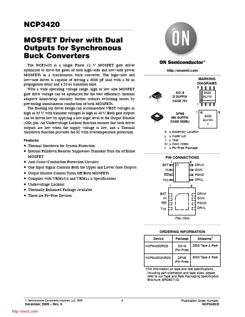
NCP3420MOSFET Driver with Dual Outputs for Synchronous Buck ConvertersThe NCP3420 is a single Phase 12 V MOSFET gate driver optimized to drive the gates of both high−side and low−side power MOSFETs in a synchronous buck converter. The high−side and low−side driver is capable of driving a 3000 pF load with a 30 ns propagation delay and a 20 ns transition time.With a wide operating voltage range, high or low side MOSFETgate drive voltage can be optimized for the best efficiency. Internal adaptive nonoverlap circuitry further reduces switching losses by preventing simultaneous conduction of both MOSFETs.The floating top driver design can accommodate VBST voltages as high as 35 V, with transient voltages as high as 40 V. Both gate outputs can be driven low by applying a low logic level to the Output Disable (OD) pin. An Undervoltage Lockout function ensures that both driver outputs are low when the supply voltage is low, and a Thermal Shutdown function provides the IC with overtemperature protection. Features•Thermal Shutdown for System Protection•Internal Pulldown Resistor Suppresses Transient Turn On of Either MOSFET•Anti Cross−Conduction Protection Circuitry•One Input Signal Controls Both the Upper and Lower Gate Outputs •Output Disable Control Turns Off Both MOSFETs •Complies with VRM10.x and VRM11.x Specifications •Undervoltage Lockout•Thermally Enhanced Package Available•These are Pb−Free DevicesDevice Package Shipping†ORDERING INFORMATIONSO−8(Pb−Free)2500 Tape & Reel NCP3420DR2GA= Assembly LocationL= Wafer LotY= YearW= Work WeekG= Pb−Free PackageMARKINGDIAGRAMSPIN CONNECTIONSSO−8D SUFFIXCASE 751DRVLPGNDSWNDRVH†For information on tape and reel specifications, including part orientation and tape sizes, please refer to our Tape and Reel Packaging Specification Brochure, BRD8011/D.DFN8MN SUFFIXCASE 506BJDFN8(Pb−Free)3000 Tape & Reel NCP3420MNR2GDRVLV CCPGNDODSWNINDRVHBST(Top View)3420ALYW GG18Figure 1. Block DiagramV CC DRVH BSTSWNDRVL PGNDODINPIN DESCRIPTIONSO −8DFN8Symbol Description11BSTUpper MOSFET Floating Bootstrap Supply. A capacitor connected between BST and SW pins holds this bootstrap voltage for the high −side MOSFET as it is switched. The recommended capacitor value is between 100 nF and 1.0 m F. An external diode is required with the NCP3420.22IN Logic −Level Input. This pin has primary control of the drive outputs.33OD Output Disable. When low, normal operation is disabled forcing DRVH and DRVL low.44V CC Input Supply. A 1.0 m F ceramic capacitor should be connected from this pin to PGND.55DRVL Output drive for the lower MOSFET.66PGND Power Ground. Should be closely connected to the source of the lower MOSFET.77SWN Switch Node. Connect to the source of the upper MOSFET.88DRVHOutput drive for the upper MOSFET.MAXIMUM RATINGSRating Value Unit Operating Ambient Temperature, T A0 to 85°C Operating Junction Temperature, T J (Note 1)0 to 150°CPackage Thermal Resistance: SO−8Junction−to−Case, R q JCJunction−to−Ambient, R q JA (2−Layer Board) Package Thermal Resistance: DFN8 (Note 2) Junction−to−Case, R q JC (From die to exposed pad) Junction−to−Ambient, R q JA 451237.555°C/W°C/W°C/W°C/WStorage Temperature Range, T S−65 to 150°C Lead Temperature Soldering (10 sec): Reflow (SMD styles only)Pb−Free (Note 3)260 peak°C JEDEC Moisture Sensitivity Level SO−8 (260 peak profile)1−Stresses exceeding Maximum Ratings may damage the device. Maximum Ratings are stress ratings only. Functional operation above the Recommended Operating Conditions is not implied. Extended exposure to stresses above the Recommended Operating Conditions may affect device reliability.1.Internally limited by thermal shutdown, 150°C min.2. 2 layer board, 1 in2 Cu, 1 oz thickness.3.60−180 seconds minimum above 237°C.NOTE:This device is ESD sensitive. Use standard ESD precautions when handling.MAXIMUM RATINGSPin Symbol Pin Name V MAX V MIN V CC Main Supply Voltage Input15 V−0.3 VPGND Ground0 V0 VBST Bootstrap Supply Voltage Input35 V wrt/PGND40 V v 50 ns wrt/PGND15 V wrt/SW−0.3 V wrt/SWSW Switching Node(Bootstrap Supply Return)35 V DC40 V < 50 ns−5.0 V DC−10 V < 200 nsDRVH High−Side Driver Output BST + 0.3 V35 V v 50 ns wrt/PGND15 V wrt/SW−0.3 V wrt/SW−2.0 V < 200 ns wrt/SWDRVL Low−Side Driver Output V CC + 0.3 V−0.3 V DC−5.0 V < 200 ns IN DRVH and DRVL Control Input 6.5 V−0.3 VOD Output Disable 6.5 V−0.3 V NOTE:All voltages are with respect to PGND except where noted.ELECTRICAL CHARACTERISTICS (Note 4)(V CC = 12 V, T A = 0°C to +85°C, T J = 0°C to +125°C unless otherwise noted.) Characteristic Symbol Condition Min Typ Max Unit SupplySupply Voltage Range V CC− 4.6−13.2V Supply Current I SYS BST = 12 V, IN = 0 V−0.7 6.0mA OD InputInput Voltage High V OD_HI− 2.0−−V Input Voltage Low V OD_LO−−−0.8V Hysteresis−−−400−mV Input Current−No internal pull−up or pull−down resistors−1.0−+1.0m APropagation Delay Time t pdlODt pdhOD − 1.01.025254545nsnsPWM InputInput Voltage High V PWM_HI− 2.0−−V Input Voltage Low V PWM_LO−−−0.8V Hysteresis−−−500−mV Input Current−No internal pull−up or pull−down resistors−1.0−+1.0m A High−Side DriverOutput Resistance, Sourcing Current−V BST− V SW = 12 V (Note 6)− 1.8 3.0W Output Resistance, Sinking Current−V BST− V SW = 12 V (Note 6)− 1.0 2.5W SW Pulldown Resitance−SW to PGND10−55k W Output Resistance, Unbiased−BST−SW = 0 V10−55k WTransition Times t rDRVHt fDRVH V BST− V SW = 12 V, C LOAD = 3.0 nF(See Figure 3)−−16113025nsnsPropagation Delay (Note 5)t pdhDRVHt pdlDRVH V BST− V SW = 12 V, C LOAD = 3.0 nF(See Figure 3)201030304545nsnsLow−Side DriverOutput Resistance, Sourcing Current−V CC = 12 V (Note 6)− 1.8 3.0W Output Resistance, Sinking Current−V CC− PGND = 12 V (Note 6)− 1.0 2.5W Output Resistance, Unbiased−V CC = PGND10−55k W Timeout Delay−DRVH−SW = 0−85−nsTransition Times t rDRVLt fDRVL V BST− V SW = 12 V, C LOAD = 3.0 nF(See Figure 3)−−16113025nsnsPropagation Delay (Note 5)t pdhDRVLt pdlDRVLV BST− V SW = 12 V, C LOAD = 3.0 nF(Note 6, t pdhDRVL Only) (See Figure 3)151030304545nsnsUndervoltage LockoutUVLO Startup−− 3.9 4.3 4.5V UVLO Shutdown−− 3.7 4.1 4.3V Hysteresis−−0.10.20.4V Thermal ShutdownOver Temperature Protection−(Note 6)150170−°C Hysteresis(Note 6)−20−°C 4.All limits at temperature extremes are guaranteed via correlation using standard Statistical Quality Control (SQC).5.For propagation delays, “t pdh’’ refers to the specified signal going high; “t pdl’’ refers to it going low.6.GBD: Guaranteed by design; not tested in production.Specifications subject to change without notice.Figure 2. Output Disable Timing DiagramDRVH or DRVLODFigure 3. Nonoverlap Timing DiagramDRVLDRVH −SWSWINAPPLICATIONS INFORMATIONTheory of OperationThe NCP3420 are single phase MOSFET drivers designed for driving two N−channel MOSFETs in a synchronous buck converter topology. The NCP3420 will operate from 5 V or 12 V, but have been optimized for high current multi−phase buck regulators that convert 12 V rail directly to the core voltage required by complex logic chips. A single PWM input signal is all that is required to properly drive the high−side and the low−side MOSFETs. Each driver is capable of driving a 3.3 nF load at frequencies up to 1 MHz.Low−Side DriverThe low−side driver is designed to drive a ground−referenced low R DS(on) N−Channel MOSFET. The voltage rail for the low−side driver is internally connected to the V CC supply and PGND.High−Side DriverThe high−side driver is designed to drive a floating low R DS(on) N−channel MOSFET. The gate voltage for the high side driver is developed by a bootstrap circuit referenced to Switch Node (SW) pin.The bootstrap circuit is comprised of an external diode, and an external bootstrap capacitor. When the NCP3420 are starting up, the SW pin is at ground, so the bootstrap capacitor will charge up to V CC through the bootstrap diode See Figure 4. When the PWM input goes high, the high−side driver will begin to turn on the high−side MOSFET using the stored charge of the bootstrap capacitor. As the high−side MOSFET turns on, the SW pin will rise. When the high−side MOSFET is fully on, the switch node will be at 12 V, and the BST pin will be at 12 V plus the charge of the bootstrap capacitor (approaching 24 V).The bootstrap capacitor is recharged when the switch node goes low during the next cycle.Safety Timer and Overlap Protection CircuitIt is very important that MOSFETs in a synchronous buck regulator do not both conduct at the same time. Excessive shoot−through or cross conduction can damage the MOSFETs, and even a small amount of cross conduction will cause a decrease in the power conversion efficiency. The NCP3420 prevent cross conduction by monitoring the status of the external mosfets and applying the appropriate amount of “dead−time” or the time between the turn off of one MOSFET and the turn on of the other MOSFET.When the PWM input pin goes high, DRVL will go low after a propagation delay (tpdlDRVL). The time it takes for the low−side MOSFET to turn off (tfDRVL) is dependent on the total charge on the low−side MOSFET gate. The NCP3420 monitor the gate voltage of both MOSFETs and the switchnode voltage to determine the conduction status of the MOSFETs. Once the low−side MOSFET is turned off an internal timer will delay (tpdhDRVH) the turn on of the high−side MOSFETLikewise, when the PWM input pin goes low, DRVH will go low after the propagation delay (tpdDRVH). The time to turn off the high−side MOSFET (tfDRVH) is dependent on the total gate charge of the high−side MOSFET. A timer will be triggered once the high−side mosfet has stopped conducting, to delay (tpdhDRVL) the turn on of the low−side MOSFETPower Supply DecouplingThe NCP3420 can source and sink relatively large currents to the gate pins of the external MOSFETs. In order to maintain a constant and stable supply voltage (V CC) a low ESR capacitor should be placed near the power and ground pins. A 1 m F to 4.7 m F multi layer ceramic capacitor (MLCC) is usually sufficient.Input PinsThe PWM input and the Output Disable pins of the NCP3420 have internal protection for Electro Static Discharge (ESD), but in normal operation they present a relatively high input impedance. If the PWM controller does not have internal pull−down resistors, they should be added externally to ensure that the driver outputs do not go high before the controller has reached its under voltage lockout threshold. The NCP5381 controller does include a passive internal pull−down resistor on the drive−on output pin. Bootstrap CircuitThe bootstrap circuit uses a charge storage capacitor (C BST) and the internal (or an external) diode. Selection of these components can be done after the high−side MOSFET has been chosen. The bootstrap capacitor must have a voltage rating that is able to withstand twice the maximum supply voltage. A minimum 50 V rating is recommended. The capacitance is determined using the following equation:C BST+Q GATED V BSTwhere Q GATE is the total gate charge of the high−side MOSFET, and D V BST is the voltage droop allowed on the high−side MOSFET drive. For example, a NTD60N03 has a total gate charge of about 30 nC. For an allowed droop of 300 mV, the required bootstrap capacitance is 100 nF. A good quality ceramic capacitor should be used.The bootstrap diode must be rated to withstand the maximum supply voltage plus any peak ringing voltages that may be present on SW. The average forward current can be estimated by:I F(AVG)+Q GATE f MAXwhere f MAX is the maximum switching frequency of the controller. The peak surge current rating should be checked in−circuit, since this is dependent on the source impedance of the 12 V supply and the ESR of C BST.Output EnablePWM inFigure 4. NCP3420 Example CircuitDFN8 3x3, 0.5PCASE 506BJ−01ISSUE O*For additional information on our Pb−Free strategy and solderingdetails, please download the ON Semiconductor Soldering andMounting Techniques Reference Manual, SOLDERRM/D.SOLDERMASK DEFINEDNOTES:1.DIMENSIONS AND TOLERANCING PER ASMEY14.5M, 1994.2.CONTROLLING DIMENSION: MILLIMETERS.3.DIMENSION b APPLIES TO PLATED TERMINALAND IS MEASURED BETWEEN 0.15 AND 0.30MM FROM TERMINAL.4.COPLANARITY APPLIES TO THE EXPOSEDPAD AS WELL AS THE TERMINALS.8X8XDIM MIN MAXMILLIMETERSA0.80 1.00A10.000.05A30.20 REFb0.180.30D 3.00 BSCD2 1.64 1.84E 3.00 BSCE2 1.35 1.55e0.50 BSCK0.20−−−L0.300.50DETAIL AOPTIONALCONSTRUCTIONDETAIL ADETAIL BLOPTIONALCONSTRUCTIONOPTIONALCONSTRUCTIONL10.000.03DIMENSION: MILLIMETERSMOUNTING FOOTPRINTSOIC −8D SUFFIX CASE 751−07ISSUE AJ0.6ǒmm inchesǓSCALE 6:1*For additional information on our Pb −Free strategy and solderingdetails, please download the ON Semiconductor Soldering and Mounting Techniques Reference Manual, SOLDERRM/D.SOLDERING FOOTPRINT*NOTES:1.DIMENSIONING AND TOLERANCING PER ANSI Y14.5M, 1982.2.CONTROLLING DIMENSION: MILLIMETER.3.DIMENSION A AND B DO NOT INCLUDE MOLD PROTRUSION.4.MAXIMUM MOLD PROTRUSION 0.15 (0.006)PER SIDE.5.DIMENSION D DOES NOT INCLUDE DAMBAR PROTRUSION. ALLOWABLE DAMBARPROTRUSION SHALL BE 0.127 (0.005) TOTAL IN EXCESS OF THE D DIMENSION AT MAXIMUM MATERIAL CONDITION.6.751−01 THRU 751−06 ARE OBSOLETE. NEW STANDARD IS 751−07.DIM A MIN MAX MIN MAX INCHES4.805.000.1890.197MILLIMETERS B 3.80 4.000.1500.157C 1.35 1.750.0530.069D 0.330.510.0130.020G 1.27 BSC 0.050 BSC H 0.100.250.0040.010J 0.190.250.0070.010K 0.40 1.270.0160.050M 0 8 0 8 N 0.250.500.0100.020S5.806.200.2280.244MYM0.25 (0.010)YM0.25 (0.010)Z SXS____ON Semiconductor and are registered trademarks of Semiconductor Components Industries, LLC (SCILLC). SCILLC reserves the right to make changes without further notice to any products herein. SCILLC makes no warranty, representation or guarantee regarding the suitability of its products for any particular purpose, nor does SCILLC assume any liability arising out of the application or use of any product or circuit, and specifically disclaims any and all liability, including without limitation special, consequential or incidental damages.“Typical” parameters which may be provided in SCILLC data sheets and/or specifications can and do vary in different applications and actual performance may vary over time. All operating parameters, including “Typicals” must be validated for each customer application by customer’s technical experts. SCILLC does not convey any license under its patent rights nor the rights of others. SCILLC products are not designed, intended, or authorized for use as components in systems intended for surgical implant into the body, or other applications intended to support or sustain life, or for any other application in which the failure of the SCILLC product could create a situation where personal injury or death may occur. Should Buyer purchase or use SCILLC products for any such unintended or unauthorized application, Buyer shall indemnify and hold SCILLC and its officers, employees, subsidiaries, affiliates,and distributors harmless against all claims, costs, damages, and expenses, and reasonable attorney fees arising out of, directly or indirectly, any claim of personal injury or death associated with such unintended or unauthorized use, even if such claim alleges that SCILLC was negligent regarding the design or manufacture of the part. SCILLC is an Equal Opportunity/Affirmative Action Employer. This literature is subject to all applicable copyright laws and is not for resale in any manner.PUBLICATION ORDERING INFORMATION分销商库存信息:ONSEMINCP3420DR2G NCP3420MNR2G。
123456789A B C D E F G H I J K L M N O P Q R S T U V W123456789A B C D E F G H I JK L M N O P Q R STUV WREV/ISS AMENDMENTS DATE APVD D.O.CHKD DRAWN TAIT ELECTRONICS2.SC.12T2000-200 MID-BAND MOBILE RADIOWITH DUAL-BAND OPTION120211A 220-01202-1115/06/98A T2000RPS 5AMODS TO NOISE-BLANKER & CHANGED BBY40 DIODES TO BB249J.F.J.F.M.L.18/9/926A ADDED NOISE-BLANKER. ADDED R420A & R421A.J.F.J.F.M.L.28/10/926B CHANGED NOISE BLANKER VARIANTS.J.F.J.F.M.L.26/11/92LOCK=5V UNLOCK=0VRX-FREQ66MHZ 88MHZCONTROL-VOLTS3V77V0FREQ66MHZ 88MHZTYP:********************7A MODS TO IMPROVE MANUFACTURABILITY.MC KB DEMB 24/7/93RX=4V2TX=5V97DCAD-WANG.MC8A ADDED PROGRAMMABLE BAND-WIDTH CCTRY.J.F.J.F.29/8/94TX=0V7RX=0VTYP:***********************1V.P-P.TYP @.60%-MOD’CONTROL-VOLTSTX4V610V66V.P-P.MAXRX7V414V0RX-FREQ66MHZ 88MHZTX:12V0CNTRL-VOLTS5V812V8’*BANDNARROW MID WIDE DUAL-BAND*R133---3K9S*R135---220KS*R139---10KS*R1513K3S 3K3S 3K3S’1K5S*R152390KS 390KS 390KS 220KS*R154---22KS*R1620S 0S 0S 18KS*R1630S 0S 0S 3K3STX:8V0*R164---470KS*R165---560KS*R166---22KS*R167---10KS*R168---6K8S*R170---2K2S*R1940S 0S 0S 390KS*C120---47UFI16A*C189470PS 470PS 470PS 150PS*C190470PS 470PS 470PS 150PS0V.AT.REST9A CREATED A VARIANT TABLE FOR DUAL BAND.YH 25/5/95*Q119---BC848*Q118---BC848*Q117---BC848*Q116---BFR3110A ADDED CAPS FOR EMCDBH 8V0.AT.RESTTYP:3V1.DC @-70DBM.INPUT11A DIODE,COPPER,FUSE UPDATES RPS 27/05/98*C12047U*C189470P*C190470PDS G *Q116BFR31*Q117BC848*Q118BC848*Q119BC848*R1333K9*R135220K*R13910K*R1513K3*R152390K*R15422K*R1620 *R1630 *R164470K*R165560K*R16622K*R16710K *R1686K8*R1702K2*R1940C11N0C10010NC10156P C102180PC10310NC104100NC10510PC1061N0C107100PC1081N0C10927PC110270PC1111N0C11233PC113270PC1141N0C11527P C1161N0C121100PC1221N0C12310NC12422PC12512PC12622P C12739PC12810NC12910NC13010NC13439PC135180PC1365P6 C137180PC13810NC14010NC14139PC14210NC145100PC146270PC14710NC14847PC14910NC150100P C151100NC152100PC152A 10NC1534U7C153A 100PC15410NC155100PC1560C157100NC15810N C17447UC175100NC176100NC17910NC18047NC18147NC18510N C18610NC1871N0C188100PC1911N0 C19233PC1934U7C1941N0C1951N0C197100NC198220PC1991N0C21N0C20010NC2011N0 C20247UC2034U7C2051N0C206100NC20710NC21347UC2141N0C2154U7C21610NC21747UC2184U7C21947UC22015NC2211U0 C222100NC2231N0C2241N0C2251N0C2261P8C2271N0 C2281N0C22947UC23010NC2314P7C23215PC2344U7C23910NC2401N0C24110NC2431N0C24518PC24610NC24810NC25718P C31N0C3004U7 C3011N0C30227PC303100N C3041N0C305120PC306120PC307100NC308100NC3091N0C3104N7C31147PC312120PC313680PC3151N0 C3161N0C3171N0C3181N0C319100N C3201N0C321100NC32247PC323270PC325680PC32647N C327680PC3281N0C329150P C330120P C33356PC33439PC33668P C3371N0C33822PC33922P C34056PC34182PC34210PC3432N2C34447P C3451N0C34615P C34727PC3481N0C3491N0C35082PC3531N0C3561N0C357100NC360150PC403470PC 4104U 7C411100NC41247U C413100NC414470UC4151000UC4161N0 C419100NC420100NC42356UC4244U7C4254U7C4264N7C4274U7C4284U7C4291N0C43056UC4511N0C4551N0D118VD10112D101A BB419 12D10212D102A BB419 12D10312D103A BB419 12BAT17DSD11031 BAT17DS D11023BAT17DS D11123BAT17DS D11131BAT18D140A 23 BAV99D20023BAV99D20031 BAV70D20223D203BB41912D204BB419 12D205BB41912D206BB419 12BAT18D20823 BAT18D20923D3011SS97D303UM9401 D304UM9401 D305BA482 BAV70D40113BAV70D40123ININ OUT PD OUTRVSYNTHESISERIC201145158-2F 8DATA 10CLK9EN11GND6F 13F 3OSC 1OSC 2REF 14MC 12+V 4LD 7OUT5PR 16PV 15DIVIDERMC12016IC203IN5BP 6MOD 1GND4VCC 8REG 7VCC22OUT3VREGIC4037808ACT VIN1GND2VOUT 3VREGIC4047805ACT VIN1GND2VOUT 3L1#4S3BL1018.5T/4.5L104#669L105#669L106#669L107RF BALUN32146L108RF BALUN32146L10968NH L114#662L116#662L119#655 23614L120M21BL200M21B L2053U3L206#1009L2073U3L2085.5T/4.0L2108.5T/4.0L300L3015.5T/3.0 L3023.5T/4.5L3033U3L3042.5T/3.5 L3058.5T/3.0L306M21BL3073.5T/2.5 L308L309#4S3BL3103.5T/4.0L3112.5T/3.0L312330NHL3137.5T/3.0 L3148.5T/4.5 L315#18 (3B BEAD)L3163.5T/4.0L317#18 (3B BEAD)L3182.5T/3.0L3193U3L3205.5T/4.0 L3218.5T/4.5 L3224.5T/4.5L3235.5T/3.0 L324#18 (3B BEAD)L3251.5T/3.0L3268.5T/4.5L3271.5T/2.5L3285.5T/3.5 L3291.5T/3.5L3303.5T/2.5L331M21BL3321.5T/2.0L401#650 23614PAD-1D SG Q100BFR31Q101951 Q102BC857Q103951Q104BSS83GD B S Q105951Q106BC848Q107BFS17 Q108BFS17 Q109BF824Q115BC848Q203BC848Q204BC848Q205BC857Q206BC848Q207BC857Q208BC848Q209BC857DS G Q210BFR31D S G Q212BF512Q213BC848Q214BFS17Q215BFS17Q301951Q302MRF386667142358Q303BC848Q304BD234Q305BFQ43 Q306MRF1946AQ307BC807Q308BC807Q309BC848Q401BC857Q402BC817CWRV15347K231CW RV22247K 231CWRV324470K231R100470 R1013K9R102560R1032K2R10482R10518R106100KR107100KR108100KR1090 R1101M0R1111M0R11218R1134R7 R114820R11512KR1164R7R11710R118100R11910R120820R121180R122100KR123100K R124100K R12510K R12610KR12710KR128150R12947R131270R132150R13410R1364R7R1374R7R138100KR14068KR140A 33KR1411K5R14227KR142A 100KR14333KR143A 33KR14468K R144A 120KR1451K5R145A 33K R14622 R147220 R148560 R1490805 R150100KR1531K0R155100KR156100R15710KR1581K0R15947R16010R1611K0R19568KR196100R197100R1982K2R199100R2133K9R2141K8R2153K9R21647R21747R22322KR2248K2R22522K R2268K2R2278K2R2283K3R22922R230390 R231180R2322K2R233680R234270R235330 R23647R237100R2388K2R23922K R240100KR2411K8R24222R2432K2R24422R24522R246100R24747R248100KR24910R2502K2R251150R2521K2R253680R25422 R25510 R2561K8R25710 R259270R26027R26110R26910 R27010R271180R272180R27310R2743K9R27510R278100KR28410KR28539K R28615K R28782KR288120K R30068 R301330R3021K0R3031K0R30447R30510 R30610R307470R30810 R308A10 R30910 R31010R311820R312680 R313180R31410R31518R31622R3171R0 R317A 1R0 R317B 1R0 R317C1R0R318180 R319180R32015KR321390 R321A 390 R32210R32310 R32510 R326220KR3271K0 R328150R32947KR330220KR332100R3332K2R33456KR33510KR336220R3370 R338680R339270KR340220K R341220R3421K8R35010 R418680R42039K R420A 3K3R42139KR421A 3K3 R42222R4251K0R4264R7R4274R7R42822R42927KR4306K8R431100KR43210R433100R43447R4371K0S4IC1013371D 1011OUT IN IC1013371DLIM 5GND 15VCC 4DEC 6DEC 7QUAD 8AF 9RSSI13IC1013371D1214+-IC20233078D321+-IC20233078D567+-IC20434002D321+-IC20434002D 5671020IC402+6GND 9SUB1SB 5VCC3BS 4O/P2#D203BB43912#D204BB43912#D205BB43912#D206BB43912BAV70D20213C354NPOLY#D103BB43912#D102BB43912#D101BB43912#D101A BB439 12#D102A BB439 12#D103A BB439 12P1+5V15P1+8V10P1+8V-SYNTH9P1AF-SIG8P1BUSY3P1CLK 12P1DATA 13P1DET-AF5P1ENABLE14P1GND4P1GND16P1GND1P1LCK-DET11P1LF-SIG6P1MOD 7P1RSSI2P2+13.8V 8P2+13.8V-US6P2+13V-ECON 5P2+5-VOLTS7P2+8V-OUT 9P2+8VTX 10P2AUDIO-PA1P2EXTRNL3P2GND2P2IGN4P2PWR-CNTRL12P2PWR-SENSE 11P3AUDIO4P3EXTRNL 1P3GND 5P3GND 3P3IGN 7P3SPKR 2P313.8V-UNSW6P5+8VOLTS 7P5AF-OUT 10P5CMPRTR-OUT6P5DETECT-AUDIO8P5FILTER3P5GND2P5MIXER4P5NSE-DET5P5QUAD-COIL1P5455-OUT9P6+8V-SYNTH10P6+8V-SYNTH4P6AF-SIG 9P6GND3P6GND2P6LF-SIG 7P6MOD 6P6REF-MOD5P6TCXO 1P6TX-AF8P7INT 2P7SPKR 1+13.8V+13.8V+13.8V-UNSW+13.8V-UNSW+13.8V-UNSW+13V-ECON+13V-ECON +30V+30V+5-VOLTS +5-VOLTS+5V+5V+5V+8-VOLTS+8-VOLTS+8-VOLTS+8-VOLTS+8-VOLTS+8-VOLTS+8-VOLTS+8V+8V+8V+8V+8V+8V-OUT+8V-OUT +8V-SYNTH+8V-SYNTH+8V-SYNTH+8V-SYNTHSYNTHESISERNOISE BLANKERTCXO84DELAY LINE+8V-TXRX-TUNE VOLTAGE1ST MIXERPDL16MPDL12M P1 TO CONTROL PCBP2 TO CNTRL PCBPRESCALER32161PIN SWITCHTO LOOM CONNECTOR P2PIN-7REF-MOD ADJCOUPLERTO CNTRL-PCB ONLY, VIA P2 PIN-9(FROM +8V REGULATOR)P R I N T E DPWR-CNTRLUNDER-WALL DECOUPLING4S34S34S34S34S3***DUAL SMALL 4S3 BEADSL300, L308, L309*RF-PALOOP FILTER+8V TX DELAYEDTO LOOP-FILTER IC202, PIN-887AUDIO PA(VIA R1)TO LOOM CONNECTOR P2 PIN-6& RF POWER-AMPTRACK-FUSEPCB-GND INTERNAL SPKRPL2USPKRGNDSK7HMCHC U T F O R E X T R N L S P K RGNDFROM CNTRL PCB +13.8V-ECONOMY VIA P2-PIN 5IF PCB(IPN:220-01384-XX)(IPN:220-01201-XX)FROM +8V REGULATOR ON CNTRL-PCB, VIA P1 PIN-948TX-AUDIO PCB(IPN:220-01389-XX)&AMENDMENTS DRAWN CHKD D.O.APVD DATEREV/ISS 1V87V087V143V40V76V27V85V754V04V04V54V04V02V70V64V5C322C323C325C326Q306R315R31945L J 211109816D C G AH 3E KF 7B TAIT ELECTRONICST2000-200 PCB LAYOUT - BOTTOM SIDEIPN:ISS:ID:DATE:220-01202-1111B2.BA 9 Jul 1998SMD BOT SLOT 200 5325SMD BOT REF HOLE 5100 5325IPN 220-01202-11 ISS: B REPEAT DATA 1 0 1 0SMD TOP SLOT 4900 5325SMD TOP REF HOLE 0 5325T2000-200 MAIN BOARD#D 101#D 102#D 102A#D 103#D 103A#D203#D204#D205#D206*C120*C 189*C190*Q116*Q 117*Q118*Q119*R 133*R135*R139*R151*R152*R154*R 162*R163*R 164*R165*R166*R167*R168*R170*R194C1C100C 101C102C103C104C 105C106C 107C 108C109C110C 111C112C113C 114C115C116C121C 122C123C124C125C126C 127C128C129C 130C134C 135C136C 137C 138C140C141C142C145C 146C 147C148C 149C150C151C152C 152AC153C 153AC 154C155C156C157C158C 175C176C179C180C181C185C186C 187C 188C191C 192C193C194C195C197C198C199C2C 200C201C202C203C 205C206C 207C214C215C 216C217C218C219C220C221C222C 223C224C225C226C 227C228C229C230C 231C 232C234C239C240C241C 243C245C 246C248C257C3C300C301C302C 303C304C305C 306C 307C 308C309C310C311C312C313C 315C 316C317C 318C 319C320C321C327C 328C329C330C333C334C336C 337C338C339C340C341C 342C 343C344C345C 346C 347C 348C 349C350C 353C354C 356C 357C 360C 403C410C 411C412C 413C414C415C 416C 419C 420C423C424C425C426C427C428C429C430C 451C455D1D110D111D140AD200D202D208D209D 301D 303D 304D401IC101IC201IC202IC203IC204I C 402I C 403L101L104L105L106L107L108L109L114L116L119L120L 200L 205L206L207L208L210L 300L301L302L303L 304L305L306L307L308L 310L311L313L314L315L 316L317L 318L319L320L321L 322L323L324L325L326L327L328L330L331L332L401P1P2P3P5P6P7PAD-1Q100Q101Q102Q103Q104Q105Q106Q107Q108Q109Q115Q203Q204Q205Q206Q207Q208Q209Q210Q212Q213Q214Q215Q301Q302Q303Q 304Q305Q307Q308Q309Q401Q402R 100R101R102R103R104R105R106R 107R108R109R 110R 111R 112R 113R 114R115R 116R 117R 118R119R120R121R 122R 123R124R125R 126R127R128R129R 131R132R 134R136R137R138R140R 140AR 141R 142R142AR 143R 143AR144R144AR145R145AR146R147R148R 149R150R 153R 155R 156R 157R 158R159R160R 161R195R196R197R 198R199R213R214R215R 216R 217R 223R224R225R226R227R228R229R230R231R232R233R 234R235R236R 237R238R239R240R241R 242R 243R244R245R 246R 247R248R 249R250R251R 252R 253R254R255R256R257R 259R 260R261R269R270R271R272R273R274R275R278R284R285R286R 287R 288R 300R301R 302R303R304R305R306R307R 308R 308AR 309R 310R311R312R313R 314R 316R 318R320R 321R 321AR 322R 326R327R 328R329R 330R332R333R 334R 335R 336R337R 338R 339R 340R 341R 342R418R420R 420AR 421R 421AR 422R 425R426R427R 428R429R430R 431R432R 433R434R 437RV153RV222RV324S4TOPFIDA11085H73EB 6D 11GLC 942FJ K A TAIT ELECTRONICST2000-200 PCB LAYOUT - TOP SIDEIPN:ISS:ID:DATE:220-01202-1111B 1.TA 9 Jul 1998H /S I N KD203D204D205D206TOPFIDBR317A R317BR317R317CSHIELDD 101AD 101#D 101AD 102A D 102D 103A D 103L1R323L309R 325R 350D 305L329I C 404L 312C213C1740123456789123456789AB C D E F G H J K L M N P Q RREV/ISS AMENDMENTS DATEAPVD D.O.CHKD DRAWN NO.SHEETS:FILE NAME:TAIT ELECTRONICSIPN:FILE DATE:ISSUE:ID:.2.SC.PROJECT:DESIGNER:22T2000-200 MID-BAND MOBILE RADIO POWER PINS, CONNECTORS ETC.120211A 220-01202-1115/06/98A T2000RPS H/SINKA4M2524 HEATSINKIC20233078D V-4V+8IC20434002D V-4V+8P116 WAY PADDLE CONNECTORP212 WAY PADDLE CONNECTORP37WAY SIDE ENTRY SKTP52X5 WAY TOP ENTRY PLUGP62X5 WAY TOP ENTRY PLUGP72 WAY PLUGSHIELDA3M2594 RX SHIELDTOPFIDA FIDUCIALTOPFIDB FIDUCIALMIXEROSCIC1013371DIN16IN 1OUT2OUT3+1020IC40287+8-VOLTSNOT334NOT567NOT867NOT965。
元器件交易网IMPORTANT NOTICETexas Instruments (TI) reserves the right to make changes to its products or to discontinue any semiconductorproduct or service without notice, and advises its customers to obtain the latest version of relevant informationto verify, before placing orders, that the information being relied on is current and complete.TI warrants performance of its semiconductor products and related software to the specifications applicable atthe time of sale in accordance with TI’s standard warranty. Testing and other quality control techniques areutilized to the extent TI deems necessary to support this warranty. Specific testing of all parameters of eachdevice is not necessarily performed, except those mandated by government requirements.Certain applications using semiconductor products may involve potential risks of death, personal injury, orsevere property or environmental damage (“Critical Applications”).TI SEMICONDUCTOR PRODUCTS ARE NOT DESIGNED, INTENDED, AUTHORIZED, OR WARRANTEDTO BE SUITABLE FOR USE IN LIFE-SUPPORT APPLICATIONS, DEVICES OR SYSTEMS OR OTHERCRITICAL APPLICATIONS.Inclusion of TI products in such applications is understood to be fully at the risk of the customer. Use of TIproducts in such applications requires the written approval of an appropriate TI officer. Questions concerningpotential risk applications should be directed to TI through a local SC sales office.In order to minimize risks associated with the customer’s applications, adequate design and operatingsafeguards should be provided by the customer to minimize inherent or procedural hazards.TI assumes no liability for applications assistance, customer product design, software performance, orinfringement of patents or services described herein. Nor does TI warrant or represent that any license, eitherexpress or implied, is granted under any patent right, copyright, mask work right, or other intellectual propertyright of TI covering or relating to any combination, machine, or process in which such semiconductor productsor services might be or are used.Copyright © 1998, Texas Instruments Incorporated。
8TMS320C6745,TMS320C6747SPRS377F –SEPTEMBER 2008–REVISED JUNE 2014Submit Documentation FeedbackProduct Folder Links:TMS320C6745TMS320C6747Device Overview Copyright ©2008–2014,Texas Instruments Incorporated3Device Overview3.1Device CharacteristicsTable 3-1provides an overview of the C6745/6747low power digital signal processor.The table shows significant features of the device,including the capacity of on-chip RAM,peripherals,and the package type with pin count.Table 3-1.Characteristics of the C6745/C6747ProcessorHARDWARE FEATURESC6745C6747PeripheralsNot all peripherals pinsare available at the same time (for moredetail,see the Device Configurations section).EMIFB16bit,up to 128MB SDRAM 16/32bit,up to 256MB SDRAM EMIFAAsynchronous (8-bit bus width)RAM,Flash,NOR,NAND Asynchronous (8/16-bit bus width)RAM,Flash,16bit up to 128MB SDRAM,NOR,NAND Flash Card InterfaceMMC and SD cards supported.EDMA332independent channels,8QDMA channels,2Transfer controllers Timers264-Bit General Purpose (each configurable as 2separate 32-bit timers,1configurable as Watch Dog)UART3(one with RTS and CTS flow control)SPI2(each with one hardware chip select)I 2C2(both Master/Slave)Multichannel AudioSerial Port [McASP]2(each with transmit/receive,FIFO buffer,16/9serializers)3(each with transmit/receive,FIFO buffer,16/9serializers)10/100Ethernet MAC with Management Data I/O 1(RMII Interface)eHRPWM 6Single Edge,6Dual Edge Symmetric,or 3Dual Edge Asymmetric Outputs eCAP 332-bit capture inputs or 332-bit auxiliary PWM outputs eQEP232-bit QEP channels with 4inputs/channel UHPI-1(16-bit multiplexed address/data)USB 2.0(USB0)Full Speed Host Or Device with On-Chip PHY High-Speed OTG Controller with on-chip OTG PHY USB 1.1(USB1)-Full-Speed OHCI (as host)with on-chip PHY General-PurposeInput/Output Port8banks of 16-bit LCD Controller-1RTC-1(32KHz oscillator and seperate power trail.Provides time and date tracking and alarm capability.)PRU Subsystem(PRUSS)2Programmable PRU Cores On-Chip Memory Size (Bytes)320KB RAM 448KB RAMOrganization DSP 32KB L1Program (L1P)/Cache (up to 32KB)32KB L1Data (L1D)/Cache (up to 32KB)256KB Unified Mapped RAM/Cache (L2)DSP Memories can be made accessible to EDMA3,and other peripherals.-ADDITIONAL MEMORY128KB RAMC674x CPU ID +CPU Rev ID Control Status Register (CSR.[31:16])0x1400C674x MegamoduleRevision Revision ID Register (MM_REVID[15:0])0x000051TMS320C6745,TMS320C6747SPRS377F –SEPTEMBER 2008–REVISED JUNE 2014Submit Documentation FeedbackProduct Folder Links:TMS320C6745TMS320C6747Device Overview Copyright ©2008–2014,Texas Instruments Incorporated Table 3-25.General Purpose Input Output Terminal Functions (continued)SIGNAL NAME PIN NOTYPE (1)PULL (2)MUXED DESCRIPTIONPTPZKB GP4USB0_DRVVBUS/GP4[15]-E4O IPD USB0GPIO Bank 4AMUTE1/EPWMTZ/GP4[14]132D4O IPD McASP1,eHRPWM0,eHRPWM1,eHRPWM2AFSR1/GP4[13]166L3I/O IPD McASP1ACLKR1/ECAP2/APWM2/GP4[12]165L2I/O IPD McASP1,eCAP2AHCLKR1/GP4[11]-L1I/O IPD McASP1AFSX1/EPWMSYNCI/EPWMSYNCO/GP4[10]163K4I/O IPD McASP1,eHRPWM0AXR1[9]/GP4[9]-M1I/O IPD McASP1AXR1[8]/EPWM1A/GP4[8]168M2I/O IPD McASP1,eHRPWM1A AXR1[7]/EPWM1B/GP4[7]169M3I/O IPD McASP1,eHRPWM1B AXR1[6]/EPWM2A/GP4[6]170M4I/O IPD McASP1,eHRPWM2A AXR1[5]/EPWM2B/GP4[5]171N1I/O IPD McASP1,eHRPWM2B AXR1[4]/EQEP1B/GP4[4]173N2I/O IPD McASP1,eQEP AXR1[3]/EQEP1A/GP4[3]174P1I/O IPD AXR1[2]/GP4[2]175P2I/O IPD McASP1AXR1[1]/GP4[1]176R2I/O IPD AXR1[0]/GP4[0]1T3I/O IPD GP5EMB_WE_DQM[0]/GP5[15]60K14O IPU EMIFB GPIOBank 5EMB_WE_DQM[1]/GP5[14]85C15O IPU SPI1_SCS[0]/UART2_TXD/GP5[13]8P4O IPU SPI1,UART2SPI1_ENA/UART2_RXD/GP5[12]7R4I IPU AXR1[11]/GP5[11]6T4I/O IPU McASP1AXR1[10]/GP5[10]4N3I/O IPU UART0_TXD/I2C0_SCL/TM64P0_OUT12/GP5[9]/BOOT[9]2R3I IPU UART0,I2C0,BOOT UART0_RXD/I2C0_SDA/TM64P0_IN12/GP5[8]/BOOT[8]3P3O IPU SPI1_CLK/EQEP1S/GP5[7]/BOOT[7]16T6I IPD SPI1,eQEP1,BOOT SPI1_SIMO[0]/I2C1_SDA/GP5[6]/BOOT[6]14N5I/O IPU SPI1,I2C1,BOOT SPI1_SOMI[0]/I2C1_SCL/GP5[5]/BOOT[5]13P5I/O IPU SPI0_SCS[0]/UART0_RTS/EQEP0B/GP5[4]/BOOT[4]9N4I IPU SPI0,UART0,eQEP0,BOOT SPI0_ENA/UART0_CTS/EQEP0A/GP5[3]/BOOT[3]12R5I IPU SPI0_CLK/EQEP1I/GP5[2]/BOOT[2]11T5I IPD SPI0,eQEP1,BOOT SPI0_SIMO[0]/EQEP0S/GP5[1]/BOOT[1]18P6I IPD SPI0,eQEP0,BOOT SPI0_SOMI[0]/EQEP0I/GP5[0]/BOOT[0]17R6I IPD。
LOGIC NETWORK452CAP–V SO–8D SUFFIX CASE 751PIN CONFIGURATION(Top View)12348765NC CAP +GND CAP –V +OSC LV V OUTON Semiconductor and are trademarks of Semiconductor Components Industries, LLC (SCILLC). SCILLC reserves the right to make changes without further notice to any products herein. SCILLC makes no warranty, representation or guarantee regarding the suitability of its products for any particular purpose, nor does SCILLC assume any liability arising out of the application or use of any product or circuit, and specifically disclaims any and all liability, including without limitation special, consequential or incidental damages. “Typical” parameters which may be provided in SCILLC data sheets and/or specifications can and do vary in different applications and actual performance may vary over time. All operating parameters, including “Typicals” must be validated for each customer application by customer’s technical experts. SCILLC does not convey any license under its patent rights nor the rights of others.SCILLC products are not designed, intended, or authorized for use as components in systems intended for surgical implant into the body, or other applications intended to support or sustain life, or for any other application in which the failure of the SCILLC product could create a situation where personal injury or death may occur. Should Buyer purchase or use SCILLC products for any such unintended or unauthorized application, Buyer shall indemnify and hold SCILLC and its officers, employees, subsidiaries, affiliates, and distributors harmless against all claims, costs, damages, and expenses, and reasonable attorney fees arising out of, directly or indirectly, any claim of personal injury or death associated with such unintended or unauthorized use, even if such claim alleges that SCILLC was negligent regarding the design or manufacture of the part. SCILLC is an Equal Opportunity/Affirmative Action Employer. PUBLICATION ORDERING INFORMATIONCENTRAL/SOUTH AMERICA:Spanish Phone:303–308–7143 (Mon–Fri 8:00am to 5:00pm MST)Email:ONlit–spanish@ASIA/PACIFIC: LDC for ON Semiconductor – Asia SupportPhone:303–675–2121 (Tue–Fri 9:00am to 1:00pm, Hong Kong Time)Toll Free from Hong Kong & Singapore:001–800–4422–3781Email: ONlit–asia@JAPAN: ON Semiconductor, Japan Customer Focus Center4–32–1 Nishi–Gotanda, Shinagawa–ku, Tokyo, Japan 141–8549Phone: 81–3–5740–2745Email: r14525@。