Fabrication, Characterization, and Analysis of a DRIE CMOS-MEMS Gyroscope
- 格式:pdf
- 大小:1.43 MB
- 文档页数:10

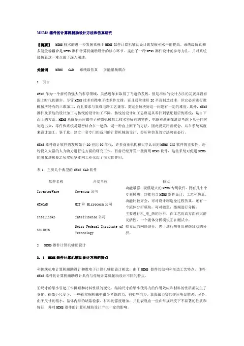
MEMS器件的计算机辅助设计方法和仿真研究【摘要】MEMS技术的进一步发展依赖于MEMS器件计算机辅助设计的发展和水平的提高。
系统级仿真和多能量场耦合是MEMS器件计算机辅助设计的核心环节。
提出了一种MEMS器件设计的参考方法,并对系统级仿真这一难点做了深入阐述。
关键词MEMS CAD 系统级仿真多能量场耦合1 引言MEMS作为一个新兴的强大的科学领域,虽然近年来取得了飞速的发展,但是相应的设计方法的发展却没有跟上时代的脚步。
尽管MEMS技术有微电子技术作支撑,而且通常使用IC平面制造技术,但它必须进行微机械所特有的三维加工,而且要求与集成电路工艺兼容,要完全解决好这一问题有一定的难度。
此外,MEMS 器件及系统的设计加工与传统的设计加工不同。
传统的设计加工思路是从零件到装配最后到系统,是自下而上的方法。
MEMS系统是采用微电子和微机械加工技术将所有的零件、电路和系统在通盘考虑下几乎同时制造出来,零件和系统是紧密结合在一起的,是一种自上而下的方法。
因此要采用新观念,站在系统高度来设计加工。
鉴于此,建立一套专门的适用的计算机辅助设计、分析和仿真的方法势在必行。
MEMS器件设计软件的发展始于2O世纪8O年代,许多商业机构和大学认识到MEMS CAD软件的重要性,纷纷投入大量的人力物力进行这方面的研究工作。
目前已经开发一些商用MEMS软件,这些系统对促进MEMS 的研究进展使之从实验室走向工业化起了很大的作用。
表1:主要几个典型的MEMS CAD软件软件名称开发单位特点CoventorWare Coventor公司功能最强、规模最大的MEMS专用软件,拥有几十个专业模块,功能包含MEMS器件设计、工艺和仿真。
MEMCAD MIT和 Microcosm公司功能比较齐全,可对设计制造全过程仿真。
还有一个流体分析模块,可对微泵,微阀进行分析。
IntelliCAD IntelliSense公司主要进行机_电_热的分析,在工艺仿真方面有大的灵活性,一个流体分析模块正在测试中。
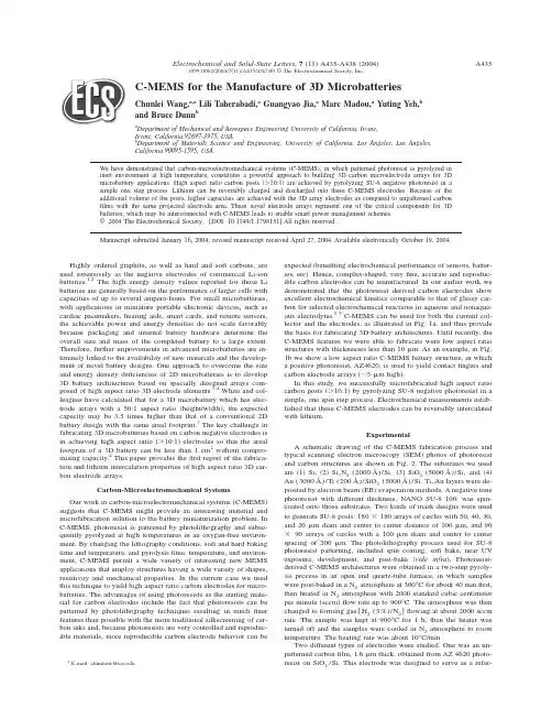
C-MEMS for the Manufacture of3D MicrobatteriesChunlei Wang,a,z Lili Taherabadi,a Guangyao Jia,a Marc Madou,a Yuting Yeh,band Bruce Dunn ba Department of Mechanical and Aerospace Engineering University of California,Irvine,Irvine,California92697-3975,USAb Department of Materials Science and Engineering,University of California,Los Angeles,Los Angeles,California90095-1595,USAWe have demonstrated that carbon-microelectromechanical systems͑C-MEMS͒,in which patterned photoresist is pyrolyzed in inert environment at high temperature,constitutes a powerful approach to building3D carbon microelectrode arrays for3D microbattery applications.High aspect ratio carbon posts͑Ͼ10:1͒are achieved by pyrolyzing SU-8negative photoresist in a simple one step process.Lithium can be reversibly charged and discharged into these C-MEMS electrodes.Because of the additional volume of the posts,higher capacities are achieved with the3D array electrodes as compared to unpatterned carbon films with the same projected electrode area.These novel electrode arrays represent one of the critical components for3D batteries,which may be interconnected with C-MEMS leads to enable smart power management schemes.©2004The Electrochemical Society.͓DOI:10.1149/1.1798151͔All rights reserved.Manuscript submitted January16,2004;revised manuscript received April27,2004.Available electronically October19,2004.Highly ordered graphite,as well as hard and soft carbons,are used extensively as the negative electrodes of commercial Li-ion batteries.1,2The high energy density values reported for these Li batteries are generally based on the performance of larger cells with capacities of up to several ampere-hours.For small microbatteries, with applications in miniature portable electronic devices,such as cardiac pacemakers,hearing aids,smart cards,and remote sensors, the achievable power and energy densities do not scale favorably because packaging and internal battery hardware determine the overall size and mass of the completed battery to a large extent. Therefore,further improvements in advanced microbatteries are in-timately linked to the availability of new materials and the develop-ment of novel battery designs.One approach to overcome the size and energy density deficiencies of2D microbatteries is to develop 3D battery architectures based on specially designed arrays com-posed of high aspect ratio3D electrode elements.3,4White and col-leagues have calculated that for a3D microbattery which has elec-trode arrays with a50:1aspect ratio͑height/width͒,the expected capacity may be3.5times higher than that of a conventional2D battery design with the same areal footprint.3The key challenge in fabricating3D microbatteries based on carbon negative electrodes is in achieving high aspect ratio͑Ͼ10:1͒electrodes so that the areal footprint of a3D battery can be less than1cm2without compro-mising capacity.4This paper provides thefirst report of the fabrica-tion and lithium intercalation properties of high aspect ratio3D car-bon electrode arrays.Carbon-Microelectromechanical Systems Our work in carbon-microelectromechanical systems͑C-MEMS͒suggests that C-MEMS might provide an interesting material and microfabrication solution to the battery miniaturization problem.In C-MEMS,photoresist is patterned by photolithography and subse-quently pyrolyzed at high temperatures in an oxygen-free environ-ment.By changing the lithography conditions,soft and hard baking time and temperature,and pyrolysis time,temperature,and environ-ment,C-MEMS permit a wide variety of interesting new MEMS applications that employ structures having a wide variety of shapes, resistivity and mechanical properties.In the current case we used this technique to yield high aspect ratio carbon electrodes for micro-batteries.The advantages of using photoresists as the starting mate-rial for carbon electrodes include the fact that photoresists can be patterned by photolithography techniques resulting in muchfiner features than possible with the more traditional silkscreening of car-bon inks and,because photoresists are very controlled and reproduc-ible materials,more reproducible carbon electrode behavior can be expected͑benefiting electrochemical performance of sensors,batter-ies,etc͒.Hence,complex-shaped,veryfine,accurate and reproduc-ible carbon electrodes can be manufactured.In our earlier work wedemonstrated that the photoresist derived carbon electrodes showexcellent electrochemical kinetics comparable to that of glassy car-bon for selected electrochemical reactions in aqueous and nonaque-ous electrolytes.5-7C-MEMS can be used for both the current col-lector and the electrodes,as illustrated in Fig.1a,and thus providethe basis for fabricating3D battery architectures.Until recently,theC-MEMS features we were able to fabricate were low aspect ratiostructures with thicknesses less than10m.As an example,in Fig.1b we show a low aspect ratio C-MEMS battery structure,in whicha positive photoresist,AZ4620,is used to yield contactfingers andcarbon electrode arrays͑ϳ5m high͒.In this study,we successfully microfabricated high aspect ratiocarbon posts͑Ͼ10:1͒by pyrolyzing SU-8negative photoresist in asimple,one spin step process.Electrochemical measurements estab-lished that these C-MEMS electrodes can be reversibly intercalatedwith lithium.ExperimentalA schematic drawing of the C-MEMS fabrication process andtypical scanning electron microscopy͑SEM͒photos of photoresistand carbon structures are shown in Fig.2.The substrates we used are͑1͒Si,͑2͒Si3N4(2000Å)/Si,͑3͒SiO2(5000Å)/Si,and͑4͒Au(3000Å)/Ti(200Å)/SiO2(5000Å)/Si.Ti,Au layers were de-posited by electron beam͑EB͒evaporation methods.A negative tonephotoresist with different thickness,NANO SU-8100,was spin-coated onto those substrates.Two kinds of mask designs were used to generate SU-8posts:180ϫ180arrays of circles with50,40,30, and20m diam and center to center distance of100m,and90ϫ90arrays of circles with a100m diam and center to center spacing of200m.The photolithography process used for SU-8photoresist patterning,included spin coating,soft bake,near UVexposure,development,and post-bake͑vide infra͒.Photoresist-derived C-MEMS architectures were obtained in a two-step pyroly-sis process in an open end quartz-tube furnace,in which samples were post-baked in a N2atmosphere at300°C for about40minfirst, then heated in N2atmosphere with2000standard cubic centimeter per minute͑sccm͒flow rate up to900°C.The atmosphere was then changed to forming gas͓H2(5%)/N2͔flowing at about2000sccm rate.The sample was kept at900°C for1h,then the heater was turned off and the samples were cooled in N2atmosphere to room temperature.The heating rate was about10°C/min.Two different types of electrodes were studied.One was an un-patterned carbonfilm,1.6m thick,obtained from AZ4620photo-resist on SiO2/Si.This electrode was designed to serve as a refer-z E-mail:chunleiw@ 1099-0062/2004/7͑11͒/A435/4/$7.00©The Electrochemical Society,Inc.ence sample to determine whether pyrolyzed SU-8exhibited electrochemically reversible intercalation/deintercalation of lithium.The second sample was a patterned electrode array obtained from SU-8photoresist,consisting of 180ϫ180posts with a thickness of ϳ150m,on unpatterned carbon obtained from AZ 4620.The electrochemical measurements were carried out using a three-electrode Teflon cell that employed an O-ring seal to define the working electrode to ϳ6.4cm 2͑circle of 2.86cm diam ͒.In this way,the projected areas for both types of electrodes were identical.The carbon electrodes served as the working electrode while lithium rib-bon ͑99.9%pure,Aldrich ͒was used as both the counter and refer-ence electrode.The electrolyte was 1M LiClO 4in a 1:1volume mixture of ethylene carbonate ͑EC ͒and dimethyl carbonate ͑DMC ͒.All the cells were assembled and tested in an argon filled glove box in which both the oxygen and moisture levels were less than 1ppm.Galvanostatic and voltammetry experiments were carried out on both types of cells.For the galvanostatic measurements,the current was based on the C/5rate for graphite ͑corresponding to 50and 580A for unpatterned and patterned films,respectively ͒and cells were cycled between 10mV and 1V vs.Li/Li ϩ.The voltammetry experi-ments were carried out using a sweep rate of 0.1mV/s over the potential range 10mV to 2V vs.Li/Li ϩ.All the electrochemical measurements were performed with a computer-controlled Arbin multi-channel station.A Hitachi S-4700-2field-emission SEM ͑FESEM ͒was used to characterize the C-MEMS structures.Results and DiscussionTraditionally,photoresist layers in the 50to 100m and beyond range were challenging to formulate,especially in a positive tone.That is,it is very difficult to design a positive tone chemistry to achieve the necessary transparency and to achieve reasonable expo-sure doses while maintaining excellent sidewall angles.8,9Very thick positive Novolak photoresists also have the characteristic of popping or forming voids after exposure as a result of the nitrogen generated during exposure.Furthermore,positive photoresists require as many as three coats to achieve a thickness of ϳ65m.8The LIGA process in which PMMA resist is exposed with an X-ray source has demon-strated structures of the order of 1mm deep.10However,this tech-nique requires an expensive synchrotron source,hence the motiva-tion for a cheaper and easier process based on deep UV resist technology.One of the most popular deep UV thick photoresists is a chemically amplified,high-contrast,epoxy-based SU-8series nega-tive tone photoresist.SU-8has high optical transparency,which makes it ideally suited for imaging near vertical sidewalls in thick films.SU-8is best suited for permanent applications,where it is imaged,cured and left in place because this negative photoresist is difficult to remove due to its chemical composition.A potential problem with the use of negative photoresists for the fabrication of C-MEMS structures is their oxygen sensitivity,as the presence of oxygen inhibits cross-linking.10-12In the initial attempts to pyrolyze negative photoresists in an oxygen free environment we often found that the structure tended to burn rather than pyrolyze due to the dissolved oxygen remaining in the negative resist.In this work,by carefully controlling pyrolysis condition ͑as discussed below ͒,we overcame this problem.As shown in Fig.2A,a typical SU-8array of posts on Au/Ti/SiO 2/Si is uniform with straight walls and good edge profiles.The average height of the posts shown here is around 340Ϯ10m and the average thickness in the midsection of the posts ͑i.e.,the rod diameter ͒is 50Ϯ2m.After pyrolysis,the overall structure of the cylindrical posts is largely retained,as shown in Fig.2B.The height:width ratio ͑midsection of the posts ͒of the pyro-lyzed material corresponds to an aspect ratio of 9.4:1,and we are able to make this ratio as high as 20:1in a one-step process and 40:1in a two step process.Typical SEMs of carbon posts fabricated on different substrates and with different mask designs are shown in Fig.3.The posts have shrunk much less during the pyrolysis process near the base of the structures than at the midsection due to the good adhesion of SU-8to the substrate.The tops of the SU-8posts have shrunk a little less than the midsection as well,perhaps due to overexposure.Shrinkage of the posts is dependent on height.For SU-8samples whose post heights ranged from 100to 350m,after pyrolysis,the correspond-ing carbon posts varied from 80to 275m.The large variation in the shrinkage of the posts clearly indicates the fact that different heights and sizes of SU-8patterns induce different amounts of shrinkage during pyrolysis.In our previous work on AZ 4330,a positive photoresist,the average vertical shrinkage was around 74%while only minor lateral changes occurred after pyrolysis.5The minimal lateral shrinkage in this case is partially due to the fact that the positive photoresist structures we made are much thinner and,even for SU-8,close to the surface lateral shrinkage is much pared with positive photoresist,SU-8gave less vertical shrink-age as well as better adhesion after pyrolysis.Despite the good adhesion of SU-8,our post patterns peeled from the substrate when using a one step pyrolysis process at 900°C in a vacuum furnace.This problem was finally solved when we switched to the two step pyrolysis procedure in N 2/forming gas as described above.The better results are most likely due to thefol-Figure 1.Design of C-MEMS 3D microbattery and a typical SEM of low aspect ratio C-MEMS battery arrays.Both the electrodes and contact fingers are made ofcarbon.Figure 2.A schematic drawing of C-MEMS fabrication process and typical SEM ͑A ͒before pyrolysisand ͑B ͒after pyrolysis ͒.lowing contributions:the post-bake process cross-links the SU-8better,enhancing adhesion of SU-8to the substrate,and the SU-8adhesion to the substrate results in tensile stress in the carbon posts near the interface and the two-step heating process with its slow heating rate releases this stress more effectively.Another consider-ation is that slower degassing occurs in a forming gas atmosphere.Heat-treatment during cross-linking generates gaseous byproducts and subsequent outgassing may cause the formation of microcracks which disintegrate the sample.In vacuum,this outgassing would tend to be faster and thus more destructive.11The pyrolyzed SU-8exhibits reversible intercalation/deintercalation of lithium.In nonpatterned films,the electrochemical behavior is similar to that of coke electrodes with no evidence of staging plateaus and a sloping profile.13,14The voltammetric sweep ͑not shown ͒is analogous to that reported by Ma et al.with some evidence of electrolyte decomposition at near 0.8V ,most of the Li ϩintercalation occurring below 0.5V and a broad deintercalation peak centered at 0.3V .15The galvanostatic measurements of the unpat-terned film show a large irreversible capacity on the first discharge followed by good cycling behavior,which is also consistent with the behavior of coke.In this paper,we characterize the galvanostatic results by normalizing the lithium capacity to the effective electrode area ͑6.4cm 2͒,i.e.,the areal footprint of the electrode.For the second and subsequent cycles,this value is determined to be 0.070mAh cm Ϫ2for the second and subsequent cycles.We can estimate a gravimetric capacity for the unpatterned electrode by knowing the film thickness and density.For a fully dense film,this corresponds to ϳ220mAh g Ϫ1,which is within the range of reversible capacities reported for coke.16The patterned carbon electrode exhibits the same general electro-chemical behavior.The cyclic voltammogram ͑CV ͒in Fig.4b,for cycles two and three,is virtually identical to that of the unpatterned film electrode.The shoulder at 0.8V is more pronounced but all other features are the same.Thus,there is no question that the C-MEMS electrode array is electrochemically reversible for lithiumand that the characteristics of the pyrolyzed SU-8array are similar to that of coke.The galvanostatic measurements ͑Fig.4a ͒show an irreversible capacity loss on first discharge.For the second and suc-ceeding cycles,the lithium capacity,normalized to the 6.4cm 2areal footprint of the electrode array,is 0.125mAh cm Ϫ2.These results indicate that the three-dimensional C-MEMS electrode array pos-sesses nearly 80%higher capacity than that of two-dimensional un-patterned carbon film,for the same defined working electrode area of 6.4cm 2.The reason for the greater capacity arises from the ad-ditional active volume of the carbon posts.Note that the C-MEMS array has a higher internal resistance leading to a significant overpotential,which can be seen in the volt-age steps at the beginning of each charge/discharge ͑Fig.4a ͒.This higher resistance arises from the fact that the height of the posts is nearly two orders of magnitude larger than the thickness of the unpatterned film.By applying smaller currents,the overpotential can be reduced significantly and the capacity increases.We will report the detailed comparisons of 2D and 3D electrode structures in a future publication.ConclusionsWe successfully achieved high aspect ratio carbon posts ͑Ͼ10:1͒by pyrolyzing SU-8negative photoresist in a simple one spin step process.These C-MEMS array electrodes exhibit reversible intercalation/deintercalation of lithium.The higher lithium capacity obtained for the C-MEMS electrode array suggests that C-MEMS constitutes a powerful approach to building 3D carbon microelec-trode arrays for microbattery applications.Such arrays may be con-nected with C-MEMS leads and enable switching to high voltage or high current depending on the application at hand.AcknowledgmentsY .Y .and B.D.greatly appreciate the support of the research by the DoD Multidisciplinary University Research Initiative ͑MURI ͒program administered by the Office of Naval Research under grant N00014-01-1-0757and the Office of Naval Research.The University of California assisted in meeting the publication costs of thisarticle.Figure 3.Typical SU-8post arrays after pyrolysis on different substrates with different features:͑a ͒SiN,л20m,C-C:100m;͑b ͒Au/Ti/SiO2/Si,л50m,C-C:100m,and ͑c ͒SiN,л30m,C-C:100m.Figure 4.͑a ͒Galvanostatic charge/discharge cycle behavior of patterned carbon arrays.͑b ͒CV of patterned carbon arrays.References1.M.Balkanski,Sol.Energy Mater.Sol.Cells,62,21͑2000͒.2.K.Kinoshita,in Handbook of Battery Materials,J.O.Besenhard,Editor,p.231,Wiley-VCH,Weinheim͑1999͒.3.R.W.Hart,H.S.White,B.Dunn,and D.R.Rolison,mun.,5,120͑2003͒.4.J.W.Long,B.Dunn,D.R.Rolison,and H.S.White,Chem.Rev.͑Washington,D.C.͒,Submitted.5.S.Ranganathan,R.McCreery,S.M.Majji,and M.Madou,J.Electrochem.Soc.,147,277͑2000͒.6.K.Kinoshita,X.Song,J.Kim,and M.Inaba,J.Power Sources,81-82,170͑1999͒.7.J.Kim,X.Song,K.Kinoshita,M.Madou,and R.White,J.Electrochem.Soc.,145,2314͑1998͒.8. B.E.J.Alderman,C.M.Mann,M.L.Oldfield,and J.M.Chamberlain,J.Micro-mech.Microeng.,10,334͑2000͒.9.M.C.Peterman,P.Huie,D.M.Bloom,and H.A.Fishman,J.Micromech.Mi-croeng.,13,380͑2003͒.10.Marc Madou,Fundamentals of Microfabrication,CRC Press,Boca Raton,FL͑1997͒.11.L.A.Liew,W.Zhang,V.M.Bright,L.An,M.L.Dunn,and R.Raj,Sens.Actua-tors,A,89,64͑2001͒.12.J.M.Shaw,J.D.Gelorme,bianca,W.E.Conley,and S.J.Holmes,IBMJ.Res.Dev.,41,3͑1997͒.13.K.Kinoshita and K.Zaghib,J.Power Sources,110,416͑2002͒.14.S.Megahed and B.Scrosati,J.Power Sources,51,79͑1994͒.15.S.Ma,J.Li,X.Jing,and F.Wang,Solid State Ionics,86-88,911͑1996͒.16.H.Shi,J.Power Sources,75,64͑1998͒.。
适用于MEMS振动陀螺仪的相位读出自校准方法许建军;王玮冰;李佳【摘要】相比于传统陀螺仪,MEMS振动陀螺仪具有体积小、质量轻、功耗低、价格低廉等优势,但是由于其本身结构的局限性和工艺加工水平的限制,其在性能上还处于低精度陀螺仪的行列.目前已有若干MEMS自校准方案可以应用于MEMS振动陀螺仪以提高其精度指标,然而已有的技术存在着只能消除某一种因素对精度的影响、需要高精度转台系统支撑或者校准的灵敏度不高等不足.为解决上述问题,设计并提出了一种基于相位读出的MEMS振动陀螺仪自校准方案,该方案能消除工艺误差、器件老化、外部环境变化对陀螺仪精度的影响,而且该方案不需要高精度转台系统支撑、能够消除绝大部分因素对精度的影响、校准的灵敏度更高.实验仿真结果表明,该方案能实现MEMS振动陀螺仪的自校准,提高测量精度,扩大MEMS振动陀螺仪的适用范围.【期刊名称】《微型机与应用》【年(卷),期】2017(036)019【总页数】4页(P41-44)【关键词】微机械振动陀螺仪;自校准;精度;电信号【作者】许建军;王玮冰;李佳【作者单位】中国科学院微电子研究所,北京100020;中国科学院物联网研究发展中心,江苏无锡214000;中国科学院大学,北京100049;中国科学院微电子研究所,北京100020;昆山光微电子有限公司,江苏苏州215300;中国科学院微电子研究所,北京100020【正文语种】中文【中图分类】TP212.1微电子机械系统(Micro Electro-Mechanical System, MEMS)是在集成电路工艺的基础上发展起来。
MEMS陀螺仪是利用微机械加工技术制作的能够检测旋转角速度的惯性传感器。
MEMS陀螺仪具有体积小、质量轻、功耗低、抗过载能力强、价格低廉等优点[1]。
由于MEMS陀螺仪的本身的局限性和工艺加工水平的限制,现阶段开发的MEMS陀螺仪易受外部环境变化、器件结构老化、电学特性改变、加工工艺等因素的影响,MEMS陀螺仪的精度一直较低,限制了MEMS陀螺仪的应用范围。
高深宽比微结构深度测量技术的研究进展吴岳松1,2,王子政1,孙新磊1,武飞宇1,霍树春1,3,胡春光1*(1.天津大学精密测试技术及仪器国家重点实验室,天津 300072;2.北京航空航天大学前沿科学技术创新研究院,北京 100191;3.中国科学院微电子研究所,北京 100029)摘要:高深宽比孔/槽微结构现广泛应用于微机电系统(MEMS)与三维集成电路(3D-IC)等领域,是微纳器件的基础性工艺结构。
随着器件微型化与功能化的发展需求,孔/槽微结构的深宽比不断提升。
深度作为重要参数对器件加工工艺、器件性能有直接影响,微孔/槽结构深度的精确测量具有重要意义,但测量方法面临巨大挑战,成为测量领域的难题之一。
针对这一问题,按照非光学和光学测量方式将测量方法分为两大类,介绍了扫描电子显微镜、扫描探针术、白光显微干涉技术、共焦显微技术和反射光谱技术等测量方法的工作原理,在微孔/槽深度测量方面的研究现状,尝试从中总结每种测量方法的优缺点,最后,讨论了未来高深宽比微结构深度测量发展趋势以及研究重点,为之后高深宽比微结构深度的测量技术研究提供帮助。
关键词:光学测量;高深宽比微结构;深度测量;反射光谱;白光干涉;共焦显微中图分类号:TB9;TH744 文献标识码:A 文章编号:1674-5795(2023)01-0003-15 Research progress of depth measurements of high aspect ratio microstructures WU Yuesong1,2, WANG Zizheng1, SUN Xinlei1, WU Feiyu1,HUO Shuchun1,3, HU Chunguang1*(1.National Key Laboratory of Engine, Tianjin University, Tianjin 300072, China;2.Research Institute for Frontier Science, Beihang University, Beijing 100191, China;3.Institute of Microelectronics of the Chinese Academy of Sciences, Beijing 100029, China)Abstract: High aspect ratio hole/slot microstructures are now widely used in the fields of micro-electro-mechanical systems (MEMS) and three-dimensional integrated circuits (3D-IC), and are fundamental process structures for micro and nano devices. With the development need for miniaturization and functionalization of devices, the depth-to-width ratio of hole/slot microstructures is constantly increasing. As an important parameter, depth has a direct impact on the device processing and device performance. The accurate mea‑surement of the depth of micro-hole/slot structure is of great significance, but the measurement method faces great challenges and has be‑come one of the difficult problems in the field of measurement. To address this issue, the measurement methods are divided into two major categories according to the non-optical and optical measurement methods, and the working principles of measurement methods such as scanning electron microscopy, scanning probe technique, white light microscopic interferometry, confocal microscopy and reflection spec‑troscopy are introduced. The research status of the depth measurements of micro hole/slot is introduced, and the advantages and disadvan‑tages of each measurement method are summarized. Finally, the future development trend and research focus of high aspect ratio micro‑structure depth measurement are discussed to help the future research of high aspect ratio microstructure depth measurements.Key words: optical measurement; high aspect ratio microstructures; depth measurement; reflection spectroscopy; white light inter‑ference; confocal microscopydoi:10.11823/j.issn.1674-5795.2023.01.01收稿日期:2022-08-25;修回日期:2022-09-19基金项目:国家重点研发计划(2019YFB20003601)引用格式:吴岳松,王子政,孙新磊,等.高深宽比微结构深度测量技术的研究进展[J].计测技术,2023,43(1):3-17.Citation:WU Y S, WANG Z Z, SUN X L, et al. Research progress of depth measurements of high aspect ratio microstructures[J]. Metrology and measurement technology, 2023, 43(1):3-17.0 引言高深宽比(High Aspect Ratio,HAR)微结构是微纳加工技术中的典型结构设计形式,深宽比是指垂直加工表面的高度与其加工表面上所具有的较小特征尺寸之比[1]。
MEMS封装可靠性测试规范MEMS 封装可靠性测试规范华中科技大学微系统中心MEMS 封装可靠性测试规范1. 引言1.1 MEMS 概念微光机电系统(Micro ElectroMechanical Systems—MEMS),以下简称 MEMS。
MEMS 是融合了硅微加工、LIGA(光刻、电铸和塑铸)和精密机械加工等多种微加工技术,并应用现代信息技术构成的微型系统。
它在微电子技术的基础上发展起来的,但又区别于微电子技术。
它包括感知外界信息 (力、热、光、磁、电、声等)的传感器和控制对象的执行器,以及进行信号处理和控制的电路。
MEMS 器件和传统的机器相比,具有体积小、重量轻、耗能低、温升小、工作速度快、成本低、功能强、性能好等特点。
MEMS 封装可靠性测试规范所含范围 1.2本可靠性测试规范涉及到在 MEMS 封装工艺中的贴片(包括倒装焊、载带自动焊)、引线键合、封盖等几个重要工艺的可靠性测试。
每步工艺的测试项目可根据具体器件要求选用。
2. 贴片工艺测试2.1 贴片工艺测试要求贴片工艺是将芯片用胶接或焊接的方式连接到基座上的工艺过程。
胶接或焊接的质量要受到加工环境与工作环境的影响,因此要对胶接或焊接的质量与可靠性进行测试。
胶接或焊接处表面应均匀连接,无气孔,不起皮,无裂纹,内部无空洞,并能承受一定的疲劳强度。
在热循环、热冲击、机械冲击、振动、恒定加速度等环境工作时,芯片与基座应连接牢固,不能产生过大的热应力。
芯片与基座无裂纹。
2.2 贴片工艺测试项目测试项目测试说明失效判据外部目检外观缺陷 50 倍放大镜检查芯片剪切强度大于最小剪切强度加力方向应与衬底表面方向平行芯片与基座的附拉力方向应与衬底表面方向垂直大于最小抗拉力着强度芯片与基座连接沿横截面贴光栅,用云纹干涉仪来测应变大于 0.1, 其应力应变场处的应力应变检测焊点或胶接处内部的空隙 X 射线照相空隙长度和宽度小于接触面积的 10, 芯片脱离、有裂纹高温高湿 85?、85,RH、1000h芯片脱离、有裂纹恒定加速度一般 30000g一般 1500g、0.5ms 芯片脱离、有裂纹机械冲击一般-65?,150?、10 次温度循环芯片脱离、有裂纹一般-40?,100?、5min/10sec 热冲击芯片脱离、有裂纹一般 20,2000Hz,20g 芯片脱离、有裂纹扫频振动沿芯片表面法线方向无冲击地拉芯片小于最小外加应力倒装片拉脱试验3.1 引线键合工艺测试要求引线键合工艺是用金或铝线将芯片上的信号引出到封装外壳的管脚上的工艺过程。
第34卷第9期传感技术学报Vol.34No.9 2021年9月CHINESE JOURNAL OF SENSORS AND ACTUATORS Sept.2021Initial Alignment Algorithm for SINS Based onQuaternion Attitude EstimationZHOU Xiaoren,ZHAO Heming"(School of Electronic and Information Engineering,Soochow University,Suzhou Jiangsu215006,China)Abstract:The performance of the traditional in-motion OBA coarse alignment algorithm of the strapdown inertial navigation system is degraded by the biases of gyroscopes,especially in low-precision sensors whose accumulated errors reduce the accuracy of the observation vectors.To solve this problem,the quaternion-based Unscented Kalman filter is studied in this paper to estimate the attitude of the carrier.Then the gyroscope biases can be estimated and eliminated effectively in the prediction equation,which suppresses the accumulated errors and improve the convergence precision of the attitude error angle.Finally,the simulation and field tests are carried out to verify the effectiveness of the algorithm studied in this paper.Key words:strapdown inertial navigation system;coarse alignment;attitude estimation;quaternion;unscented Kalman filterEEACC:7230doi:10・3969/j・iss n・1004-1699・2021・09・007基于四元数姿态估计的捷联惯导初始对准算法周晓仁,赵鹤鸣*(苏州大学电子信息学院,江苏苏州215006)摘要:针对传统动基座捷联惯导系统OBA粗对准算法,在低精度传感器中,易受到陀螺零偏的影响,存在累计误差导致观测矢量精度低的缺点,本文研究了基于四元数的无迹卡尔曼滤波来进行载体的姿态估计。
微机械陀螺冲击特性及可靠性研究何春华;赵前程;杨振川;张大成;闫桂珍【摘要】为了深入掌握微机械陀螺的冲击响应特性,本文进行了详细的理论推导和MATLAB仿真分析,并进行了测试验证.冲击试验结果表明,理论分析和试验结果基本一致,考虑最坏情况可知,当脉宽对应的冲击频率与陀螺固有频率越接近,并且陀螺品质因子和冲击加速度幅值越大时,则冲击带来的影响就越大,梁越容易发生断裂失效.因此要使MEMS陀螺具有较强的抗冲击能力,必须综合优化设计陀螺的真空度和固有频率.【期刊名称】《传感技术学报》【年(卷),期】2019(032)005【总页数】6页(P643-648)【关键词】微机械陀螺;冲击可靠性;响应模型;冲击特性【作者】何春华;赵前程;杨振川;张大成;闫桂珍【作者单位】北京大学微电子学研究院微米/纳米加工技术国家级重点实验室,北京100871;美的集团,广东佛山528311;北京大学微电子学研究院微米/纳米加工技术国家级重点实验室,北京100871;北京大学微电子学研究院微米/纳米加工技术国家级重点实验室,北京100871;北京大学微电子学研究院微米/纳米加工技术国家级重点实验室,北京100871;北京大学微电子学研究院微米/纳米加工技术国家级重点实验室,北京100871【正文语种】中文【中图分类】TP212冲击是MEMS可靠性最重要的影响因素之一,与机械振动应力不同,它的加速度幅值非常高、冲击脉宽较小、冲击波形类似于半正弦波或方波脉冲。
实际应用环境中,器件可能承受很大的机械冲击力,例如器件从1.5 m的高处跌落到坚固的地面时受到的冲击加速度约为500 gn~3 000 gn,油气勘探传感器受到的冲击加速度可达20 000 gn,炮弹发射过程中器件所受的冲击加速度高达100 000 gn[1]。
MEMS 器件受到较高的机械冲击时,容易发生吸合和粘附失效[2],由于陀螺设有阻挡结构,因此基本可避免吸合和粘附问题。
一种MEMS陀螺仪的标定方法研究MEMS陀螺仪是一种使用微机电系统技术制造的陀螺仪传感器,具有体积小、功耗低和价格低廉等优点,在导航、姿态控制和运动测量等领域得到广泛应用。
然而,由于制造工艺和环境因素的影响,MEMS陀螺仪会存在一些误差,如零偏误差、比例因子误差和尺度因子误差等。
为了提高MEMS陀螺仪的测量精度,需要对其进行标定。
一种常用的MEMS陀螺仪标定方法是基于静态标定和动态标定两个步骤的组合方法。
下面将详细介绍这两个步骤的标定方法。
1.静态标定:静态标定主要用于减小MEMS陀螺仪的零偏误差。
具体步骤如下:(1)将MEMS陀螺仪固定在一个稳定的平面上,使其与重力矢量在一个平面内。
(2)启动MEMS陀螺仪,并记录一段时间内的输出数据。
这段时间内,MEMS陀螺仪应保持静止,只受到重力的作用。
(3)对于每个轴向,通过计算输出数据的平均值,得到静态零偏误差。
2.动态标定:动态标定主要用于减小MEMS陀螺仪的比例因子误差和尺度因子误差。
具体步骤如下:(1)将MEMS陀螺仪固定在旋转平台上,使其可以围绕一个或多个轴向旋转。
(2)启动MEMS陀螺仪,并记录旋转平台的角度。
可以通过旋转传感器或者激光测距传感器等设备获取角度信息。
(3)分析MEMS陀螺仪和旋转平台的输出数据,通过最小二乘法或者拟合等方法,得到比例因子误差和尺度因子误差的校正参数。
在实际应用中,一般会将静态标定和动态标定两个步骤结合起来进行综合标定,以获得更准确的标定结果。
此外,还可以使用自适应滤波算法对标定结果进行进一步处理,提高MEMS陀螺仪的测量精度。
总结起来,MEMS陀螺仪的标定方法主要包括静态标定和动态标定两个步骤。
静态标定主要用于减小零偏误差,而动态标定主要用于减小比例因子误差和尺度因子误差。
这些标定方法可以通过记录输出数据并进行计算、分析和校正参数等步骤来完成。
通过标定可以提高MEMS陀螺仪的测量精度,进而提高导航、姿态控制和运动测量等应用的准确性。
Notching效应在MEMS单步干法制造工艺中的应用谢建兵;苑伟政;常洪龙【摘要】研究了一种基于深反应离子刻蚀(DRIE)中notching效应的MEMS单步干法制造工艺.首先,基于DRIE刻蚀SOI硅片时notching现象产生的机理,设计了多种不同线宽的槽结构,验证notching效应的发生条件.实验结果表明,对于所采用的具有30 μm器件层的SOI硅片,发生notching现象的临界槽宽为12 μm,而notching释放的极限结构宽度同样为12 μm.其次,为实现大面积结构的notching 释放,研究了正方形、矩形、三角形及六边形等4种典型释放孔结构的干法释放效果.实验结果表明,六边形释放孔不但能够快速有效地释放结构,同时还能降低notching效应的磨损,有利于惯性MEMS器件的加工.最后,设计了一种Z轴微机械陀螺结构以验证提出的设计及工艺.加工及测试结果表明,所提出的单步干法制造工艺完全满足微机械陀螺设计加工要求,工艺简单、成品率高,所测试的陀螺在常压下即可达到122的品质因数.【期刊名称】《纳米技术与精密工程》【年(卷),期】2010(008)002【总页数】4页(P167-170)【关键词】notching效应;干法释放;绝缘体上硅;微机电系统【作者】谢建兵;苑伟政;常洪龙【作者单位】西北工业大学微/纳米系统实验室,西安,710072;西北工业大学微/纳米系统实验室,西安,710072;西北工业大学微/纳米系统实验室,西安,710072【正文语种】中文【中图分类】TN305.7Notching is known as a disadvantage effect of high aspect ratio etch of SOI wafers, the notching effect describes the opening of a narrow trench in a conductive material at the interface with an underlying insulator. The notch occurs perpendicularly to the normal ion direction and appears during the overetching step in high density plasma tools, it typically forms at the inner sidewall foot of the narrow trenches[1].In recent years, a number of workers have investigat ̄ed and developed a process using SOI wafers and deep reactive ion etching(DRIE) to produce released structures without the need for the HF step[2-3]. Despite the advantages of the one-step process, certain design rules mean that there are limitations to the type of device that can be released using this method. Specifically, the use of non-ideal release holes causes that the overetching step too long to release the structure with fine comb fingers and the fingers will be seriously damaged.1 Notching effect on SOI waferThe notching phenomenon is caused by the electron charging effects. Increased electron shadowing at high aspect ratios reduces the electron current to the trench bottom, to reach a new charging steady state, the bottom potential must increase, significantly perturbing the local ion dynamics in the trench: the deflected ions bombard the sidewall withlarger energies resulting in severe notch ̄ing[4-5]. As depicted schematically in Fig.1, step A is the normal silicon DRIE process. In step B, the trenches have reached the oxide layer, the bottom potential begins to increase. Step C shows the growth of the notches, the bottom of the trench has been charged.Fig. 1 Schematic of notching effect on SOI waferWe use an SOI wafer with 30 μm device layer, 5 μm buried oxide layer, and 400 μm layer handle layer. With a standard induction coupled plasma (ICP) DRIE developed by surface technology systems (STS), we machined the wafers using the advanced silicon etcher (ASE) to produce the notching effect. From the experiment we found that the notching effect was aspect ratio sensitive and for 30 μm SOI wafers the criti cal trench width to initiate notching was 14 μm or less, as shown in Fig.2. The entire narrow trench below 14 μm width occurred notching. So we define that the trench width should be below 12 μm to initiate notching.Fig. 2 Varying trench widths etched to characterize the effects of aspect ratio on notching effectOnce notching has been initiated, the notching continues to grow as etching is continued. After exploring excessive etch times it is proved that it is possible to release certain structures using the notching phenomena. Fig.3 shows etched structure with 20 μm width, the overetching time is 15 min, and the notching depth is about 7.74 μm. It is found that with the increase of the overetching time, the notching depth will not increase anymore. So we define that the released components of the device had tobe less than or equal to 12 μm wide to ensure the notching release.Fig. 3 SEM photos of notching effectThe 3D cross-section drawing of the structure released by notching phenomena can be seen in Fig. 4. All components that needed to be released had dimensions less than 12 μm.Fig. 4 3D views of notching effect2 One-step dry etch and release processFrom the previous analysis, in ideal situation, the structures formed on SOI wafer by DRIE can be released by notching, which is called one-step process. Using this one-step process eliminates the requirement for wet etching chemistry to release the structure after dry etching. In addition, the dry release avoids latching of the device layer to the handle layer caused by liquid surface tension when HF releases etching[6-7].In order to release the structures with the notching phenomena, release holes are needed in the structures[8-9]. The design of the release holes is to shorten the release time and avoid loss of weight.Fig. 5 Structures for release test on 30 μm thick SOI waferFig.5 shows 4 kinds of release holes. Pattern A has a square unit with 6 μm line width and 22 μm gap. Pattern B has a rectangular unit with 8 μm×24 μm area and 6 μm line width. Pa ttern C has a unit with two types of triangular. Pattern D has a hexagon unit with 6 μm line width and 6 μm side length.From our experiments in a STS ICP ASE system with standard shallow program, for 30 μm SOI wafer, the overetching time is shown in Tab. 1. Theresult shows a clear contrast. Pattern D has the largest effective area ratio and the least release time. By analyzing closely the result we find that the hexagon patterns can not only make the release process easier but also improve the structural stiffness.Tab. 1 Comparison of the four structuresPatternStructureEffectivearearatioOveretchingtime/minASquare0 .6407BRectangular0.5736CTriangular0.6367DHexagon0.6754Fig. 6 shows the top and bottom views of the fabricat ̄ed hexagon structure release holes. It can be clearly seen that the structure was released completely, and the bottom surface of the structure has been corrugated according to the hexagon pattern, which can effectively prohibit the stiction mechanism.Fig. 6 Top and bottom views of the hexagon structure release holes3 Experimental verificationA Z-axis MEMS gyroscope on the SOI substrate with decoupled oscillation modes has been used to establish the application of these studies. Fig.7 shows the quarter view of the fabricated gyroscope, and they have been utilized successfully to solve the stiction problem.Fig. 7 Micromachined gyroscope with the dry etch processThe fabricated gyroscope was tested at atmosphere and confirmed that the device was fully released. Fig. 8 shows the measured drive-mode frequency response, the frequency response is 3.682 kHz with a high quality factor of 122.Fig. 8 Measured drive-mode frequency response4 ConclusionsThis paper describes the application of notching effect on one-step dry etch and release process for the fabrication of MEMS. We have demonstrated that disadvantageous of the notching effect can be turned to an advantage in the fabrication of MEMS. By shorten the overetching step, this technology has allowed to design complicated micro devices with different line widths on SOI substrate.References:【相关文献】[1] Hwang Gyeong S, Giapis Konstantinos P. On the origin of the notching effect during etching in uniform high density plasmas[J]. The Journal of Vacuum Science and Technology B, 1997, 15(1):70-87.[2] Hannu Luoto, Kimmo Henttinen, Tommi Suni,et al. MEMS on cavity-SOI wafers[J]. Solid-State Electronics, 2007, 51(2):328-332.[3] Volland B E, Heerlein H, Kostic I, et al. The application of secondary effects in high aspect ratio dry etching for the fabrication of MEMS[J]. Microelectronic Engineering,2001, 57/58:641-650.[4] Hwang Gyeong S, Giapis Konstantinos P. The influence of electron temperature on pattern-dependent charging during etching in high-density plasmas[J]. Journal of Applied Physics, 1997, 81 (8):3433-3439.[5] Kiihamaki J, Franssila S. Pattern shape effects and artifacts in deep silicon etching[J]. The Journal of Vacuum Science and Technology A ,1999, 17(4):2280-2285.[6] Docker P T, Kinnell P, Ward M C L. A dry single-step process for the manufacture of released MEMS structures[J]. Journal of Micromechanics and Microengineering, 2003,13(5):790-794.[7] Liu Haobing , Franck Chollet. Layout controlled one-step dry etch and release of MEMS using deep RIE on SOI wafer[J]. Journal of Microelectromechanical Systems, 2006,15(3):541-547.[8] Liu Haobing, Franck Chollet. Layout design rules for one-step dry release and non-stiction wet release of MEMS using DRIE/SOI technology[C]// The 13th International Conference on Solid-State Sensors, Actuators and Microsystems. Seoul, Korea, 2005:1384-1387.[9] Docker P T, Kinnell P K, Ward M C L. Development of the one-step DRIE dry process for unconstrained fabrication of released MEMS devices[J].Journal of Micromechanics and Microengineering,2004, 14(7): 941-944.。
Fabrication,Characterization,and Analysis of a DRIE CMOS-MEMS GyroscopeHuikai Xie and Gary K.FedderAbstract—A gyroscope with a measured noise floor of0.02s/Hz111.isolation trench technique has also been used to fabricate single-crystal silicon(SCS)gyroscopes[17],[18],but the degree of CMOS-compatibility and design flexibility are still concerns.In this paper,we present a lateral-axis vibratory gyroscope that has both single-crystal silicon(SCS)microstructures and full pared to the existing gyro-scopes,the reported gyroscope is fabricated using a unique DRIE CMOS-MEMS process[3].It integrates single-crystal silicon based-sensor structures,CMOS circuits,thinbeamsm-axis gyroscopes have been extensivelyfabricated using both in-plane actuation and sensing,this workis focused on the feasibility to realize lateral-axis gyroscopeusing out-of-plane sensing.Then monolithic three-axis inte-grated gyroscopes can be achieved.First,the fabrication process and its unique vertical-axissensing/actuation capability are introduced.Next,two possiblegyroscope topology designs with vertical sensing or actuationare compared and evaluated by using a simplified three-di-mensional(3-D)comb-drive model.Then,a finite-elementsimulation is performed on the chosen topology design.Next,the fabrication and characterization of the device are discussed.II.DRIE S ILICON CMOS-MEMS P ROCESSThe DRIE silicon post-CMOS micromachining process flowand a fabricated example microstructure are shown in Fig.1.First,a backside DRIE silicon etch is performed[Fig.1(a)(i)].This backside etch step thins the silicon layer to between50to80--axis compliant springs,as shown inFig.2(b).III.G YROSCOPE D ESIGNWhen a structure is vibrating in a rotating reference frame,a Coriolis acceleration arises and is proportional to the rotationrate and the vibrationvelocity,i.e.-axis motion of the rotor finger,resulting in a differentialcapacitive divider.The silicon layer is used as a mechanical sup-port.of Group B increase while the bottom capacitor(a)(b)Fig.3.Z -axis sensing principle.(a)Differential sidewall capacitive bridge.(b)Sidewall capacitance offset cancellation (SCS layer is notshown).Fig.4.Combined x -axis/z -axis actuation principle.and bottom electrodes of Group A are,respectively,connected to the bottom and top electrodes of Group B,thenincreasing,anddecreasing are grouped together,respectively,to form a capacitive bridge.Since each branch of the bridge has a top capacitor and a bottom capacitor,the sum of the capacitances of each branch is equal at the rest position,i.e.,.The operational principleof-axis/-axis force is generatedwhen a voltage(e.g.,).When the samevoltage (i.e.,-axis actuation range is limited(a)(b)parison of vertical sensing and vertical actuation.B.Choosing Between Vertical Actuation and Sensing Lateral-axis gyroscopes must implement either vertical sensing or vertical actuation,according to (1).Topologies representative of the two alternatives are shown in Fig.5.For the vertical sensing topology [Fig.5(a)],an SCS proof mass is centered inside a rigid SCS frame through four groups of z-compliant,thin-film spring beams.So,a-axis SCS drive springs.Upon operation,theSCS frame together withthe-axis andan-axis accelerometer vibrates intheaxis or any arbitrarydirection inthe-axis actuationand-axis force producesa-axis accelerometer to this undesired vibration,the-axis.The topology shown in Fig.5(b)employsb finger model for 3-D electrostatic force analysis.will cause asmall-axis.Lateral spring beams have silicon underneath,and thus they are flat and have good comb-finger alignment and high stiffnessratio betweentheand .Coordinate set()in Fig.5.Forthis first-order analysis,the parallel-plate approximation is used and fringing effects are ignored.The capacitance of the comb finger isthen-axis in Fig.5(b)is alongthe orientation of the drive comb fingers.The sensitivity of a gyroscope is proportional to mechanical sensitivity and capac-itance gradient,as shown in the following equations,where it is assumedthatis the proofmass,is the number of the drive comb fingersandand,andmandm ormore can be achieved.For the vertical drive topology,the drive motion is out-of-plane and limited by the thickness of the alu-minum/oxide composite layer,which is about5are thedrive amplitudes for the respective topologies.Therefore,the quadrature ratio of the two topologies is givenbyas discussed above.Ac-cording to (6),large-axis in Fig.5(a),and theC OMPARISON OF THE T WO T OPOLOGY DESIGNSpresent in the x-direction of the vertical sensing topology and in the y-direction of the vertical drive topology.Again,because of the curling and small thickness of the thin-film vertical springs,the vertical drive topology has much larger coupling motion.The other off-axis motion source is from the direct electro-static drive force.According to the comb drive designs shown in Fig.5,both topologies have this off-axis motion along the transverse direction(m in the vertical actuation case but about5-axis spring beams.The stiffness ratio in (12)may vary from 10to 100.Overall,the vertical actuation topology has about 60-to 80-dB greater cross-sensitivity than the vertical sensing if only the off-axis drive motion is considered.The performance comparison of these two topologies is summarized in Table I.The table shows that the vertical drive topology has higher sensitivity,but rest of the parameters are favorable to the vertical sense topology.Therefore,the vertical-axis sense lateral-axis drive topology is chosen for best performance.The detailed topology is shown in Fig.7,which primarily consists ofa-axis capacitive sensor,a-axis actuator also are integrated to control the exci-tation vibration and compensate the coupled motion.All the sensors and actuators are in the form of comb drives with the geometric parameters listed in Table II.The-axis actuators to form an os-cillator.However,in the experiments,the gyroscope is driven open loop.The-axis drive is divided into four groups throughthe electrical isolation of silicon.For instance,if the vibrating structure is imbalanced and rotates clockwise,the voltages on x-drive1and x-drive4can be increased to balance the rotation.The main design parameters are listed in Table III.The gyro-scope operates at atmospheric pressure.Vacuum packaging will not be employed since microstructures can be easily damaged in vacuum without special protection.Vacuum packaging will also drastically increase the cost.The quality factors,Q,listed in Table III,are measured in air.The drive mode has larger Q than the sense mode because the drive comb fingers have only3-G EOMETRIC P ARAMETERS OF C OMB D RIVES OF THE GYROSCOPETABLE III D ESIGN D ATA SHEETFig.8.Coventorware 3-D solid model of the gyroscope.TABLE IVF IRST F OUR M ODES OF THE Y-A XIS GYROSCOPEstructure,the comb fingers simply contribute effective mass.Fig.8shows the 3-D solid model generated by Coventorware [19],in which the comb fingers are eliminated and modeled as solid plates.The thickness of the structure is55m thick.Them wide with a0.9--axis sense mode.The sense modes are designedto be 25%higher thanthe-axis drive resonance.Furthersuppression of them three-metal CMOS process.Thepost-CMOS processing sequence shown in Fig.1was used to fabricate the device.The DRIE silicon etch steps were per-formed with a surface technology systems inductively coupled plasma etching system.The DRIE process parameters are set to a 12-s etch cycle time with 130sccmSFFm/min.The thickness of the silicon membrane was about60,16sccm Om that was measured on test beams using scanning elec-tron micrograph.A scanning electron micrograph (SEM)of a fabricated de-vice is shown in Fig.9.The drive fingers are located on the two sides of the device.The total area of the microstructure isFig.10.Frequency response of the proof mass displacement with voltage applied to the x -axis drive comb fingers.250--direc-tion.Both the FEM simulation and SEM show that thethin-film-axis sense comb fingers are also divided into fourgroups to form a common-centroid configuration to reduce the cross-axis sensitivity and compensate the process variations.Each group has a pair of differential comb-finger subgroups to minimizethe”in Fig.9,where 18-V dc and 5-V ac wereapplied tothe-axis at resonance,however,outside ofresonancethe-axis drive modes.The larger damping in theout-of-plane modes results from the large number of long,thick sense comb fingers.In contrast,the drive comb fingers have only3--axis combdrive excitation was used.The-axis sense(a)(b)Fig.14.Spectrum of the output signal.(a)At5Hz33sto s.The result is plotted in Fig.12,where the data wasacquired automatically in12.5min using Labview.The sensi-tivity is about0.4mVdB above the noise0.02s/Hz.The calculated Brownian noise is0.01s/Hz,with consideration of the noise folding due to the modulation.The on-chip electronics noise is estimated to be10nV/Hz,which is equivalent to0.005s/Hz.The Brownian noise isfrom the on-chip electronics and the off-chip circuits.All the comb drives for off-axis motion compensation areelectrically grounded in the above experiments.However,someexperiments were also performed by using these comb drives toreduce the coupled motion in the sense mode(along theAn experiment was also conducted to study the coupled mo-tions.Since quadrature is in phase with the primary vibration,there is a 90phase lag between the ZRO and Cori-olis signal indicates that the direct-coupled motion dominates the quadrature motion in the operation of this device [21].Electrostatic force generated by a comb drive exists in all three directions due to small offsets.There is a 90-axis because the lateral driveresonance which is much lower than the resonance of the outerframe-axis motion and quadrature motion.VII.C ONCLUSIONA DRIE lateral-axis vibrating gyroscope with out-of-plane capacitive sensing was demonstrated by using a DRIE CMOS-MEMS process.The successful function of the lat-eral-axis gyroscope implies the feasibility of making 6-DOF inertial measurement units by using the DRIE CMOS-MEMS process.With significant circuit design effort,electronics for the complete gyroscope system are able to be included on chip.Higher resolution can be achieved by increasing the device size,however then the noise of the on-chip electronics must be reduced.Full system control and a differential vibratory topology are also required for reduction of zero-rate offset.A vertical-force cancellation technique is needed to reduce the direct coupling.The overall performance can be further improved by design optimization [22],[23].A CKNOWLEDGMENTThe authors would like to thank Dr.H.Luo (now at Hewlett-Packard),for help in circuit design,and Mr.J.Geen of Analog Devices,Inc.,for valuable discussions.R EFERENCES[1]H.Xie and G.K.Fedder,“A CMOS-MEMS lateral-axis gyroscope,”inProc.14th IEEE Int.Conf.Microelectromechanical Systems ,Interlaken,Switzerland,Jan.21–25,2001,pp.162–165.[2]H.Luo,X.Zhu,kdawala,L.R.Carley,and G.K.Fedder,“Acopper CMOS-MEMS z-axis gyroscope,”in Proc.15th IEEE Int.Conf.Microelectromechanical Systems ,Las Vegas,NV ,Jan.21–25,2001,pp.631–634.[3]H.Xie,L.Erdmann,X.Zhu,K.J.Gabriel,and G.K.Fedder,“Post-CMOS processing for high-aspect-ratio integrated silicon mi-crostructures,”IEEE/ASME J.Microelectromech.Syst.,vol.11,pp.93–101,Feb.2002.[4]G.K.Fedder,S.Santhanam,M.L.Reed,S.C.Eagle,D.F.Guillou,M.S.-C.Lu,and L.R.Carley,“Laminated high-aspect-ratio microstruc-tures in a conventional CMOS process,”Sens.Actuators A ,vol.A57,pp.103–110,1996.[5] B.Boxenhorn,“Planar Inertial Sensor,”U.S.patent no 4598585.[6]P.Greiff,B.Boxenhorn,T.King,and L.Niles,“Silicon monolithic mi-[7]J.Bernstein,S.Cho,A.T.King,A.Kourepenis,P.Maciel,and M.Wein-berg,“A micromachined comb-drive tuning fork rate gyroscope,”in Proc.IEEE Microelectromechanical Systems ,Fort Lauderdale,FL,Feb.7–10,1993,pp.143–148.[8]M.W.Putty and K.Najafi,“A micromachined vibrating ring gyro-scope,”in Tech.Dig.Solid-State Sens.Actuator Workshop ,Hilton Head Island,SC,June 13–16,1994,pp.213–220.[9]W.A.Clark,R.T.Howe,and R.Horowitz,“Surface micromachinedz-axis vibratory rate gyroscope,”in Proc.Tech.Dig.Solid-State Sens.Actuator Workshop ,Hilton Head Island,SC,June 3–6,1996,pp.283–287.[10]T.Juneau,A.P.Pisano,and J.H.Smith,“Dual axis operation of a mi-cromachined rate gyroscope,”in Tranducers ,Chicago,IL,June 16–19,1997,pp.883–886.[11]J.A.Geen,S.J.Sherman,J.F.Chang,and S.R.Lewis,“Single-chip sur-face-micromachining integrated gyroscope with 50deg/hour root Allan variance,”in Dig.IEEE Int.Solid-State Circuits Conf.,San Francisco,CA,Feb.3–7,2002,pp.426–427.[12]T.K.Tang et al.,“A packaged silicon MEMS vibratory gyroscope formicrospacecraft,”in Proc.10th IEEE Int.Conf.Microelectromechanical Systems ,Nagoya,Japan,Jan.26–30,1997,pp.500–505.[13]Y .Mochida,M.Tamura,and K.Ohwada,“A micromachined vibratingrate gyroscope with independent beams for the drive and detection modes,”in Proc.12th IEEE Int.Conf.Microelectromechanical Systems ,Orlando,FL,Jan.17–21,1999,pp.618–623.[14]M.Lutz,W.Golderer,J.Gerstenmeier,J.Marek,B.Maihofer,S.Mahler,H.Munzel,and U.Bischof,“Aprecision yaw rate sensor in silicon micromachining,”in Transducers ,Chicago,IL,June 16–19,1997,pp.847–850.[15]W.Geiger,B.Folkmer,U.Sobe,H.Sandmaier,and ng,“Newdesigns of micromachined vibrating rate gyroscopes with decoupled os-cillation modes,”Sens.Actuators A ,vol.66,pp.118–124,1998.[16]K.Y .Park,H.S.Jeong,S.An,S.H.Shin,and C.W.Lee,“Lateral gyro-scope suspended by two gimbals through high aspect ratio ICP etching,”in Transducers ,Sendai,Japan,June 7–10,1999,pp.972–975.[17]S.Adams,J.Groves,K.Shaw,T.Davis,D.Cardarelli,R.Carroll,J.Walsh,and M.Fontanella,“A single-crystal silicon gyroscope with de-coupled drive and sense,”in Proc.SPIE ,vol.3876,1999,pp.74–83.[18]T.J.Brosnihan,J.M.Bustillo,A.P.Pisano,and R.T.Howe,“Em-bedded interconnect and electrical isolation for high-aspect-ratio,SOI inertial instruments,”in Transducers ,Chicago,IL,June 16–19,1997,pp.637–640.[19]MEMCAD User’s Manual .Cary,NC:Coventor,.[20]W.Hemmert,M.S.Mermelstein,and D.M.Freeman,“Nanometerresolution of 3-D motions using video interference microscopy,”in 12th IEEE Int.Conf.Microelectromechanical Systems ,Orlando,FL,Jan.17–21,1999,pp.302–308.[21]H.Xie,G.K.Fedder,Z.Pan,and W.Frey,“Phase and vibration analysisfor a CMOS-MEMS gyroscope,”Int.J.Nonlinear Sci.Numer.Simula-tions ,vol.3,pp.319–324,2002.[22]H.Luo,G.Zhang,L.R.Carley,and G.K.Fedder,“A post-CMOS mi-cromachined lateral accelerometer,”J.Microelectromech.Syst.,vol.11,pp.188–195,2002.[23] C.Acar and A.Shkel,“A design approach for robustness improvementof rate gyroscopes,”in Proc.Int.Conf.Modeling and Simulation of Mi-crosystems ,Hilton Head Island,SC,Mar.19–21,2001,pp.80–83.[24]V .A.Apostolyuk1,V .J.Logeeswaran,and F.E.H.Tay,“Efficient designof micromechanical gyroscopes,”J.Micromech.Microeng.,vol.12,pp.948–954,2002.Huikai Xie received the B.S.and M.S.degrees in electronic engineering from the Beijing Institute of Technology,Beijing,China,the M.S.degree in electrooptics from Tufts University,Medford,MA,in 1998,and the Ph.D.degree in electrical and computer engineering from Carnegie-Mellon University,Pittsburgh,PA,in 2002.He is an Assistant Professor at the Department of Electrical and Computer Engineering,University of Florida,Gainesville.From 1992to 1996,he was a Faculty Member at the Institute of Microelectronics,Tsinghua University,Beijing,working on various silicon-based microsensors.He has published over 30technical papers.His present research interests includeGary K.Fedder received the B.S.and M.S.degreesin electrical engineering from the Massachusetts In-stitute of Technology,Cambridge,in1982and1984,respectively,and the the Ph.D.degree from the Uni-versity of California,Berkeley,in1994,where hisresearch resulted in the first demonstration of mul-timode control of a underdamped surface-microma-chined inertial device.He is currently a Professor at Carnegie-MellonUniversity,Pittsburgh,PA,holding a joint ap-pointment with the Department of Electrical and Computer Engineering and The Robotics Institute.From1984to1989,he was with the Hewlett-Packard Company,working on circuit design and printed-circuit modeling.He serves on the editorial board of the IOP Journal of Micromechanics and Microengineering and as coeditor of the Wiley-VCH Sensors Update book series.He has contributed to over90research publica-tions and several patents in the MEMS area.His research interests include microsensor and microactuator design and modeling,integrated MEMS manufactured in CMOS processes,and structured design methodologies for MEMS.Dr.Fedder received the1993AIME Electronic Materials Society Ross Tucker Award,the1996Carnegie Institute of Technology dd Award,and the 1996NSF CAREER Award.Currently,he serves as a subject Editor for the IEEE/ASME J OURNAL OF M ICROELECTROMECHANICAL S YSTEMS,。