ac6605
- 格式:docx
- 大小:40.53 KB
- 文档页数:13
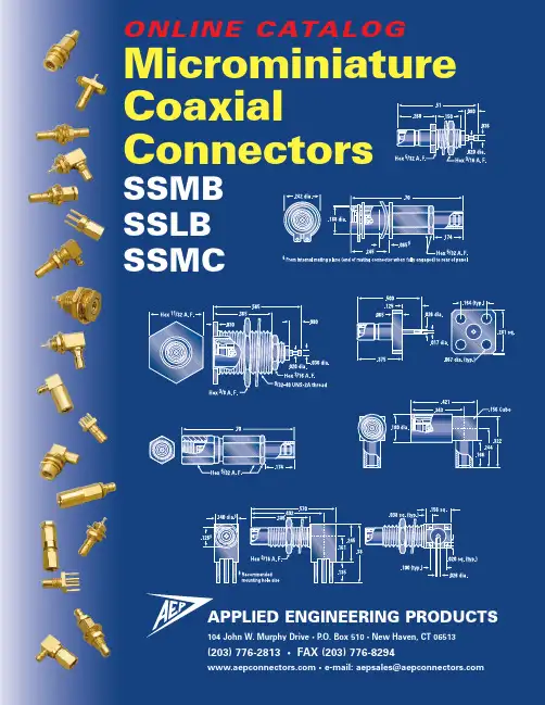
SSMBSSLBSSMCAPPLIED ENGINEERING PRODUCTS104 John W. Murphy Drive • P.O. Box 510 • New Haven, CT 06513Click at the bottom of any page to go to the AEP website.APPLIED ENGINEERING PRODUCTSIntroduction . . . . . . . . . . . . . . . . . . . . . . . . . . . . . . . . . . . . . . . . . . . . . . . . . . . . . . . . . . 2Technical InformationSpecial features and options. . . . . . . . . . . . . . . . . . . . . . . . . . . . . . . . . . . . . . . . . . . . . 3Mated-pair dimensions . . . . . . . . . . . . . . . . . . . . . . . . . . . . . . . . . . . . . . . . . . . . . . . . . 4Interfaces and specifications. . . . . . . . . . . . . . . . . . . . . . . . . . . . . . . . . . . . . . . . . . . . . 5VSWR data. . . . . . . . . . . . . . . . . . . . . . . . . . . . . . . . . . . . . . . . . . . . . . . . . . . . . . . . . . . 6SSMB SeriesCable connectors. . . . . . . . . . . . . . . . . . . . . . . . . . . . . . . . . . . . . . . . . . . . . . . . . . . . . . 7Bulkhead mounted receptacles. . . . . . . . . . . . . . . . . . . . . . . . . . . . . . . . . . . . . . . . . . . 9P .C. board receptacles . . . . . . . . . . . . . . . . . . . . . . . . . . . . . . . . . . . . . . . . . . . . . . . . . 10Panel mounted receptacles. . . . . . . . . . . . . . . . . . . . . . . . . . . . . . . . . . . . . . . . . . . . . 14Adapters . . . . . . . . . . . . . . . . . . . . . . . . . . . . . . . . . . . . . . . . . . . . . . . . . . . . . . . . . . . 14SSLB SeriesCable connectors. . . . . . . . . . . . . . . . . . . . . . . . . . . . . . . . . . . . . . . . . . . . . . . . . . . . . 15Vibration-proof float mount plugs. . . . . . . . . . . . . . . . . . . . . . . . . . . . . . . . . . . . . . . . 16Bulkhead mounted receptacles. . . . . . . . . . . . . . . . . . . . . . . . . . . . . . . . . . . . . . . . . . 17P .C. board receptacles . . . . . . . . . . . . . . . . . . . . . . . . . . . . . . . . . . . . . . . . . . . . . . . . . 18SSMC SeriesCable connectors. . . . . . . . . . . . . . . . . . . . . . . . . . . . . . . . . . . . . . . . . . . . . . . . . . . . . 20Bulkhead mounted receptacles. . . . . . . . . . . . . . . . . . . . . . . . . . . . . . . . . . . . . . . . . . 22P .C. board receptacles . . . . . . . . . . . . . . . . . . . . . . . . . . . . . . . . . . . . . . . . . . . . . . . . . 23Panel mounted receptacles. . . . . . . . . . . . . . . . . . . . . . . . . . . . . . . . . . . . . . . . . . . . . 27Adapters . . . . . . . . . . . . . . . . . . . . . . . . . . . . . . . . . . . . . . . . . . . . . . . . . . . . . . . . . . . 27P .C. Board Mounted Cable Terminations . . . . . . . . . . . . . . . . . . . . . . . . . . . . . . . . . . 28Index by AEP Part Number . . . . . . . . . . . . . . . . . . . . . . . . . . . . . . . . . . . . . . . . . . . . . 29About AEP . . . . . . . . . . . . . . . . . . . . . . . . . . . . . . . . . . . . . . . . . . . . . . . . . . . . . . . . . . 30Other AEP Product Lines . . . . . . . . . . . . . . . . . . . . . . . . . . . . . . . . . . . . . . . . . . . . . . . 31(Click on any line to jump to the page)SMB.237"SSMB P.C. BOARD SMA P.C. BOARD.625".510"Straight PCB receptacle and right angle cable plugComputer-controlled, automated solder-dipping equipment and custom fixturing ensure precise, consistent coverage to AEP standard specification (see above), P a n e lP.C. boardPanel P.C. boardPanelP a n e lC . b o a r dP.C. boardP.C. boardP.C. boardSolder(center conductor)Printed circuit boardSolder(bottom legs and center conductor)Printed circuit boardP .C. Board Receptacles with Standoff LegsPlugPlugClosed-entry contact accepts .014–.015 dia. pinClosed-entry contact accepts .014–.015 dia. pin.000 min..033 min..122 min.Specification requirement Actual(Connectors tested using 200' of cable as load.).53Hex 5/32 A. F..70Hex 5/32 A. F.AEP P/N .46Hex 5/32 A. F..63Hex 5/32 A. F.AEP P/N AEP P/NHex 5/32 A. F.16 A. F.§ Recommended mounting hole size,§ Recommended mounting hole size,Hex 5/32 A. F.16 A. F.16 A. F..386.140 dia.16 A. F..386.140 dia..126.150Hex 3.020 dia..140 dia.§ Recommended mounting hole size,.360Hex 16 A. F.§ Recommended mounting hole size,Hex 3/8 A. F..15016 A. F..036 dia..020 dia..140 dia.§§ Recommended mounting hole size,16 A. F..020 dia..156 sq.16 A. F..020 dia..156 sq..135.419.284.100 (typ.).038 sq. (typ.).156 sq..155.264.156 sq..026 dia..155.419.156 sq..026 dia..025.264.156 sq..026 dia..135.100 (typ.).100 (typ.).020 (typ.).156 sq..141.038 (typ.).080.026 dia.LEG FINISH AEP P/N16 A. F..126§.155.386§ Recommendedmounting hole size,.156 sq..026 dia.16 A. F..135.386.126§§ Recommendedmounting hole size,tolerance +.003, -.000.100 (typ.).038 sq. (typ.).156 sq..38616 A. F..025.126§§ Recommendedmounting hole size,tolerance +.003, -.000.156 sq..026 dia.16 A. F..126§.155.386§ Recommendedmounting hole size,tolerance +.003, -.000.156 sq..026 dia..100 (typ.)16 A. F..386§ .140 dia.16 A. F..386.135.100 (typ.).026 dia..140 dia.16 A. F..386mounting hole size, tolerance +.003, -.000.140 dia..126.038 (typ.).026 dia.16 A. F..386.141.140 dia..020 (typ.).156 sq..135.100 (typ.) .038 sq. (typ.).187dia..155.187dia..187 dia..026 dia..067 dia. (typ.).017 dia..375.125.067 dia. (typ.).026 dia..017 dia..360Hex 5/§ Recommended mounting hole size,16 A. F..360Hex 5/16 A. F.§ Recommended mounting hole size,.53Hex 5/32 A. F..70Hex 5/32 A. F.AEP P/NHex 5/32 A. F.16 A. F.§ Recommended mounting hole size,§ Recommended mounting hole size,Hex 5/32 A. F.16 A. F.§.06516 A. F..020 dia..156 sq..360Hex 16 A. F.§ Recommended mounting hole size,Hex 3/8 A. F.16 A. F..020 dia..156 sq..15016 A. F..036 dia..020 dia..140 dia.§ Recommended mounting hole size,.135.419.284.100 (typ.).038 sq. (typ.).156 sq..155.264.156 sq..026 dia..155.419.156 sq..026 dia..025.264.026 dia..135.100 (typ.).100 (typ.).141.020 (typ.).156 sq..038 (typ.).080.026 dia.LEG FINISH AEP P/N.135.337.100 (typ.).038 sq. (typ.).187 dia..155.317.187 dia..187 dia..026 dia..70Hex 5/32 A. F.AEP P/N .46Hex 5/32 A. F..63Hex 5/32 A. F.AEP P/N AEP P/N Hex 5/32 A. F..19Hex 5/32 A. F..360§ Recommended mounting hole size,16 A. F.Hex 5/32 A. F..360§ Recommended mounting hole size,16 A. F.16 A. F..386.140 dia.16 A. F..386.140 dia..150Hex 3.020 dia..140 dia.§ Recommended mounting hole size,.360Hex 16 A. F.§ Recommended mounting hole size,.135.419.284.100 (typ.).038 sq. (typ.).156 sq..155.264.156 sq..026 dia..155.419.156 sq..026 dia..025.264.156 sq..026 dia..135.100 (typ.).100 (typ.).100 (typ.).038 (typ.).080.026 dia./16 A. F..126§.155.386§ Recommended mounting hole size,tolerance +.003, -.000.156 sq..026 dia.16 A. F..135.386.126§§ Recommendedmounting hole size,tolerance +.003, -.000.100 (typ.).038 sq. (typ.).156 sq..38616 A. F..025.126§§ Recommendedmounting hole size,tolerance +.003, -.000.156 sq..026 dia.16 A. F..126§.155.386§ Recommendedmounting hole size,tolerance +.003, -.000.156 sq..026 dia.16 A. F..386§ .140 dia..100 (typ.).386§ .126.13516 A. F..100 (typ.).026 dia..140 dia..38616 A. F..140 dia..126.038 (typ.).026 dia..386.14116 A. F..140 dia..020 (typ.).156 sq..155 .317.187 dia.Hex 5/(P.C. board thickness).472Hex 5/32 A. F..375.125.017 dia..067 dia. (typ.).375.125.067 dia. (typ.).026 dia..017 dia..360Hex 5/§ Recommended mounting hole size,16 A. F..360Hex 5/§ Recommended mounting hole size,16 A. F..135.314.100 (typ.).038 sq. (typ.).156 sq..155.294.156 sq..026 dia..155.45.156 sq..026 dia..135.100 (typ.).026 dia..100 (typ.).141.020 (typ.).156 sq..038 (typ.).080.026 dia.LEG FINISH AEP P/NAPPLIED ENGINEERING PRODUCTS • aepsales@ 29Index by Part NumberP/N P a g e 5011-1503-000. . . . . . . . .14 5013-1503-000. . . . . . . . .27 5937-1503-000. . . . . . . . .14 5938-1503-000. . . . . . . . .27 7002-1541-0X X*. . . . . . . .20 7002-1571-0X X*. . . . . . . .20 7003-1542-0X X*. . . . . . . .21 7003-1572-0X X*. . . . . . . .21 7004-1512-000. . . . . . . . .22 7009-1511-000. . . . . . . . .23 7009-1511-004. . . . . . . . .23 7009-1511-005. . . . . . . . .23 7009-1511-040. . . . . . . . .23 7009-1511-041. . . . . . . . .23 7009-1511-050. . . . . . . . .23 7009-1511-061. . . . . . . . .23 7010-1511-000. . . . . . . . .23 7010-1511-015. . . . . . . . .23 7010-1511-040. . . . . . . . .23 7010-1511-041. . . . . . . . .23 7010-1511-050. . . . . . . . .23 7010-1511-060. . . . . . . . .23 7010-1511-061. . . . . . . . .23 7012-1511-000. . . . . . . . .22 7017-1512-000. . . . . . . . .22 7022-1502-000. . . . . . . . .14 7022-1502-000. . . . . . . . .27 7025-1512-000. . . . . . . . .26 7025-1512-012. . . . . . . . .26 7025-1512-015. . . . . . . . .26 7025-1512-040. . . . . . . . .26 7025-1512-050. . . . . . . . .26 7025-1512-060. . . . . . . . .26 7025-1512-061. . . . . . . . .26 7029-1511-000. . . . . . . . .24 7029-1511-012. . . . . . . . .24 7029-1511-015. . . . . . . . .24 7029-1511-015. . . . . . . . .24 7029-1511-040. . . . . . . . .24 7029-1511-060. . . . . . . . .24 7029-1511-061. . . . . . . . .24 7040-1511-000. . . . . . . . .22 7042-1511-000. . . . . . . . .26 7042-1511-012. . . . . . . . .26 7042-1511-015. . . . . . . . .26 7042-1511-040. . . . . . . . .26 7042-1511-050. . . . . . . . .26 7042-1511-060. . . . . . . . .26 7042-1511-061. . . . . . . . .26 7101-1541-0X X*. . . . . . . .20 7101-1571-0X X*. . . . . . . .20 7105-1521-0X X*. . . . . . . .20 7105-1561-0X X*. . . . . . . .20 7106-1521-0X X*. . . . . . . .21 7106-1561-0X X*. . . . . . . .21 7110-1511-000. . . . . . . . .25 7110-1511-012. . . . . . . . .25 7110-1511-015. . . . . . . . .25 7110-1511-040. . . . . . . . .25 7110-1511-050. . . . . . . . .25 7110-1511-060. . . . . . . . .25 7110-1511-061. . . . . . . . .25 7119-1512-000. . . . . . . . .22P/N P a g e7122-1502-000. . . . . . . . .277141-1562-0X X*. . . . . . . .217141-1572-0X X*. . . . . . . .217145-1511-0X X*. . . . . . . .287145-1511-1X X*. . . . . . . .287145-1511-2X X*. . . . . . . .287145-1511-3X X*. . . . . . . .287145-1511-4X X*. . . . . . . .287145-1511-5X X*. . . . . . . .287145-1511-6X X*. . . . . . . .287146-1511-0X X*. . . . . . . .287146-1511-1X X*. . . . . . . .287146-1511-2X X*. . . . . . . .287146-1511-3X X*. . . . . . . .287146-1511-4X X*. . . . . . . .287146-1511-5X X*. . . . . . . .287198-1513-000. . . . . . . . .277199-1513-000. . . . . . . . .277201-1541-0X X*. . . . . . . .77201-1571-0X X*. . . . . . . .77202-1542-0X X*. . . . . . . .77202-1572-0X X*. . . . . . . .77203-1541-0X X*. . . . . . . .87203-1571-0X X*. . . . . . . .87204-1511-000. . . . . . . . . .97209-1511-000. . . . . . . . .107209-1511-011. . . . . . . . .107209-1511-015. . . . . . . . .107209-1511-023. . . . . . . . .107209-1511-040. . . . . . . . .107209-1511-061. . . . . . . . .107210-1511-000. . . . . . . . .107210-1511-015. . . . . . . . .107210-1511-040. . . . . . . . .107210-1511-050. . . . . . . . .107210-1511-060. . . . . . . . .107210-1511-061. . . . . . . . .107212-1511-000. . . . . . . . . .97217-1512-000. . . . . . . . . .97219-1511-000. . . . . . . . . .97222-1501-000. . . . . . . . .147225-1512-000. . . . . . . . .137225-1512-012. . . . . . . . .137225-1512-015. . . . . . . . .137225-1512-040. . . . . . . . .137225-1512-050. . . . . . . . .137225-1512-060. . . . . . . . .137225-1512-061. . . . . . . . .137229-1511-000. . . . . . . . .117229-1511-012. . . . . . . . .117229-1511-015. . . . . . . . .117229-1511-040. . . . . . . . .117229-1511-050. . . . . . . . .117229-1511-060. . . . . . . . .117229-1511-061. . . . . . . . .117240-1511-000. . . . . . . . . .97242-1511-000. . . . . . . . .137242-1511-012. . . . . . . . .137242-1511-015. . . . . . . . .137242-1511-040. . . . . . . . .137242-1511-050. . . . . . . . .137242-1511-060. . . . . . . . .137242-1511-061. . . . . . . . .13P/N P a g e7302-1542-0X X*. . . . . . . .157302-1572-0X X*. . . . . . . .157303-1541-0X X*. . . . . . . .167303-1571-0X X*. . . . . . . .167304-1511-000. . . . . . . . .177305-1521-0X X*. . . . . . . .157305-1561-0X X*. . . . . . . .157309-1511-000. . . . . . . . .187309-1511-012. . . . . . . . .187309-1511-015. . . . . . . . .187309-1511-040. . . . . . . . .187309-1511-050. . . . . . . . .187309-1511-060. . . . . . . . .187309-1511-061. . . . . . . . .187310-1511-000. . . . . . . . .187310-1511-012. . . . . . . . .187310-1511-015. . . . . . . . .187310-1511-040. . . . . . . . .187310-1511-050. . . . . . . . .187310-1511-060. . . . . . . . .187310-1511-061. . . . . . . . .187312-1511-000. . . . . . . . .177317-1511-000. . . . . . . . .177325-1512-000. . . . . . . . .197325-1512-012. . . . . . . . .197325-1512-015. . . . . . . . .197325-1512-040. . . . . . . . .197325-1512-050. . . . . . . . .197325-1512-060. . . . . . . . .197325-1512-061. . . . . . . . .197332-1571-0X X*. . . . . . . .167332-1571-2X X*. . . . . . . .167335-1571-0X X*. . . . . . . .167335-1571-2X X*. . . . . . . .167340-1511-000. . . . . . . . .177341-1561-0X X*. . . . . . . .157341-1571-0X X*. . . . . . . .157342-1511-000. . . . . . . . .197342-1511-012. . . . . . . . .197342-1511-015. . . . . . . . .197342-1511-040. . . . . . . . .197342-1511-050. . . . . . . . .197342-1511-060. . . . . . . . .197342-1511-061. . . . . . . . .197396-1512-000. . . . . . . . .177405-1521-0X X*. . . . . . . .77405-1561-0X X*. . . . . . . .77406-1521-0X X*. . . . . . . .87406-1561-0X X*. . . . . . . .87410-1511-000. . . . . . . . .127410-1511-012. . . . . . . . .127410-1511-015. . . . . . . . .127410-1511-040. . . . . . . . .127410-1511-050. . . . . . . . .127410-1511-060. . . . . . . . .127410-1511-061. . . . . . . . .127441-1561-0X X*. . . . . . . .87441-1571-0X X*. . . . . . . .87496-1512-000. . . . . . . . . .97498-1513-000. . . . . . . . .147499-1513-000. . . . . . . . .14* Indicates cable connectors with varioustypes on specified page.(Click on any line to jump to the page)(203) 776-2813 • FAX (203) 776-8294APPLIED ENGINEERING PRODUCTS • aepsales@ 30About Applied Engineering ProductsSince our foundation in 1973, we have always believed that having our customers take a look “inside AEP” is important in fostering strong vendor/customer relationships. We are proud of our physical plant and equipment, but even more so of our dedicated staff. When customers see first-hand how AEP’s people keep a constant focus on maintaining and improvingcustomer service and satisfaction, the rea-son for our consistently strong on-timedelivery and quality records becomes clear.We invite you to see for yourself. Call us toarrange a plant tour—or, if you can’t makea visit, ask for your copy of INSIDE AEP,our facilities and capabilities brochure.(203) 776-2813 • FAX (203) 776-829431The SSMB, SSLB, and SSMC connectors in this brochure are only part of our complete line of subminiature coaxial connectors and cable assemblies, including:• MCX• MMCX• SMA• SMB• SMC• SSMA• SSMB• SSMC• SLB (Slide-on version of SMB)• SSLB (Slide-on version of SSMB)• 75ΩMiniature SMB• 75ΩSnap-on mating• 75ΩScrew-on mating• Adapters within and between series• Flexible cable assemblies• Semi-rigid cable assemblies• And over 100 styles of MIL-PRF-39012 QPL connectorsin series SMA, SMB, and SMCAPPLIED ENGINEERING PRODUCTS104 John W. Murphy Drive • P .O. Box 510 • New Haven, CT 06513(203) 776-2813• FAX (203) 776-8294 • e-mail: aepsales@。


Analysis…Napoleon notoriously said that if France catches a cold, the whole world does too. Now it is said that if America sneezes, the world catches its cold. What if America catches a cold? What will happen to the world? A query like this seems vital in the aftermath of the newest events, which has affected the United States and caused extensive harm and loss both in human and economic terms.Only a remarkable diplomatic initiative at this point could bring about the common understanding needed for "a collective solution," which would be the only way out of the global economic crisis, perhaps the vision of the abyss will stimulate a spirit of cooperation among government leaders.After three decades of globalization, the worldwide system of production of goods and services is integrated, and it would be seriously disrupted if an epidemic of protectionism blocks the flow of trade and investment. The general reaction will be greater control over capital flows, as a first step. If that does not work, there will be a tidal wave of trade protectionism, which will slow down economic activity in the emerging countries that are shoring up the global economy.Today, the situation is different: the goal is to overcome recession and devalue the dollar to increase exports, to the detriment of trading partners. But emerging countries nowadays have means to defend themselves. The government needs to adopt other measures "to select" capital inflows, including the requirement that investment must remain in the country for a specified period.Peak oil also means that travel of any sort will also get more expensive, and long trips abroad might be out of the means of most of us. As a result, more of us will vacation closer to home, and perhaps will discover the charms of our own community.If people are staying home more, they might also be more inclined to get involved in their community. Maybe we'll see a return to people talking to others at public events and finding out about their neighbors.It’s said that, in fact, every country always tries to transfer internal problems outside itself, but actions by great powers have effects of a different magnitude, and in today's world "everyone reacts, so a very dangerous period is opening up, with unlimited potential for conflicts."Some things from the past we might not like to repeat, but there were a lot of good things too, and a smaller world might be one that works well for us in the future.。
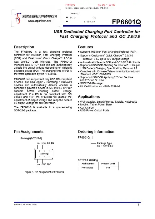
FP6601QUSB Dedicated Charging Port Controller for Fast Charging Protocol and QC 2.0/3.0Pin AssignmentsPackage(SOT-23-6)(Marking)213645GND FBOD+D-QC_ENVDDFigure 1. Pin Assignment of FP6601QOrdering InformationFP6601Q□Package Type S6: SOT-23-6DescriptionThe FP6601Q is a fast charging protocol controller for HiSilicon Fast Charging Protocol(FCP) and Qualcomm ® Quick Charge TM2.0/3.0 (QC 2.0/3.0) USB interface. The FP6601Q monitors USB D+/D− data line and automatically adjusts the output voltage depending on different powered device (PD). The charging time of PD is therefore optimized by the FP6601Q.FP6601Q can support not only USB BC compliant devices, but also Apple / Samsung / HUAWEI devices and automatically detects whether a connected powered device is QC 2.0/3.0 or FCP capable before enabling output voltage adjustment. If a PD is not compliant with QC 2.0/3.0 and FCP , the FP6601Q will disable the adjustment of output voltage and keep the default 5V output voltage for safe operation.The FP6601Q is available in a space-saving SOT-23-6 package.Features● Supports HiSilicon Fast Charging Protocol (FCP)● Supports Qualcomm ® Quick Charge TM2.0/3.0Class A : 3.6V up to 12V Output Voltage● Automatically Selects FCP and QC2.0/3.0 Protocols ● Supports USB DCP Shorting D+ Line to D − Line per USB Battery Charging Specification, Revision 1.2 ● Complies with Chinese Telecommunication Industry Standard YD/T 1591-2009● Supports USB DCP Applying 2.7V on D+ Line and 2.7V on D − Line ● SOT-23-6 Package● UL Certification No. 4787452994-2Applications● Wall-Adapter, Smart Phones, Tablets, Notebooks ● Mobile / Tablet Power Bank ● Car Charger● USB Power Output PortsFP6601Q 资料更新:●D+,D-脚的耐压提高至14V●反馈电压范围0.4V-1.5VFP6601Q 工作设计原理解说(AC-DC / DC-DC ):/product/275.htmlTypical Application CircuitNode VOUT D −D+GNDFigure 2. Typical Application SchematicNote 1: The recommended voltage of feedback node ranges between 0.4V and 1.5VOutput Voltage Lookup Table(QC 2.0/3.0)QC20/QC30典型应用方案NS6116车载充电器( )Functional Pin DescriptionBlock DiagramD −D+FBOQC_ENFigure 3. Block Diagram of FP6601QAbsolute Maximum Ratings (Note 2)● Input Supply Voltage VDD ------------------------------------------------------------------------------ -0.3V to +7V● D+,D−Pins Voltage --------------------------------------------------------------------------------------- -0.3V to +14V● All Other Pins Voltage ----------------------------------------------------------------------------------- -0.3V to +7V● Maximum Junction Temperature (T J)----------------------------------------------------------------- +150℃● Storage Temperature (T S)------------------------------------------------------------------------------- -65℃ to +150℃● Lead Temperature (Soldering, 10sec.) -------------------------------------------------------------- +260°C● Package Thermal Resistance, (θJA) (Note 3)SOT-23-6---------------------------------------------------------------------------------------- 250°C/W● Package Thermal Resistance, (θJC)SOT-23-6---------------------------------------------------------------------------------------- 110°C/WNote 2: Stresses beyond this listed under “Absolute Maximum Ratings" may cause permanent damage to the device. Note 3: θJA is measured at 25°C ambient with the component mounted on a high effective thermal conductivity test board of JEDEC-51-7.Recommended Operating Conditions● Input Supply Voltage (VDD)---------------------------------------------------------------------------- +3.2V to +6.8V● Operation Temperature Range (T OPR) -------------------------------------------------------------- -40°C to +85°CElectrical CharacteristicsElectrical Characteristics (Continued)Note 3: Not production tested.Typical Performance CurvesFigure 4. UP Current vs. Temperature Figure 5. Supply Current vs. TemperatureApplication InformationFunction DescriptionThe FP6601Q integrates both USB high voltage dedicated charging port interface IC for Qualcomm ®Quick Charge TM2.0/3.0 class A andHiSiliconFCP specification.The FP6601Q can fast charge most of the handheld devices. It could be treated as the original charging adapter.The FP6601Q supports BC1.2, Samsung and HUAWEI devices. It also supports output voltage range of QC 3.0 Class A (3.6V to 12V) or QC 2.0 Class A (5V, 9V, 12V).Quick Charge 2.0/3.0 InterfaceWhen the FP6601Q is powered on, D+ and D − pin are applied to 2.7V for Apple device. If handheld device has the function of QC 2.0/3.0, D+ pin will be forced between 0.325V and 2V. In the meanwhile, D+ pin will short to D − pin through the switch SW1 for entering BC 1.2. If D+ is continuously applied to the voltage between 0.325V and 2V for 1.25 seconds, the FP6601Q will enter QC 2.0/3.0 or FCP operation mode.When the voltage of D+ pin and D − pin simultaneously satisfy these two inequalities V DAT(REF)< D+ <V SEL_REF and D − > V SEL_REF , the FP6601Q would enter continuous mode.In the continuous mode, each voltage pulse on D+ pin generated by powered device is between 1V and 3V. In the meanwhile, the high level of pulse should be keep at least 200us. If the specified conditions are satisfied, the FBO pin will sink 2uA per pulse. The maximum sink current is 70uA for output voltage 12V.In the continuous mode, each voltage pulse on D − pin generated by powered device is between 3V and 1V. At the same time, the low level of pulse should be keep at least 200us. If the specified conditions are satisfied, the FBO pin will source 2uA per pulse. The maximum source current is 14uA for output voltage 3.6V.If the powered device does n’t support QC 2.0, the FP6601Q will remain default output voltage 5V for safe operation. On the other hand, when USB cable is removed, the voltage of D+ pin is therefore lower than V DAT(REF) and the output default voltage 5V is also applied. Shunt RegulatorThe VDD of FP6601Q is supplied by the wide output voltage through the external resistor RVDD. The internal Zener-Diode is utilized to clamp the VDD at 6.4V. The recommended value of RVDD and CVDD are 2.2k Ω and 470nF, respectively. QC_EN FunctionQC 2.0/3.0 and FCP function are disabled by connecting the QC_EN pin to ground. On the contrary, QC 2.0/3.0 and FCP function could be enabled by connecting QC_EN pin to VDD or high-Z. Additionally, when FP6601Q is already accessed QC 2.0/3.0 or FCP mode, the selected mode can ’t be changed by setting QC_EN pin. Data Line ProtectionWhen D+/D − pin is touched by the output voltage in abnormal situation, the D+/D − pin of both sink device and source device may be damaged. In order to protect the D+/D − pin of the devices from damage in abnormal situation, the FP6601Q will return the output voltage to default output voltage 5V when the voltage of D+/D − pin is touched larger than 7.5V.Outline InformationSOT-23-6 Package (Unit: mm)Carrier DimensionsLife Support PolicyFitipower’s products are not authorized for use as critical components in life support devices or other medical systems.。
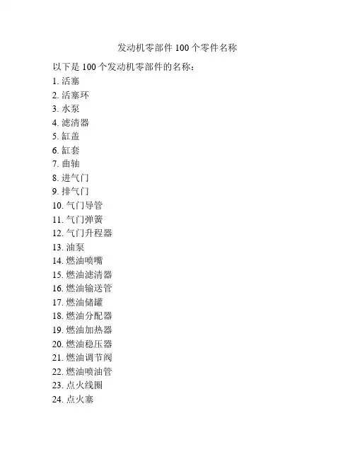
发动机零部件100个零件名称以下是100个发动机零部件的名称:1. 活塞2. 活塞环3. 水泵4. 滤清器5. 缸盖6. 缸套7. 曲轴8. 进气门9. 排气门10. 气门导管11. 气门弹簧12. 气门升程器13. 油泵14. 燃油喷嘴15. 燃油滤清器16. 燃油输送管17. 燃油储罐18. 燃油分配器19. 燃油加热器20. 燃油稳压器21. 燃油调节阀22. 燃油喷油管23. 点火线圈24. 点火塞25. 点火线管26. 点火线接头27. 点火控制模块28. 点火触发装置29. 点火式起动机30. 点火线圈信号发生器31. 曲轴座泵32. 曲轴箱前盖33. 冷却液箱34. 温度传感器35. 管路组件36. 管路连接螺纹垫圈37. 先导阀38. 流量计39. 油门执行器40. 空气进气口41. 空气过滤器42. 进气歧管43. 进气歧管温度传感器44. 进气压力传感器45. 进气温度传感器46. 进气体积流量传感器47. 排气管48. 排气催化器49. 排气氧传感器50. 排气温度传感器51. 排气压力传感器52. EGR阀53. EGR冷却器54. 燃油蒸发控制系统55. 转向泵56. 润滑油泵57. 燃油泵嘴58. 燃油运行系统59. 机油冷却器60. 机油滤清器61. 润滑系统管路62. 卧式滤清器63. 进气音箱64. 空气管道65. 增压器66. 变速器67. 水箱散热器68. 反向螺旋风扇69. 机油滤芯70. 涡轮增压器71. 进气道72. 凸轮轴73. 燃油喷雾嘴74. 机油泵喉75. 涡轮增压器轴承76. 高温排气涡轮77. 油泵零件78. 冷却水泵零件79. 主曲轴零件80. 汽门机构零件81. 涡轮增压器零件82. 进气歧管零件83. 进气管零件84. 排气歧管零件85. 排气管零件86. 发动机缸盖零件87. 发动机机体零件88. 发动机块零件89. 飞轮零件90. 启动机零件91. 发电机零件92. 变速器零件93. 电动机控制电磁阀94. 燃油喷射组件95. 触媒96. 凸轮轴齿轮组件97. 双板长曲轴弹簧98. 油滤器负荷控制器99. 涡轮增压器补偿风扇100. 多点喷射直喷油泵。

“Providingtechnologicalleadership inepoxy additives,worldwide.”EpoxyAdditives and ResinsNorth AmericaONE-PA C K,RAPID HEAT C URELOWEST EXUDATION, IMPROVED C OLOR, LOW VIS C OSITYAN C AMINE 2089MAN C AMINE 2410LOW FREE-AMINE ADDU C T, G OOD C HEMI C AL RESISTAN C E, FDA-C OMPLIANTBEST LOW-TEMPERATURE C URE, LOW EXUDATION,VERY G OOD C HEMI C AL RESISTAN C EAN C AMINE 1856LON G POT LIFE,BEST C OLOR STABILITY,LOW EXUDATIONAN C AMINE 1784AN C AMINE 2014AS/2014F GLOWER VIS C OSITY,LOWER LOADIN G VARIANTAN C AMINE 1638AN C AMINE 2432BEST C HEMI C AL RESISTAN C E, G OOD LOW-TEMPERATURE C URE, G OOD POT LIFE, LOW VIS C OSITYLOWEST BLUSH KETIMINEAN C AMINE 2459LOW VIS C OSITY KETIMINE,LON G EST POT LIFEAN C AMINE 2458LOW VIS C OSITY KETIMINE,HI G HEST FILM BUILD C OATIN GAN C AMINE 2457G OOD RESISTAN C E TO C HEMI C ALS AND HOT WATERAN C AMINE ® 1608AN C AMINE 2481RAPID C URE,EX C ELLENT FILM APPEAREN C EAN C AMINE 2641VERY RAPID C URE AND PROPERTY DEVELOPMENT,FAST LOW-TEMPERATURE C URE,PHENOL-FREEIMPROVED LOW-TEMPERATURE C UREAN C AMINE 1637-LVAN C AMINE 1768LOW VIS C OSITY,G OOD C OLOR,FAST C UREAN C AMINE 2526LOW VIS C OSITY,LOW C OLOR,FAST C URE,LON G ER POT LIFEAN C AMINE 2441/2442EX C ELLENT REA C TIVITY,EX C ELLENT G REEN STREN G TH,G OOD FORMULATION SHELF STABILITY,HI G H G LASS TRANSITION TEMPERATUREAN C AMINE 2422EX C ELLENT C HEMI C AL RESISTAN C E, G OOD POT LIFE, SUITABLE FOR AMBIENT C URE OR POST C UREONE-TO-ONE MIX RATIOS,HI G H TEAR RESISTAN C E, TENSILE STREN G TH AND ELON G ATION,G OOD C HEMI C AL RESISTAN C EAN C AMINE 2390AN C AMINE 2143BE S T C OLOR S TABILITY, G OOD C HEMI C AL AND BLU S H RE S I S TAN C E AN C AMINE 1618AN C AMINE® 2280EX C ELLENT C HEMI C AL RE S I S TAN C E, VERY G OOD FILM APPEARAN C E,BE S T BLU S H ANDWATER S POT RE S I S TAN C E AN C AMINE 2505RAPID LOW TEMPERATURE C URE,VERY G OOD BLU S H ANDWATER S POT RE S I S TAN C E,VERY G OOD C HEMI C ALRE S I S TAN C EVERY G OOD C HEMI C AL RE S I S TAN C E,BE S T HOT OIL RE S I S TAN C EAN C AMINE 2334AN C AMINE 2587IMPROVED S OLVENT RE S I S TAN C E,HI G H TEMPERATURE RE S I S TAN C EAN C AMINE 2368FA S T C URE S PEED,HI G H S TREN G TH AND MODULU S AN C AMINE 1693IMPROVED MEK AND AL C OHOLRE S I S TAN C E, LOW VI SC O S ITYAN C AMINE 2423FA S TE S T C URE AT AMBIENT ANDLOW TEMPERATURE S,BE S T OR G ANI C A C ID RE S I S TAN C EVERY LOW VI SC O S ITY,LOW MIX VI SC O S ITY,RAPID PROPERTY DEVELOPMENT ATLOW TEMPERATUREAN C AMINE 2489LOWE S T VI SC O S ITY, LOW C OLORAN C AMINE 2286G OOD C OLOR S TABILITYAND FLEXIBILITY, FA S TER C UREAN C AMINE 2074EX C ELLENT MOI S TURE TOLERAN C E,G OOD LOW- TEMPERATURE C UREAN C AMINE M C ALON G WORKIN G LIFE,LOWE S T U S A G E RATEAN C AMINE 1884AN C AMINE 2605EX C ELLENT LOW TEMP C URE,G OOD BLU S H RE S I S TAN C E ANDWATER S POT RE S I S TAN C EEX C ELLENT C OLOR S TABILITY,G OOD C HEMI C AL RE S I S TAN C EG OOD C OLOR,C OLOR S TABILITY AND G LO SSAN C AMINE 2579LON G ER POT LIFE VARIANT OF AN C AMIDE 500AN C AMIDE 506AN C AMIDE 502S TANDARD AMIDOAMINE, LOW VI SC O S ITY, MEDIUM POT LIFEAN C AMIDE ® 500BE S T C HEMI C AL RE S I S TAN C E, EX C ELLENT ADHE S ION TO DAMP C ON C RETEAN C AMIDE 2396A CC ELERATED C URE,G OOD C HEMI C AL RE S I S TAN C EAN C AMIDE 501IMPROVED FILM FORMATION,VERY G OOD C HEMI C AL RE S I S TAN C EAN C AMIDE 2386FA S TER C URE VARIANT OF AN C AMIDE 500AN C AMIDE 503FA S T C URE,IMPROVED WATER RE S I S TAN C EAN C AMIDE 507VERY LOW VI SC O S ITY, LON G POT LIFE,EX C ELLENT ADHE S ION TO POORLY PREPARED S UB S TRATE SAN C AMIDE 2443LON G POT LIFE,EX C ELLENT FLEXIBILITYAN C AMIDE 2447LON G POT LIFE,G OOD BLU S H RE S I S TAN C E, FDA-C OMPLIANTAN C AMIDE 2426AN C AMIDE® 220STANDARD POLYAMIDE USED WITH SOLID EPOXY RESININ SOLVENTBORNE C OATIN G S STANDARD MEDIUM-VIS C OSITY POLYAMIDE USED WITH LIQUID EPOXY RESINAN C AMIDE 260AAN C AMIDE 350A STANDARD HI G H IMIDAZOLINE, LOWER-VIS C OSITY POLYAMIDE HI G H C ORROSION AND C HEMI C ALRESISTAN C E, BROAD APPLI C ATIONAND TEMPERATURE RAN G E,VERY C OST EFFE C TIVE,HI G H BLUSH RESISTAN C E,G OOD C ATHODI C DISBONDMENTRESISTAN C E,G OOD FLEXIBILITY AND ADHESIONAN C AMIDE 2634ENHAN C ED LOW-TEMPERATURE C URE,RAPID REA C TIVITY,2K ADHESIVE APPLI C ATIONSAN C AMIDE 2424LOW-VIS C OSITY POLYAMIDE ADDU C T,NO INDU C TION,VO C-C OMPLIANT C OATIN G SAN C AMIDE 2050G OOD FILM APPEARAN C E,VERY G OOD LOW TEMPERATUREC URE, BEST C HEMI C ALRESISTAN C E, LOW VIS C OSITYAN C AMIDE 2353LOW-VIS C OSITY ADDU C T,G OOD LOW-TEMPERATURE C UREAN C AMIDE 2445LOW-VIS C OSITY, PLASTI C IZER-FREE,G OOD ADHESION TO METALAND PLASTI C,2K ADHESIVE APPLI C ATIONSAN C AMIDE 2482LOW-VIS C OSITY VARIANTAN C AMIDE 375AVER Y HI G H FLEXIBILITYAND PEEL STREN G TH,EX C ELLENT THERMAL SHO C KRESISTAN C EAN C AMIDE 910LOW VIS C OSITY VARIANT,RAPID C URE, PLASTI C IZER-FREEAN C AMIDE 805EX C ELLENT HI G H G LOSSFILM FORMATION,FAST-DRY WITH NO INDU C TION TIMEAN C AMIDE 2444NMP-FREEHYBRIDUR ® 878NMP-FREEHYBRIDUR 870WOOD OR HARD PLA S TI CHYBRIDUR 580FLEXIBLE S UB S TRATE SHYBRIDUR 560METAL OR C ON C RETEHYBRIDUR 570S OLVENT, SC UFF RE S I S TAN C EHYBRIDUR 540C ONTAIN NMPHARD SOFTTalk direct to a technical representative at 800-345-3148 or 610-481-6799.* Approved regi s tration required. C ontact Air Product s for more information on how to become an APDirect on-line buyer.ABOUT USBUSINESS OVERVIEW TE C HNI C AL NEWSSTANDFDA LETTERS MSDS LIBRARY SAMPLE ORDERIN G PRODU C T ORDERIN G*NEW DEVELOPMENTS RE C ENT NEWS RELEASES TE C HNI C AL PAPERS G LOSSARY OF TERMSINDUSTRIAL C OATIN G S ADHESIVESC IVIL EN G INEERIN G C OMPOSITESMARKET PRODU C T OFFERIN GPRODU C T INFORMATION PA G EPRODU C T MSDS (PDF )PRODU C T SALES SPE C IFI C ATION (PDF )STOI C HIOMETRY C AL C ULATION G UIDE SAMPLE ORDERIN G PRODU C T ORDERIN G*PRODU C T SPE C IFIERSFORMULATIN G /APPLI C ATION INFORMATIONAPPLI C ATION LITERATURE (PDF FILE S )STARTIN G POINT FORMULATIONS (PDF FILE S )FORMULATIN G TIPSASK THE EXPERTS — TE C HNI C AL Q &APRODU C T DATA SHEET (PDF )• A compari s on of product performance for key performance criteria • Product name s link to product information page s• Regi s tration with immediate acce ss i s required to get the following information:Click on product name to access:Links to:Each market segment includes:NORTH AMERI C AN HOME PA G EMARKET SE G MENTSE-LEARNIN G C ENTERPRODU C T FINDER A library of narrated PowerPointpre s entation s on the late s t Epoxy Additive and Re s in informationSUBS C RIBE TO EPOXY E-NEWSLETTEREPOXY E-LEARNIN G C ENTER PRODU C T DATA SHEET (PDF )PRODU C T MSDS (PDF )PRODU C T SALES SPE C IFI C ATION (PDF )STOI C HIOMETRY C AL C ULATION G UIDE SAMPLE ORDERIN G PRODU C T ORDERIN G*PRODU C T LISTIN G• C hoo s e de s ired product type from tab s acro ss top of page• Regi s tration with immediate acce ss i s required to get the following information • C lick on product name to acce ss :PRODU C T INFORMATION PA G EDOT NONRE G ULATED PRODU C T LISTIN GProvides the following information: • G eneral De s cription • Key Advantage s • Key Application s • Typical Propertie s Links to:C OMPLETE PRODU C T OFFERIN GFDA LETTER * IF APPLI C ABLEISO C ERTIFI C ATESWORLDWIDE LO C ATIONS/NORTH AMERI C AN DISTRIBUTORSTE C HNOLO G Y PRESENTATIONS ENVIRONMENTAL, HEALTH & SAFETYPRESENTATIONS4948Air Products’ Epoxy Additives Air Products offers a full lineof high-quality,performance-oriented epoxy curing agentsand modifiers for a wide varietyof applications,including industrial coatings,civil engineering and construction, adhesives,and composites.We also offer a line of high-performance specialty resinsfor waterborne coatings applications.These products are produced at state-of-the-art manufacturing facilities located in Los Angeles, California; Wichita,Kansas; Manchester,England; Isehara, Japan and Singapore. In addition,we maintain numerous stocking points throughout the world.Our experienced technical specialists have an in-depth understanding of your market requirements and are able to provide the right level oftechnical service and supportthat you need.。
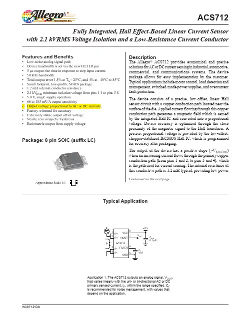
Approximate Scale 1:1Application 1. The ACS712 outputs an analog signal, V OUT . that varies linearly with the uni- or bi-directional AC or DC primary sensed current, I P , within the range specified. C F is recommended for noise management, with values that depend on the application.ACS712DescriptionThe Allegro ® ACS712 provides economical and precise solutions for A C or DC current sensing in industrial, automotive, commercial, and communications systems. The device package allows for easy implementation by the customer. Typical applications include motor control, load detection and management, switched-mode power supplies, and overcurrent fault protection.The device consists of a precise, low-offset, linear Hall sensor circuit with a copper conduction path located near the surface of the die. Applied current flowing through this copper conduction path generates a magnetic field which is sensed by the integrated Hall IC and converted into a proportional voltage. Device accuracy is optimized through the close proximity of the magnetic signal to the Hall transducer. A precise, proportional voltage is provided by the low-offset, chopper-stabilized BiCMOS Hall IC, which is programmed for accuracy after packaging.The output of the device has a positive slope (>V IOUT(Q)) when an increasing current flows through the primary copper conduction path (from pins 1 and 2, to pins 3 and 4), which is the path used for current sensing. The internal resistance of this conductive path is 1.2 mΩ typical, providing low powerFeatures and Benefits▪ Low-noise analog signal path▪ Device bandwidth is set via the new FILTER pin ▪ 5 µs output rise time in response to step input current ▪ 50 kHz bandwidth▪ Total output error 1.5% at T A = 25°C, and 4% at –40°C to 85°C ▪ Small footprint, low-profile SOIC8 package ▪ 1.2 mΩ internal conductor resistance▪ 2.1 kV RMS minimum isolation voltage from pins 1-4 to pins 5-8▪ 5.0 V , single supply operation▪ 66 to 185 mV/A output sensitivity▪ Output voltage proportional to AC or DC currents ▪ Factory-trimmed for accuracy▪ Extremely stable output offset voltage ▪ Nearly zero magnetic hysteresis▪Ratiometric output from supply voltageFully Integrated, Hall Effect-Based Linear Current Sensorwith 2.1 kVRMS V oltage Isolation and a Low-Resistance Current ConductorContinued on the next page…Package: 8 pin SOIC (suffix LC)Typical ApplicationC BYP 0.1 µFSelection GuidePart Number Packing*T OP (°C)Optimized Range, I P(A)Sensitivity, Sens (Typ) (mV/A)ACS712ELCTR-05B-T Tape and reel, 3000 pieces/reel –40 to 85±5185ACS712ELCTR-20A-T Tape and reel, 3000 pieces/reel –40 to 85±20100ACS712ELCTR-30A-TTape and reel, 3000 pieces/reel–40 to 85±3066*Contact Allegro for additional packing options.loss. The thickness of the copper conductor allows survival of the device at up to 5× overcurrent conditions. The terminals of the conductive path are electrically isolated from the sensor leads (pins 5 through 8). This allows the ACS712 current sensor to be used in applications requiring electrical isolation without the use of opto-isolators or other costly isolation techniques.The A CS712 is provided in a small, surface mount SOIC8 package. The leadframe is plated with 100% matte tin, which is compatible with standard lead (Pb) free printed circuit board assembly processes. Internally, the device is Pb-free, except for flip-chip high-temperature Pb-based solder balls, currently exempt from RoHS. The device is fully calibrated prior to shipment from the factory.Description (continued)Absolute Maximum RatingsCharacteristicSymbol NotesRating Units Supply Voltage V CC 8V Reverse Supply Voltage V RCC –0.1V Output VoltageV IOUT 8V Reverse Output Voltage V RIOUT –0.1V Output Current Source I IOUT(Source) 3mA Output Current SinkI IOUT(Sink)10mA Overcurrent Transient Tolerance I P 100 total pulses, 250 ms duration each, applied at a rate of 1 pulse every 100 seconds.60A Maximum Transient Sensed Current I R (max)Junction Temperature, T J < T J (max)60A Nominal Operating Ambient Temperature T A Range E–40 to 85ºC Maximum Junction T J (max)165ºC Storage TemperatureT stg–65 to 170ºCTÜV AmericaCertificate Number: U8V 06 05 54214 010Parameter SpecificationFire and Electric ShockCAN/CSA-C22.2 No. 60950-1-03UL 60950-1:2003EN 60950-1:2001IP+IP+IP–IP–VCC VIOUT FILTER GNDTerminal List TableNumber Name Description1 and 2IP+Terminals for current being sensed; fused internally 3 and 4IP–Terminals for current being sensed; fused internally 5GND Signal ground terminal6FILTER Terminal for external capacitor that sets bandwidth 7VIOUT Analog output signal 8VCCDevice power supply terminalFunctional Block DiagramPin-out DiagramCOMMON OPERATING CHARACTERISTICS1 over full range of T OP , C F = 1 nF, and V CC = 5 V, unless otherwise specified Characteristic Symbol Test Conditions Min.Typ.Max.Units ELECTRICAL CHARACTERISTICSSupply Voltage V CC 4.5 5.0 5.5V Supply Current I CC V CC = 5.0 V, output open6811mA Output Zener Clamp Voltage V Z I CC = 11 mA, T A = 25°C68.3–V Output Resistance R IOUT I IOUT = 1.2 mA, T A=25°C–12ΩOutput Capacitance Load C LOAD VIOUT to GND––10nF Output Resistive Load R LOAD VIOUT to GND 4.7––kΩPrimary Conductor Resistance R PRIMARY T A = 25°C– 1.2–mΩRMS Isolation Voltage V ISORMS Pins 1-4 and 5-8; 60 Hz, 1 minute, T A=25°C2100––V DC Isolation Voltage V ISODC Pins 1-4 and 5-8; 1 minute, T A=25°C–5000–V Propagation Time t PROP I P = I P(max), T A = 25°C, C OUT = open–3–μs Response Time t RESPONSE I P = I P(max), T A = 25°C, C OUT = open–7–μs Rise Time t r I P = I P(max), T A = 25°C, C OUT = open–5–μs Frequency Bandwidth f–3 dB, T A = 25°C; I P is 10 A peak-to-peak50––kHz Nonlinearity E LIN Over full range of I P–±1±1.5% Symmetry E SYM Over full range of I P9*******%Zero Current Output Voltage V IOUT(Q)Bidirectional; I P = 0 A, T A = 25°C–V CC×0.5–V Magnetic Offset Error V ERROM I P = 0 A, after excursion of 5 A–0–mVClamping Voltage V CH Typ. –110V CC×0.9375Typ. +110mVV CL Typ. –110V CC×0.0625Typ. +110mVPower-On Time t PO Output reaches 90% of steady-state level, T J= 25°C, 20 A presenton leadframe–35–µsMagnetic Coupling2–12–G/A Internal Filter Resistance3R F(INT) 1.7kΩ1Device may be operated at higher primary current levels, I P, and ambient, T A, and internal leadframe temperatures, T OP , provided that the Maximum Junction Temperature, T J(max), is not exceeded.21G = 0.1 mT.3R F(INT) forms an RC circuit via the FILTER pin.COMMON THERMAL CHARACTERISTICS1Min.Typ.Max.Units Operating Internal Leadframe Temperature T OP E range–40–85°CValue Units Junction-to-Lead Thermal Resistance2RθJL Mounted on the Allegro ASEK 712 evaluation board5°C/WJunction-to-Ambient Thermal Resistance RθJA Mounted on the Allegro 85-0322 evaluation board, includes the power con-sumed by the board23°C/W1Additional thermal information is available on the Allegro website.2The Allegro evaluation board has 1500 mm2 of 2 oz. copper on each side, connected to pins 1 and 2, and to pins 3 and 4, with thermal vias connect-ing the layers. Performance values include the power consumed by the PCB. Further details on the board are available from the Frequently Asked Questions document on our website. Further information about board design and thermal performance also can be found in the Applications Informa-tion section of this datasheet.x05A PERFORMANCE CHARACTERISTICS T OP = –40°C to 85°C1, C F = 1 nF, and V CC = 5 V, unless otherwise specified Characteristic Symbol Test Conditions Min.Typ.Max.Units Optimized Accuracy Range I P–5–5ASensitivity2Sens TA Over full range of I P, T A = 25°C–185–mV/A Sens TOP Over full range of I P178–193mV/ANoise V NOISE(PP)Peak-to-peak, T A= 25°C, 185 mV/A programmed Sensitivity,C F= 4.7 nF, C OUT = open, 20 kHz bandwidth–45–mV Peak-to-peak, T A = 25°C, 185 mV/A programmed Sensitivity,C F = 47 nF, C OUT = open, 2 kHz bandwidth–20–mV Peak-to-peak, T A = 25°C, 185 mV/A programmed Sensitivity,C F = 1 nF, C OUT = open, 50 kHz bandwidth–75–mVElectrical Offset Voltage V OE I P = 0 A–40–40mV Total Output Error3E TOT I P =±5 A, T A = 25°C–±1.5–% 1Device may be operated at higher primary current levels, I P, and ambient temperatures, T OP, provided that the Maximum Junction Temperature,T J(max), is not exceeded.2At –40°C Sensitivity may shift as much 9% outside of the datasheet limits.3Percentage of I P, with I P = 5 A. Output filtered.x20A PERFORMANCE CHARACTERISTICS T OP = –40°C to 85°C1, C F = 1 nF, and V CC = 5 V, unless otherwise specified Characteristic Symbol Test Conditions Min.Typ.Max.Units Optimized Accuracy Range I P–20–20ASensitivity2Sens TA Over full range of I P, T A = 25°C–100–mV/A Sens TOP Over full range of I P97–103mV/ANoise V NOISE(PP)Peak-to-peak, T A= 25°C, 100 mV/A programmed Sensitivity,C F= 4.7 nF, C OUT = open, 20 kHz bandwidth–24–mV Peak-to-peak, T A = 25°C, 100 mV/A programmed Sensitivity,C F = 47 nF, C OUT = open, 2 kHz bandwidth–10–mV Peak-to-peak, T A = 25°C, 100 mV/A programmed Sensitivity,C F = 1 nF, C OUT = open, 50 kHz bandwidth–40–mVElectrical Offset Voltage V OE I P = 0 A–30–30mV Total Output Error3E TOT I P =±20 A, T A = 25°C–±1.5–% 1Device may be operated at higher primary current levels, I P, and ambient temperatures, T OP, provided that the Maximum Junction Temperature,T J(max), is not exceeded.2At –40°C Sensitivity may shift as much 9% outside of the datasheet limits.3Percentage of I P, with I P = 20 A. Output filtered.x30A PERFORMANCE CHARACTERISTICS T OP = –40°C to 85°C1, C F = 1 nF, and V CC = 5 V, unless otherwise specified Characteristic Symbol Test Conditions Min.Typ.Max.Units Optimized Accuracy Range I P–30–30ASensitivity2Sens TA Over full range of I P , T A = 25°C–66–mV/A Sens TOP Over full range of I P64–68mV/ANoise V NOISE(PP)Peak-to-peak, T A= 25°C, 66 mV/A programmed Sensitivity,C F= 4.7 nF, C OUT = open, 20 kHz bandwidth–20–mV Peak-to-peak, T A = 25°C, 66 mV/A programmed Sensitivity,C F = 47 nF, C OUT = open, 2 kHz bandwidth–7–mV Peak-to-peak, T A = 25°C, 66 mV/A programmed Sensitivity,C F = 1 nF, C OUT = open, 50 kHz bandwidth–35–mVElectrical Offset Voltage V OE I P = 0 A–30–30mV Total Output Error3E TOT I P = ±30 A, T A = 25°C–±1.5–% 1Device may be operated at higher primary current levels, I P, and ambient temperatures, T OP, provided that the Maximum Junction Temperature,T J(max), is not exceeded.2At –40°C Sensitivity may shift as much 9% outside of the datasheet limits.3Percentage of I P, with I P = 30 A. Output filtered.Characteristic PerformanceI P= 5 A, Sens = 185 mV/A unless otherwise specified6.06.57.07.58.08.59.09.510.0T A (°C)T A (°C)M e a n I C C (m A )V E R R O M (m V )V I O U T (V)V CC (V)I C C (m A )E L I N (%)T A (°C)0.250.500.751.001.251.501.752.0000.20.40.60.81.01.21.41.61.82.0T A (°C)M e a n E T O T (%)-15.0-10.0-5.00.05.010.015.000.51.01.52.02.53.03.54.04.5Ip (A)Ip(A)S e n s (m V /A )Mean Supply Current versus Ambient TemperatureV CC = 5 VSupply Current versus Supply VoltageMagnetic Offset versus Ambient TemperatureNonlinearity versus Ambient TemperatureI = 10 AMean Total Output Error versus Ambient TemperatureI = 10 AOutput Voltage versus Sensed CurrentSensitivity versus Sensed CurrentT A(°C)T A (°C)M e a n I C C(m A )V E R R O M (mV )V I O U T (V)V CC (V)I C C (m A )E L I N (%)T A (°C)0.200.400.600.801.00 00.20.40.60.81.01.21.41.61.82.0T A (°C)M e a n E T O T (%)0.51.01.52.02.53.03.54.04.5Ip (A)Ip (A)S e n s (m V /A )6.06.57.07.58.08.59.09.510.0Mean Supply Current versus Ambient TemperatureV CC = 5 VSupply Current versus Supply VoltageMagnetic Offset Current versus Ambient TemperatureNonlinearity versus Ambient TemperatureMean Total Output Error versus Ambient TemperatureOutput Voltage versus Sensed CurrentSensitivity versus Sensed CurrentCharacteristic PerformanceI P = 30 A, Sens = 66 mV/A unless otherwise specifiedSensitivity (Sens). The change in sensor output in response to a 1 A change through the primary conductor. The sensitivity is the product of the magnetic circuit sensitivity (G / A ) and the linear IC amplifier gain (mV/G). The linear IC amplifier gain is pro -grammed at the factory to optimize the sensitivity (mV/A) for the full-scale current of the device.Noise (V NOISE ). The product of the linear IC amplifier gain (mV/G) and the noise floor for the Allegro Hall effect linear IC (≈1 G). The noise floor is derived from the thermal and shot noise observed in Hall elements. Dividing the noise (mV) by the sensitivity (mV/A) provides the smallest current that the device is able to resolve.Linearity (E LIN ). The degree to which the voltage output from the sensor varies in direct proportion to the primary currentthrough its full-scale amplitude. Nonlinearity in the output can be attributed to the saturation of the flux concentrator approaching the full-scale current. The following equation is used to derive the linearity:where V IOUT_full-scale amperes = the output voltage (V) when thesensed current approximates full-scale ±I P .Symmetry (E SYM ). The degree to which the absolute voltage output from the sensor varies in proportion to either a positive or negative full-scale primary current. The following formula is used to derive symmetry:Quiescent output voltage (V IOUT(Q)). The output of the sensor when the primary current is zero. For a unipolar supply voltage, it nominally remains at V CC ⁄ 2. Thus, V CC = 5 V translates into V IOUT(Q) = 2.5 V . Variation in V IOUT(Q) can be attributed to the resolution of the Allegro linear IC quiescent voltage trim and thermal drift.Electrical offset voltage (V OE ). The deviation of the device out-put from its ideal quiescent value of V CC / 2 due to nonmagnetic causes. To convert this voltage to amperes, divide by the device sensitivity, Sens.Accuracy (E TOT ). The accuracy represents the maximum devia-tion of the actual output from its ideal value. This is also known as the total ouput error. The accuracy is illustrated graphically in the output voltage versus current chart at right.Accuracy is divided into four areas:• 0 A at 25°C. Accuracy of sensing zero current flow at 25°C, without the effects of temperature.• 0 A over Δ temperature. Accuracy of sensing zero current flow including temperature effects.• Full-scale current at 25°C. Accuracy of sensing the full-scale current at 25°C, without the effects of temperature.• Full-scale current over Δ temperature. Accuracy of sensing full-scale current flow including temperature effects.Ratiometry . The ratiometric feature means that its 0 A output, V IOUT(Q), (nominally equal to V CC /2) and sensitivity, Sens, are proportional to its supply voltage, V CC . The following formula is used to derive the ratiometric change in 0 A output voltage, ΔV IOUT(Q)RAT (%).The ratiometric change in sensitivity, ΔSens RAT (%), is defined as:Definitions of Accuracy Characteristics1001–[{[{V IOUT _full-scale amperes –V IOUT(Q)∆ gain × % sat ()2 (V IOUT _half-scale amperes – V IOUT(Q))100V IOUT _+ full-scale amperes – V IOUT(Q)V IOUT(Q) –V IOUT _–full-scale amperes100V IOUT(Q)VCC /V IOUT(Q)5VV CC /5 V100Sens VCC /Sens 5VV CC /5 V‰Output Voltage versus Sensed CurrentAccuracy at 0 A and at Full-Scale Current100200300400500t r (µs )Power on Time versus External Filter Capacitance1020304050C F (nF)C F(nF)C F (nF)5075100125150tr (µs )C F (nF)t P O (µs )0.010.11101001000N o i s e (p -p )(m A )Definitions of Dynamic Response CharacteristicsPropagation delay (t PROP ). The time required for the sensor output to reflect a change in the primary current signal. Propaga-tion delay is attributed to inductive loading within the linear IC package, as well as in the inductive loop formed by the primary conductor geometry. Propagation delay can be considered as a fixed time offset and may be compensated.Rise time (t r ). The time interval between a) when the sensor reaches 10% of its full scale value, and b) when it reaches 90% of its full scale value. The rise time to a step response is used to derive the bandwidth of the current sensor, in which ƒ(–3 dB) = 0.35 / t r . Both t r and t RESPONSE are detrimentally affected by eddy current losses observed in the conductive IC ground plane.Response time (t RESPONSE ). The time interval between a) when the primary current signal reaches 90% of its final value, and b) when the sensor reaches 90% of its output corresponding to the applied current.Excitation SignalOutput (mV)15 AStep ResponseT A =25°CC F (nF)t r (µs) 0 6.647 1 7.74 4.7 17.38 10 32.09087 22 68.15 47 88.18 100 291.26 220 623.02 4701120Chopper Stabilization is an innovative circuit technique that is used to minimize the offset voltage of a Hall element and an asso-ciated on-chip amplifier. Allegro patented a Chopper Stabiliza-tion technique that nearly eliminates Hall IC output drift induced by temperature or package stress effects. This offset reduction technique is based on a signal modulation-demodulation process. Modulation is used to separate the undesired dc offset signal from the magnetically induced signal in the frequency domain. Then, using a low-pass filter, the modulated dc offset is suppressed while the magnetically induced signal passes through the filter. As a result of this chopper stabilization approach, the output voltage from the Hall IC is desensitized to the effects of tempera-ture and mechanical stress. This technique produces devices that have an extremely stable Electrical Offset V oltage, are immune to thermal stress, and have precise recoverability after temperature cycling.This technique is made possible through the use of a BiCMOS process that allows the use of low-offset and low-noise amplifiers in combination with high-density logic integration and sample and hold circuits.Chopper Stabilization TechniqueConcept of Chopper Stabilization TechniquePEAKRESETTypical ApplicationsApplication 5. 10 A Overcurrent Fault Latch. Fault threshold set by R1 and R2. This circuit latches an overcurrent fault and holds it until the 5 V rail is powered down.Application 2. Peak Detecting CircuitApplication 4. Rectified Output. 3.3 V scaling and rectification application for A-to-D converters. Replaces current transformer solutions with simpler ACS circuit. C1 is a function of the load resistance and filtering desired. R1 can be omitted if the full range is desired.Application 3. This configuration increases gain to 610 mV/A (tested using the ACS712ELC-05A).Improving Sensing System Accuracy Using the FILTER Pin In low-frequency sensing applications, it is often advantageous to add a simple RC filter to the output of the sensor. Such a low-pass filter improves the signal-to-noise ratio, and therefore the resolution, of the sensor output signal. However, the addition of an RC filter to the output of a sensor IC can result in undesirable sensor output attenuation — even for dc signals.Signal attenuation, ∆V ATT , is a result of the resistive divider effect between the resistance of the external filter, R F (see Application 6), and the input impedance and resistance of the customer interface circuit, R INTFC . The transfer function of this resistive divider is given by:Even if R F and R INTFC are designed to match, the two individualresistance values will most likely drift by different amounts overtemperature. Therefore, signal attenuation will vary as a function of temperature. Note that, in many cases, the input impedance, R INTFC , of a typical analog-to-digital converter (ADC) can be as low as 10 kΩ.The ACS712 contains an internal resistor, a FILTER pin connec -tion to the printed circuit board, and an internal buffer amplifier. With this circuit architecture, users can implement a simple RC filter via the addition of a capacitor, C F (see Application 7) from the FILTER pin to ground. The buffer amplifier inside of the ACS712 (located after the internal resistor and FILTER pin connection) eliminates the attenuation caused by the resistive divider effect described in the equation for ∆V ATT . Therefore, the ACS712 device is ideal for use in high-accuracy applications that cannot afford the signal attenuation associated with the use of an external RC low-pass filter.=∆V ATT R INTFC R F + R INTFC V IOUT.Application 6. When a low pass filter is constructed externally to a standard Hall effect device, a resistive divider may exist between the filter resistor, R F, and the resistance of the customer interface circuit, R INTFC . This resistive divider will cause excessive attenuation, as given by the transfer function for ∆V ATT .Application 7. Using the FILTER pin provided on the ACS712 eliminates the attenuation effects of the resistor divider between R F and R INTFC , shown in Appli-cation 6.The products described herein are manufactured under one or more of the following U.S. patents: 5,045,920; 5,264,783; 5,442,283; 5,389,889; 5,581,179; 5,517,112; 5,619,137; 5,621,319; 5,650,719; 5,686,894; 5,694,038; 5,729,130; 5,917,320; and other patents pending.Allegro MicroSystems, Inc. reserves the right to make, from time to time, such departures from the detail specifications as may be required to permit improvements in the performance, reliability, or manufacturability of its products. Before placing an order, the user is cautioned to verify that the information being relied upon is current. The information included herein is believed to be accurate and reliable. However, Allegro MicroSystems, Inc. assumes no responsibility for its use; nor for any infringement of patents or other rights of third parties which may result from its use.Copyright ©2006, Allegro MicroSystems, Inc.ACS712T R LC PPP YYWWA ACS Allegro Current Sensor712Device family numberT Indicator of 100% matte tin leadframe platingR Operating ambient temperature range codeLC Package type designatorPPP Primary sensed currentYY Date code: Calendar year (last two digits)WW Date code: Calendar weekA Date code: Shift codeACS712TR LC PPPL...LYYWWACS Allegro Current Sensor712Device family numberT Indicator of 100% matte tin leadframe platingR Operating ambient temperature range codeLC Package type designatorPPP Primary sensed currentL...L Lot codeYY Date code: Calendar year (last two digits)WW Date code: Calendar weekPackage BrandingTwo alternative patterns are usedFor the latest version of this document, go to our website at:。

General DescriptionA7105 is a high performance and low cost 2.4GHz ISM band wireless transceiver. This device integrates both high sensitivity receiver (- 95dBm @ 500Kbps) and high efficiency power amplifier (up to 1dBm). In low data rate application, A7105 has special strength for long LOS (line-of-sight) distance because of its ultra high sensitivity (-107 dBm @ 2Kbps, - 104 dBm @ 25Kbps) with no requirement of external LNA or PA. Based on Data Rate Register (0x0E), user can configure on-air data rates from 2Kbps to 500Kbps.A7105 supports fast settling time (130 us) for frequency hopping system. For packet handling, A7105 has built-in separated 64-bytes TX/RX FIFO (could be extended to 256 bytes) for data buffering and burst transmission, CRC for error detection, FEC for 1-bit data correction per code word, RSSI for clear channel assessment, data whitening for data encryption / decryption. Those functions are very easy to use while developing a wireless system. All features are integrated in a small QFN 4X4 20 pins package.A7105’s control registers can be easily accessed via 3-wire or 4-wire SPI bus. For power saving, A7105 supports sleep mode, idle mode, standby mode. For easy-to-use, A7105 has an unique SPI command set called Strobe command that are used to control internal state machine. Based on Strobe commands via SPI bus, MCU can control everything from power saving, TX delivery, RX receiving, channel monitoring, frequency hopping to auto calibrations. In addition, A7105 supports two general purpose I/O pins, GIO1 and GIO2, to inform MCU its status so that MCU could use either polling or interrupt scheme to do radio control. Hence, it is very easy to monitor radio transmission between MCU and A7105 because of its digital interface. Typical Applicationsn Wireless keyboard and micen Remote controln Helicopter and airplane radio controller n2400 ~ 2483.5 MHz ISM systemn Wireless metering and building automation n Wireless toys and game controllersFeaturen Small size (QFN4 X4, 20 pins).n Frequency band: 2400 ~ 2483.5MHz.n FSK or GFSK modulationn Low current consumption: RX 16mA, TX 20mA (at 0dBm output power).n Low sleep current (1.5 uA).n On chip regulator, support input voltage 2.0 ~ 3.6 V.n Programmable data rate from 2Kbps to 500Kbps.n Programmable TX power level from – 20 dBm to 1 dBm.n Ultra High sensitivity:u-95dBm at 500Kbps on-air data rate.u-97dBm at 250Kbps on-air data rateu-104dBm at 25Kbps on-air data rateu-107dBm at 2Kbps on-air data raten Fast settling time (130 us) synthesizer for frequency hopping system.n Built-in Battery Detector.n Support low cost crystal (6 / 8 /12 / 16 / 20 / 24MHz).n Support crystal sharing, (1 / 2 / 4 / 8MHz) to MCU.n Support Frequency Compensation.n Easy to use.u Support 3-wire or 4-wire SPI.u Unique Strobe command via SPI.u ONE register setting for new channel frequency.u8-bits Digital RSSI for clear channel indication.u Fast exchange mode during TRX role switching.u Auto RSSI measurement.u Auto Calibrations.u Auto IF function.u Auto CRC Check.u Auto FEC by (7, 4) Hamming code (1 bit error correction / code word).uData Whitening for encryption and decryption.u Separated 64 bytes RX and TX FIFO.u Easy FIFO / Segment FIFO / FIFO Extension (up to 256 bytes).u Support direct mode with recovery clock output to MCU.uSupport FIF mode with frame sync signal to MCU.Pin ConfigurationsDVDD SDIO SCSBPBG RFI RSSI RFO VDA2G I O 1G I O 2C K OV TG N DV D A 3X IX OSCK GND R E G IV D A 1Fig 4-1. A7105 QFN 4x4 Package Top View5. Pin Description (I: input; O: output, I/O: input or output)Pin No.Symbol I/O Function Description1RSSI O Connected to a bypass capacitor for RSSI reading.2BPBG O Connected to a bypass capacitor for internal Regulator bias point3RFI I Low noise amplifier input.4RFO O Power amplifier output.5VDA2I/O Voltage supply(from VDA1, pin 20)for RX & TX analog part.6VT I VCO frequency control input, internal connected to PLL charge pump.7GND G Ground8XI I Crystal oscillator input node9XO O Crystal oscillator output node10VDA3I Voltage supply(from VDA1, pin 20)for PLL part11SCS I 3 wire SPI chip select.12SCK I 3 wire SPI clock input pin.13DVDD I Connected to a bypass capacitor to supply voltage for digital part.14SDIO I/O 3 wire SPI read/write data pin.15GND G Ground16GIO1I/O Multi-function GIO1 / 4-wire SPI data output.17GIO2I/O Multi-function GIO2 / 4-wire SPI data output.18CKO O Multi-function clock output.19REGI I Internal Regulator input(External Power Input)20VDA1I/O Internal Regulator output to supply VDA2 (pin 5), VDA2 (pin 10) and RFO (pin 4).Back side plateOrdering InformationPart No.Package Units Per Reel / TrayA71X05AQFI/Q QFN20L, Pb Free, Tape & Reel, -40℃〜85℃A71X05AQFI QFN20L, Pb Free, Tray, -40℃〜85℃490EAA71X05BH Die form, -40℃〜85℃100EAPackage InformationQFN 20L (4 X 4 X 0.8mm) Outline Dimensions unit: inches/mmTOP VIEW BOTTOM VIEW15。
Agilent 6680A Series Single-Output, 5000 W DC Power Supplies, GPIB Data SheetReliable DC power for manufacturing test andlong-term burn-inThis series of 5000 watt DC power supplies has the exceptional, proven reliability that test system engineers look for. It also has the features needed for easy test system integration.Programming of the DC output and the extensive protection features can be done either from the front panel or using industry standard SCPI com-mands via the GPIB. Using the serial link, up to 16 power supplies can be connected through one GPIB address. Test system integration can be further simplified by using the VXI plug&play drivers. The output voltage and currentcan also be controlled with analog signals. This is helpful for certain types of noisy environments, and also immediate reactions to process changes.The 6680A series has extremely low ripple and noise for a 5000 watt DC power supply. This helps the built-in measurement system make extremely accurate current and voltage measurements.Selectable compensation is provided for problem-free powering of inductive loads.• Low output ripple and noise• Selectable compensation for inductive loads• Analog control of output voltage and current• Fan-speed control to minimize acoustic noise• Built-in measurements and advanced programmable features • Protection features to ensure DUTsafetySpecifications23Agilent models: 6680A, 6681A, 6682A, 6683A, 6684ATopSupplemental characteristics for all model numbersDC floating voltage: Output terminals can be floated up to ± 60 VDC from chassis groundRemote sensing: Up to half the rated output voltage can be dropped in each load lead. The drop in the load leads subtracts from the voltage available for the load.Command processing time: Average time required for the output voltage to begin to change following receipt of digital data is 20 ms for power supplies connected directly to the GPIB.Modulation: (Analog programming of output voltage and current):Input signal: 0 to –5 V for voltage, 0 to +5 V for currentInput impedance: 30 kΩ or greater AC input (47 to 63 Hz):180 to 235 VAC (line-to-line, 3 phase), 27.7 A rms maximum worst case, 21.4 A rms nominal; 360 to 440 VAC, 14.3 A rms maximum worst case, 10.7 A rms nominal (maximum line current includes 5% unbalanced phase voltage condition.) Output voltage derated 5% at 50 Hz and below 200 VAC Input power: 7350 VA and 6000 W maximum; 160 W at no loadGPIB interface capabilities:SH1, AH1, T6, L4, SR1, RL1, PP0, DC1, DT1, E1, and C0. IEEE-488.2 and SCPI command set.Software driver: • IVI-COM • VXI plug&playSize:425.5 mm W x 221.5 mm H x 674.7 mm D (16.75 in x 8.75 in x 25.56 in)Weight: Net, 51.3 kg (113 lbs); shipping, 63.6 kg (140 lbs)Warranty: One yearAgilent Email Updates/find/emailupdatesGet the latest information on the products and applications you select.Agilent Channel Partnersw w w /find/channelpartners Get the best of both worlds: Agilent’s measurement expertise and product breadth, combined with channel partner convenience.For more information on AgilentTechnologies’ products, applications or services, please contact your local Agilent office. The complete list is available at:/fi nd/contactusAmericas Canada (877) 894 4414Brazil (11) 4197 3600Mexico01800 5064 800United States(800) 829 4444Asia Pacifi cAustralia 1 800 629 485China 800 810 0189Hong Kong 800 938 693India 1 800 112 929Japan 0120 (421) 345Korea 080 769 0800Malaysia 1 800 888 848Singapore 180****8100Taiwan 0800 047 866Other AP Countries (65) 375 8100Europe & Middle East Belgium 32 (0) 2 404 93 40 Denmark 45 45 80 12 15Finland 358 (0) 10 855 2100France 0825 010 700**0.125 €/minuteGermany 49 (0) 7031 464 6333Ireland 1890 924 204Israel 972-3-9288-504/544Italy39 02 92 60 8484Netherlands 31 (0) 20 547 2111Spain 34 (91) 631 3300Sweden0200-88 22 55United Kingdom 44 (0) 118 927 6201For other unlisted countries: /fi nd/contactusRevised: January 6, 2012Product specifications and descriptions in this document subject to change without notice.© Agilent Technologies, Inc. 2012Published in USA, March 14, 20125990-9307EN/find/6680Agilent Advantage Services is committedto your success throughout your equip-ment’s lifetime. To keep you competitive, we continually invest in tools andprocesses that speed up calibration and repair and reduce your cost of ownership. You can also use Infoline Web Services to manage equipment and services more effectively. By sharing our measurement and service expertise, we help you create the products that change our world./quality/find/advantageservicesQuality Management SystemQuality Management Sys ISO 9001:2008DEKRA Certified Ordering informationThe 6680A power supplies come with full documentation on CD-ROM. The CD-ROM includes user’s guide, programming guide, service manual, quick start guide, and application notes.Opt 208 180 to 235 VAC, 3 phase, 47 to 63 HzOpt 400 360 to 440 VAC, 3 phase, 47 to 63 HzOpt 602 Two bus bar spacers for paralleling power supplies (p/n 5060-3514)Opt 0L1 Printed user’s and programming guidesOpt 0B3 Printed service manual Accessories1CM028A* Rack mount flange kit 88.1 mm H (3U) and 132.6 mm H (2U) – 4 brackets (5U total)1CP014A* Double rack mount flange and handle kit 88.1 mm H (2U) and 132.6 mm H (3U)E3663AC Support rails for Agilent rack cabinetsp/n 5080-2148 Serial link cable 2 m (6.6 ft.)p/n 5060-3513 Three 30 A replace-ment fuses for 180 to 235 VAC line p/n 5060-3512 Three 16 A replace-ment fuses for 360 to 440 VAC lineApplication notes6671A/72A/81A/82A/90A System DC Power Supplies Product Overview 5988-3050ENAgilent DC Power Supplies for Base Station Testing , 5988-2386EN 10 Practical Tips You Need to Know About Your Power Products , 5965-8239E* Support rails required。
The STR-G6651 is specifically designed to satisfy the requirements for increased integration and reliability in off-line quasi-resonant flyback converters. This device incorporates the primary control and drive circuit with a discrete avalanche-rated power MOSFET.Cycle-by-cycle current limiting, under-voltage lockout with hyster-esis, over-voltage protection, and thermal shutdown protects the power supply during the normal overload and fault conditions. Over-voltage protection and thermal shutdown are latched after a short delay. The latch may be reset by cycling the input supply. Low-current startup and a low-power standby mode selected from the secondary circuit completes a comprehensive suite of features. The device is provided in a five-pin over-molded TO-220 style package, affording dielectric isolation without compromising thermal characteristics. Two lead forms are available (with and without the suffix ‘-LF’) to accommodate printed wiring board layout or mechanical constraints.Proven in substantial volumes, the STR-G6651 is a robust low-risk solution for off-line power supplies particularly where management of EMI at the source is a significant element of the system design.FEATURESI Quasi-Resonant Operation I Output Power to 66 WI Low-Loss, Pulse-Ratio-Control Standby ModeI Temperature-Compensated Pulse-by-Pulse Over-Current Protection I Latched Over-Voltage and Thermal Protection I Under-Voltage Lockout with HysteresisI Active Low-Pass Filter for Enhanced Light-Load Stability I Switched Attenuation of Leading-Edge Current-Sensing Signal I Regulated Soft Gate DriveI Adjustable Switching Speed for EMI Control I Overmolded Five-Pin PackageOFF-LINE QUASI-RESONANT FLYBACK SWITCHING REGULATORAlways order by complete part number: STR-G6651 .Data Sheet28102.9A™STR-G6651STR-G6651OFF-LINEQUASI-RESONANT FLYBACK SWITCHING REGULATOR115 Northeast Cutoff, Box 15036Worcester, Massachusetts 01615-0036 (508) 853-5000™Copyright © 1999, 2000 Allegro MicroSystems, Inc.FUNCTIONAL BLOCK DIAGRAMFEEDBACK &OVER-CURRENT PROTECTIONGROUNDVSOURCEDRAIN Dwg. FK-002-541253ALLOWABLE PACKAGE POWER DISSIPATIONMAXIMUM SAFE OPERATING AREA20102060100140TEMPERATURE in °CA L L O W AB L E P AC K A G E P O W E RD I S S I P A T I O N i n W A T T SDwg. GK-003-45050.50.05DRAIN-SOURCE VOLTAGE in VOLTSD R A I N C U R RE N T i n A M P E R E SDwg. GK-004-50.151.515STR-G6651OFF-LINEQUASI-RESONANT FLYBACKSWITCHING REGULATORELECTRICAL CHARACTERISTICS at T A = +25°C, V IN = 18 V, V DD = 10 V, V S = 0, voltage mea-surements are referenced to ground terminal (unless otherwise specified).LimitsCharacteristic Symbol Test Conditions Min.Typ.Max.Units On-State Voltage V INT Turn-on, increasing V IN 14.41617.6V Under-Voltage Lockout V INQ Turn-off, decreasing V IN 9.01011V Over-Voltage ThresholdV OVP(th)Turn-off, increasing V IN 20.522.524.5V Drain-Source Breakdown Voltage V (BR)DSS I D = 300 µA 650––V Drain Leakage Current I DSS V DS = 650 V––300µA On-State Resistance r DS(on)V S = 10 V, I D = 0.9 A, T J = +25°C –– 3.95ΩMaximum OFF Timet off Drain waveform high 45–55µs Minimum Pulse Duration for Input of Quasi-Resonant Signals t w(th)Drain waveform high 1–– 1.0µs Minimum OFF Timet off Drain waveform high 1–– 1.5µs Feedback Threshold VoltageV FDBKDrain waveform low to high 10.680.730.78V Oscillation synchronized 21.3 1.45 1.6V Over-Current Protection/Feedback Sink CurrentI OCP/FB V OCP/FB = 1.0 V1.2 1.35 1.5mA Latch Holding Current I IN(OVP)V IN reduced from 24.5 V to 8.5 V ––400mA Latch Release Voltage V IN I IN ≤ 20 µA, V IN reduced from 24.5 V 6.6–8.4V Switching Time t f V DD = 200 V, I D = 0.9 A ––250ns Supply CurrentI IN(ON)Operating 3––30mA I IN(OFF)Increasing V IN prior to oscillation ––100µA Insulation RMS Voltage V WM(RMS)All terminals simultaneous refer-2000––V ence metal plate against backsideThermal Shutdown T J 140––°C Thermal ResistanceR θJMOutput junction-to-mounting frame ––1.63°C/WNotes:Typical Data is for design information only.1. Feedback is square wave, V IM =2.2 V, t h = 1 µs, t l = 35 µs2. For quasi-resonant operation, the input signal must be longer than t w(th) and greater than V FDBK3. Feedback is square wave, V IM = 2.2 V, t h = 4 µs, t l = 1 µsSTR-G6651OFF-LINEQUASI-RESONANT FLYBACK SWITCHING REGULATOR115 Northeast Cutoff, Box 15036Worcester, Massachusetts 01615-0036 (508) 853-5000™ALLOWABLE AVALANCHE ENERGY2001006010014050STARTING CHANNEL TEMPERATURE in °CA L L O W AB L E A V A L A NC H E E N E R G Y i n m JDwg. GK-009-21500204080120160STR-G6600 SeriesDrain-Source Drain-SourceOutput Breakdown Voltage ON Resistanceat I D = 300 µA at I D = 0.9 A Part Number V (BR)DS , Minimum r DS(on), MaximumOutput PowerFor 100/120 V AC InputSTR-G6622450 V 2.18 Ω44 W – 60 W STR-G6624450 V 0.92 Ω98 W – 130 WFor 110/120 V AC InputSTR-G6632500 V 2.62 Ω36 W – 50 W For 200/220 V AC InputSTR-G6651650 V 3.95 Ω66 W STR-G6652650 V 2.80 Ω86 W STR-G6653650 V1.95 Ω120 WSTR-G6651OFF-LINEQUASI-RESONANT FLYBACKSWITCHING REGULATORTYPICAL QUASI-RESONANT FLYBACK CONVERSION USING STR-G6651WARNING: lethal potentials are present. See text.Recommended mounting hardware torque:4.34 -5.79 lbf•ft (6 – 8 kg•cm or 0.588 – 0.784 Nm).Recommended silicone grease:Dow Corning SC102, Toshiba YG6260, Shin-Etsu G746., or equivalentDwg. EK-003-4A41253STR-G6651OFF-LINEQUASI-RESONANT FLYBACK SWITCHING REGULATOR115 Northeast Cutoff, Box 15036Worcester, Massachusetts 01615-0036 (508) 853-5000™Dimensions in Inches(for reference only)Dwg. MK-003-5 in0.110± 0.0080.102± 0.004Dimensions in Millimeters(controlling dimensions)Dwg. MK-003-5 mm2.8± 0.22.6± 0.1STR-G6651(LF1129)STR-G6651OFF-LINEQUASI-RESONANT FLYBACKSWITCHING REGULATORDimensions in Inches(for reference only)Dimensions in Millimeters(controlling dimensions)STR-G6651-LF(LF1128)STR-G6651OFF-LINEQUASI-RESONANT FLYBACK SWITCHING REGULATOR115 Northeast Cutoff, Box 15036Worcester, Massachusetts 01615-0036 (508) 853-5000™The products described here are manufactured in Japan by Sanken Electric Co., Ltd. for sale by Allegro MicroSystems, Inc.Sanken Electric Co., Ltd. and Allegro MicroSystems, Inc.reserve the right to make, from time to time, such departures from the detail specifications as may be required to permit improvements in the performance, reliability, ormanufacturability of their products. Therefore, the user is cautioned to verify that the information in this publication is current before placing any order.These products are not authorized for use as critical compo-nents in life-support appliances, devices, or systems without express written approval.The information included herein is believed to be accurate and reliable. However, Sanken Electric Co., Ltd. and Allegro MicroSystems, Inc. assume no responsibility for its use; nor for any infringements of patents or other rights of third parties which may result from its use.。
苏轼写美人的诗词蝶恋花·春景【作者】苏轼【朝代】宋花褪残红青杏小。
燕子飞时,绿水人家绕。
枝上柳绵吹又少。
天涯何处无芳草。
墙里秋千墙外道。
墙外行人,墙里佳人笑。
笑渐不闻声渐悄。
多情却被无情恼。
水龙吟·次韵章质夫杨花词【作者】苏轼【朝代】宋似花还似非花,也无人惜从教坠。
抛家傍路,思量却是,无情有思。
萦损柔肠,困酣娇眼,欲开还闭。
梦随风万里,寻郎去处,又还被莺呼起。
不恨此花飞尽,恨西园,落红难缀。
晓来雨过,遗踪何在?一池萍碎。
春色三分,二分尘土,一分流水。
细看来,不是杨花,点点是离人泪。
西江月·梅花【作者】苏轼【朝代】宋玉骨那愁瘴雾,冰姿自有仙风。
海仙时遣探芳丛。
倒挂绿毛么凤。
素面翻嫌粉涴,洗妆不褪唇红。
高情已逐晓云空。
不与梨花同梦。
江神子·江景【作者】苏轼【朝代】宋湖上与张先同赋,时闻弹筝凤凰山下雨初晴,水风清,晚霞明。
一朵芙蕖,开过尚盈盈。
何处飞来双白鹭,如有意,慕娉婷。
忽闻江上弄哀筝,苦含情,遣谁听!烟敛云收,依约是湘灵。
欲待曲终寻问取,人不见,数峰青。
洞仙歌·咏柳【作者】苏轼【朝代】宋江南腊尽,早梅花开后,分付新春与垂柳。
细腰肢自有入格风流,仍更是、骨体清英雅秀。
永丰坊那畔,尽日无人,惟见金丝弄晴昼?断肠是飞絮时,绿叶成阴,无个事、一成消瘦。
又莫是东风逐君来,便吹散眉间一点春皱。
浣溪沙·春情【作者】苏轼【朝代】宋道字娇讹苦未成。
未应春阁梦多情。
朝来何事绿鬟倾。
彩索身轻长趁燕,红窗睡重不闻莺。
困人天气近清明。
江城子·乙卯正月二十日夜记梦【作者】苏轼【朝代】宋十年生死两茫茫,不思量,自难忘。
千里孤坟,无处话凄凉。
纵使相逢应不识,尘满面,鬓如霜。
夜来幽梦忽还乡,小轩窗,正梳妆。
相顾无言,惟有泪千行。
料得年年肠断处,明月夜,短松冈。
南歌子·寓意【作者】苏轼【朝代】宋雨暗初疑夜,风回忽报晴。
淡云斜照著山明。
细草软沙溪路、马蹄轻。
配置WPA+802.1X认证示例 组网需求 如图1所示,现有网络中AC连接上层网络中的Radius服务器,并通过接入交换机连接管理AP。 若在无线网络中采取简单的安全策略,并不能完全保证无线网络的安全,无线网络中的加密数据还是存在被破解的风险。企业希望利用Radius服务器在无线网络中配置802.1X认证,完全保证无线网络安全。 图1 配置WPA+802.1X认证组网图
配置思路 采用如下的思路在Router上进行配置。 配置802.1X认证。 1. 在系统视图下开启全局802.1X认证。 2. 配置802.1X认证时使用的RADIUS方案。 3. 创建802.1X认证时使用的域,并在域中引用RADIUS方案作为AAA的认证方案。 配置AC。 1. 配置Switch和AC,实现AP和AC互通。 2. 配置AC的基本功能,包括配置AC运营商标识和ID、AC与AP之间通信的源接口,实现AC作为DHCP Server功能。 3. 配置AP上线的认证方式,并把AP加入AP域中,实现AP正常工作。 4. 配置VAP,下发WLAN业务,实现STA访问WLAN网络功能。 其中配置VAP,需要: a. 配置WLAN-ESS接口,并在服务集下绑定该接口,实现无线侧报文到达AC后能够送至WLAN业务处理模块功能。 b. 配置AP对应的射频模板,并在射频下绑定该模板,实现STA与AP之间的无线通信参数配置。 c. 配置AP对应的安全模板,配置安全策略为WPA+802.1X+PEAP+CCMP。 d. 配置AP对应的服务集,并在服务集下配置数据直接转发模式,绑定安全模板、流量模板,实现STA接入网络安全策略及QoS控制。 e. 配置VAP并下发,实现STA访问WLAN网络功能。
说明: · 请确保RADIUS服务器地址、端口号、共享密钥配置正确,并且和RADIUS服务器保持一致。 · 建议采用CCMP加密方式,TKIP和WEP加密机制都是使用RC4算法,安全性较低。 · 采用802.1X方式时,设备共支持WPA+802.1X+PEAP+TKIP,WPA+802.1X+PEAP+CCMP,WPA2+802.1X+PEAP+TKIP,WPA2+802.1X+PEAP+CCMP,WPA+802.1X+TLS+TKIP,WPA+802.1X+TLS+CCMP,WPA2+802.1X+TLS+TKIP和WPA2+802.1X+TLS+CCMP八种方式。可以通过执行命令{ wpa | wpa2 } authentication-method dot1x { peap | tls } encryption-method { tkip | ccmp },修改为对应的认证或加密方式。 · 在无线网络中,当采用windows客户端进行802.1X时,只能采用EAP模式,需执行命令dot1x authentication-methodeap配置无线用户的认证方式为EAP认证。 操作步骤 1. 配置接入交换机 # 使接入交换机透传所有的业务VLAN,由交换机给AP管理报文打tag。业务VLAN是VLAN 101,管理VLAN是VLAN 800
说明: 需要将所有二层交换机在AP管理VLAN和业务VLAN内的下行口上配置端口隔离,如果不配置端口隔离,可能会在VLAN内存在不必要的广播报文,或者导致不同AP间的WLAN用户二层互通的问题。 端口隔离功能未开启时,建议从接入交换机到AC之间的所有网络设备的接口都配置undo port trunk allow-pass vlan 1,防止引起报文冲突,占用端口资源。 system-view [Quidway] vlan batch 101 800 [Quidway] l2protocol-tunnel user-defined-protocol eap protocol-mac 0180-c200-0003 group-mac 0100-5e00-0012 [Quidway] interface Ethernet 0/0/1 [Quidway-Ethernet0/0/1] port link-type trunk [Quidway-Ethernet0/0/1] port trunk pvidvlan 800 [Quidway-Ethernet0/0/1] port trunk allow-pass vlan 101 800 [Quidway-Ethernet0/0/1] l2protocol-tunnel user-defined-protocol eap enable [Quidway-Ethernet0/0/1] bpdu enable [Quidway-Ethernet0/0/1] port-isolate enable [Quidway-Ethernet0/0/1] quit [Quidway] interface GigabitEthernet 0/0/1 [Quidway-GigabitEthernet0/0/1] port link-type trunk [Quidway-GigabitEthernet0/0/1] port trunk allow-pass vlan 101 800 [Quidway-GigabitEthernet0/0/1] l2protocol-tunnel user-defined-protocol eap enable [Quidway-GigabitEthernet0/0/1] bpdu enable [Quidway-GigabitEthernet0/0/1] quit
说明: 802.1x+数据直接转发的组网情况下,需要在AC与AP之间配置二层协议透明传输,配置方法如下: · 框式交换机设备:只需要在接口视图下执行命令bpdu bridge enable。 · 盒式交换机设备:全局视图下执行命令l2protocol-tunnel user-defined-protocol protocol-name protocol-mac protocol-mac group-mac group-mac;并且接口视图下执行命令l2protocol-tunnel user-defined-protocol protocol-name enable和命令bpdu enable。 2. 配置AC有线侧,将流量引入AC无线侧
说明: AC6605中有线侧与无线侧相连的端口分别为XGE 0/0/27和XGE 0/0/1。 根据实际组网情况在AC上行口配置业务VLAN透传,和上行网络设备互通。 system-view [Quidway] sysname AC-LSW [AC-LSW] vlan batch 101 800 [AC-LSW] interface GigabitEthernet 0/0/1 [AC-LSW-GigabitEthernet0/0/1] port link-type trunk [AC-LSW-GigabitEthernet0/0/1] port trunk allow-pass vlan 101 800 [AC-LSW-GigabitEthernet0/0/1] quit [AC-LSW] interface xGigabitEthernet 0/0/27 [AC-LSW-XGigabitEthernet0/0/27] port link-type trunk [AC-LSW-XGigabitEthernet0/0/27] port trunk allow-pass vlan 101 800 [AC-LSW-XGigabitEthernet0/0/27] quit 3. 配置AC a. 配置AC无线侧连接有线侧的接口,使能AC的DHCP服务器功能 b. system-view c. [Quidway] sysname AC d. [AC] vlan batch 101 800 e. [AC] dhcp enable f. [AC] interface Vlanif 800 g. [AC-Vlanif800] ip address 172.1.1.1 24 h. [AC-Vlanif800] dhcp select interface i. [AC-Vlanif800] quit j. [AC] interface Vlanif 101 k. [AC-Vlanif101] ip address 128.1.1.1 24 l. [AC-Vlanif101] dhcp select interface m. [AC-Vlanif101] quit n. [AC] interface XGigabitEthernet 0/0/1 o. [AC-XGigabitEthernet0/0/1] port link-type trunk p. [AC-XGigabitEthernet0/0/1] port trunk allow-pass vlan 101 800 q. [AC-XGigabitEthernet0/0/1] quit r. 配置RADIUS服务器模板与AAA方案,并配置域信息。
说明: 请确保AC与RADIUS服务器的Shared-key相同。 [AC] radius-server template radius_huawei [AC-radius-radius_huawei] radius-server authentication 192.168.0.2 1812 [AC-radius-radius_huawei] radius-server shared-key simple huawei [AC-radius-radius_huawei] quit [AC] aaa [AC-aaa] authentication-scheme radius_huawei [AC-aaa-authen-radius_huawei] authentication-mode radius [AC-aaa-authen-radius_huawei] quit [AC-aaa] domain peap.radius.com