General Description
The MAX4638/MAX4639 are single 8:1 and dual 4:1CMOS analog multiplexers/demultiplexers (muxes/demuxes). Each mux operates from a single +1.8V to +5V supply or dual ±2.5V supplies. These devices fea-ture 3.5?on-resistance (R ON ) when powered with a single +5V supply and have -75dB of off-isolation and -85dB crosstalk from the output to each off channel.The switching times are 18ns t ON and 7ns t OFF . They feature a -3dB 85MHz bandwidth and a guaranteed 0.25nA leakage current at +25°C.
A +1.8V to +5.5V operating range makes the MAX4638/MAX4639 ideal for battery-powered, portable instru-ments. All channels guarantee break-before-make switching. These parts feature bidirectional operation and can handle Rail-to-Rail ?analog signals. All control inputs are TTL/CMOS-logic compatible. Decoding is in standard BCD format, and an enable input is provided to simplify cascading of devices. These devices are avail-able in small 16-pin QFN, TSSOP and SOIC packages,as well as a 20-pin QFN package.
Applications
Automatic Test Equipment
Low-Voltage Data-Acquisition Systems Audio and Video Signal Routing Medical Equipment Battery-Powered Equipment Relay Replacement
Features
o Guaranteed R ON
3.5?(+5V or ±2.5V Supplies)6?(+3V Supply)
o Guaranteed 0.4?R ON Match Between Channels o Guaranteed 1?R ON Flatness Over Signal Range o Guaranteed Low Leakage Currents
0.25nA at +25°C
o Switching Times: t ON =18ns, t OFF = 7ns o +1.8V to +5.5V Single-Supply Operation ±2.5V Dual-Supply Operation o Rail-to-Rail Signal Handling o TTL/CMOS-Logic Compatible o Crosstalk: -80dB (1MHz)o Off-Isolation: -60dB (10MHz)
MAX4638/MAX4639
3.5?, Single 8:1 and Dual 4:1, Low-Voltage Analog Multiplexers
________________________________________________________________Maxim Integrated Products 1
19-1782; Rev 1; 3/02
Ordering Information
Rail-to-Rail is a Registered Trademark of Nippon Motorola, Ltd.
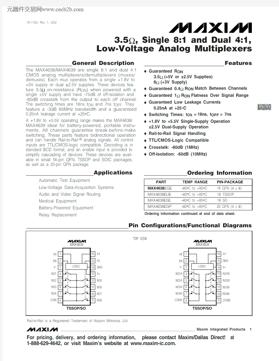
Pin Configurations/Functional Diagrams
For pricing, delivery, and ordering information,please contact Maxim/Dallas Direct!at 1-888-629-4642, or visit Maxim’s website at https://www.doczj.com/doc/e15948148.html,.
Ordering Information continued at end of data sheet.
M A X 4638/M A X 4639
3.5?, Single 8:1 and Dual 4:1, Low-Voltage Analog Multiplexers
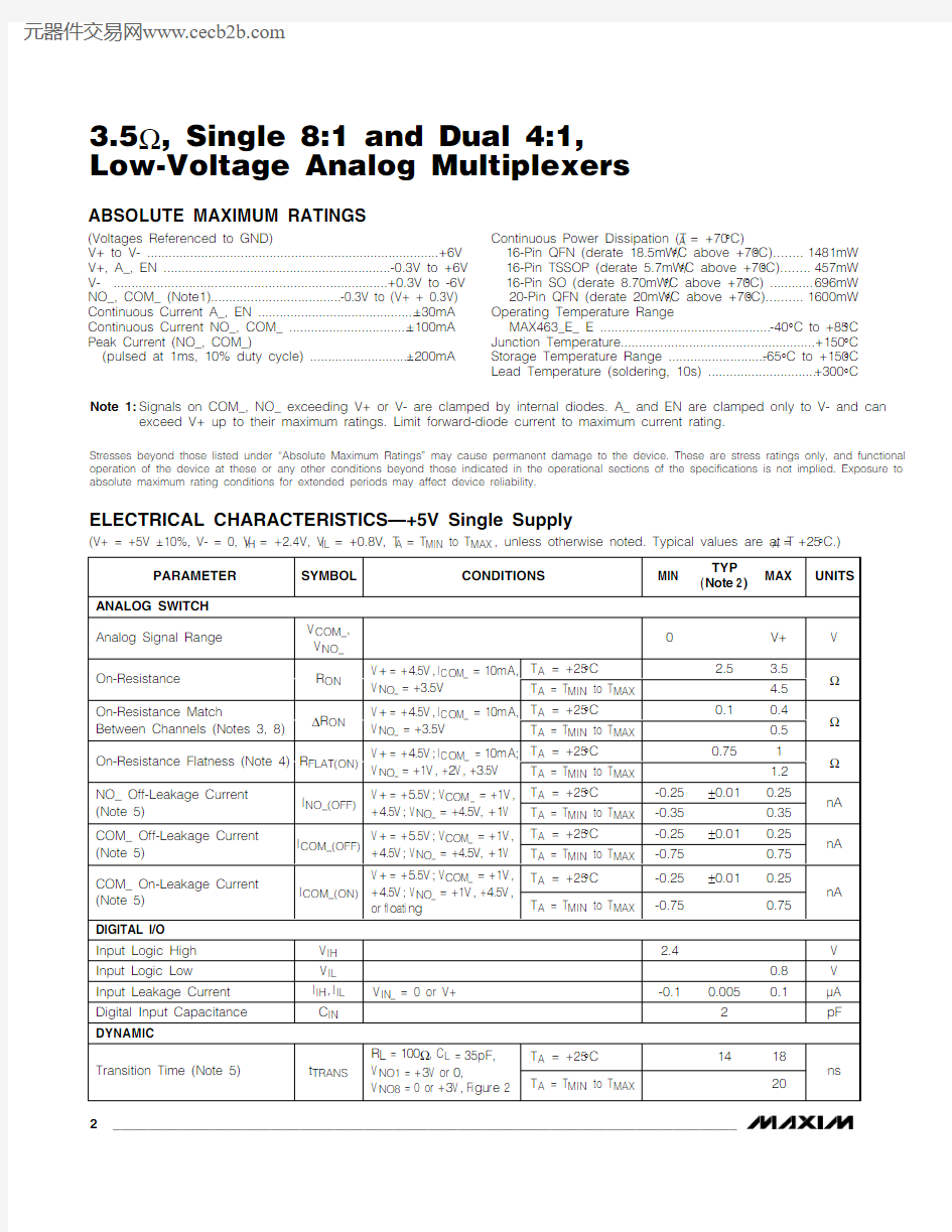
ABSOLUTE MAXIMUM RATINGS
ELECTRICAL CHARACTERISTICS—+5V Single Supply
(V+ = +5V ±10%, V- = 0, V IH = +2.4V, V IL = +0.8V, T A = T MIN to T MAX , unless otherwise noted. Typical values are at T A = +25°C.)
Stresses beyond those listed under “Absolute Maximum Ratings” may cause permanent damage to the device. These are stress ratings only, and functional operation of the device at these or any other conditions beyond those indicated in the operational sections of the specifications is not implied. Exposure to absolute maximum rating conditions for extended periods may affect device reliability.
(Voltages Referenced to GND)
V+ to V- .................................................................................+6V V+, A_, EN ...............................................................-0.3V to +6V V- ............................................................................+0.3V to -6V NO_, COM_ (Note1)....................................-0.3V to (V+ + 0.3V)Continuous Current A_, EN .............................................±30mA Continuous Current NO_, COM_ ..................................±100mA Peak Current (NO_, COM_)
(pulsed at 1ms, 10% duty cycle) ..............................±200mA
Continuous Power Dissipation (T A = +70°C)
16-Pin QFN (derate 18.5mW/°C above +70°C)........1481mW 16-Pin TSSOP (derate 5.7mW/°C above +70°C)........457mW 16-Pin SO (derate 8.70mW/°C above +70°C) ............696mW 20-Pin QFN (derate 20mW/°C above +70°C)..........1600mW Operating Temperature Range
MAX463_E_ E ...............................................-40°C to +85°C Junction Temperature......................................................+150°C Storage Temperature Range ...........................-65°C to +150°C Lead Temperature (soldering, 10s) ...............................+300°C
Note 1:Signals on COM_, NO_ exceeding V+ or V- are clamped by internal diodes. A_ and EN are clamped only to V- and can
exceed V+ up to their maximum ratings. Limit forward-diode current to maximum current rating.
MAX4638/MAX4639
3.5?, Single 8:1 and Dual 4:1, Low-Voltage Analog Multiplexers
_______________________________________________________________________________________3
ELECTRICAL CHARACTERISTICS —+5V Single Supply (continued)
(V+ = +5V ±10%, V- = 0, V IH = +2.4V, V IL = +0.8V, T A = T MIN to T MAX , unless otherwise noted. Typical values are at T A = +25°C.)
M A X 4638/M A X 4639
3.5?, Single 8:1 and Dual 4:1, Low-Voltage Analog Multiplexers 4_______________________________________________________________________________________
ELECTRICAL CHARACTERISTICS —+3.0V Single Supply
(V+ = +2.7V to +3.3V, V- = 0, V IH = +2.0V, V IL = +0.4V, T A = T MIN to T MAX , unless otherwise noted. Typical values are at V+ = +3V and T A = +25°C.)
MAX4638/MAX4639
3.5?, Single 8:1 and Dual 4:1, Low-Voltage Analog Multiplexers
ELECTRICAL CHARACTERISTICS —+3.0V Single Supply (continued)
(V+ = +2.7V to +3.3V, V- = 0, V IH = +2.0V, V IL = +0.4V, T A = T MIN to T MAX , unless otherwise noted. Typical values are at V+ = +3V and T A = +25°C.)
ELECTRICAL CHARACTERISTICS —±2.5V Dual Supplies
(V+ = +2.5 ±10%, V- = -2.5V ±10%, V IH = +2.0V, V IL = +0.4V, T A =T MIN to T MAX , unless otherwise noted. Typical values are at V±= ±2.5V and T A = +25°C.)
M A X 4638/M A X 4639
3.5?, Single 8:1 and Dual 4:1, Low-Voltage Analog Multiplexers
ELECTRICAL CHARACTERISTICS —±2.5V Dual Supplies (continued)
(V+ = +2.5 ±10%, V- = -2.5V ±10%, V IH = +2.0V, V IL = +0.4V, T A = T MIN to T MAX , unless otherwise noted. Typical values are at V±= ±2.5V and T A = +25°C.)
Note 3:?R ON = R ON(MAX)- R ON(MIN).
Note 4:Flatness is defined as the difference between the maximum and minimum value of on-resistance as measured over the
specified analog signal ranges.
Note 5:Guaranteed by design.
Note 6:Off-Isolation = 20log 10(V COM_/ V NO_), V COM_= output, V NO_= input to off switch.Note 7:Between any two switches.
Note 8:?R ON matching specifications for QFN packaged parts are guaranteed by design.
6______________________________________________________________________________________
MAX4638/MAX4639
3.5?, Single 8:1 and Dual 4:1, Low-Voltage Analog Multiplexers
_______________________________________________________________________________________7
05
10
15
20
25
2.0 2.51.0 1.50.5
3.0 3.5
4.0 4.5
5.0
ON-RESISTANCE vs. V COM
V COM (V)
R O N (?)
01.00.5
1.5
3.0
3.52.52.0
4.00
1.0 1.5
2.0 2.50.5
3.0 3.5
4.0 4.5
5.0
ON-RESISTANCE vs. V COM AND
TEMPERATURE
V COM (V)
R 0N (?)
2143
5
60 1.0 1.50.5 2.0 2.5 3.0
ON-RESISTANCE vs. V COM AND
TEMPERATURE
V COM (V)
R O N (?)
60
10080140120180160
2001.0 3.02.0 4.0 5.01.5 3.52.5 4.5 5.5 6.0
SUPPLY CURRENT vs. SUPPLY VOLTAGE
M A X 4638 t o c 04
SUPPLY VOLTAGE (V)
S U P P L Y C U R R
E N T (p A )
64
28101214161820-2.5
-0.5
1.5 3.5
CHARGE INJECTION vs. V COM
V COM (V)
C H A R G E (p C )
5.5
10
1
0.1
0.01
0.001
-40
10
-15
35
60
85
SUPPLY CURRENT vs. TEMPERATURE
M A X 463 t o c 06
TEMPERATURE (°C)
S U P P L Y C U R R E N T (n A )
0.6
0.81.0
1.21.41.61.81.8
2.8
2.3
3.3
3.8
4.3
4.8
5.3
LOGIC LEVEL THRESHOLD vs.SUPPLY VOLTAGE AND TEMPERATURE
SUPPLY VOLTAGE (V)
L O G I C V O L T A G E (V )
0105252015403530451.5
3.0
3.5
2.0
2.5
4.0
4.5
5.0
5.5
ENABLE TURN-ON/TURN-OFF TIME
vs. SUPPLY VOLTAGE
SUPPLY VOLTAGE (V)
T I M E (n s
)
246
810121416
-40
-15
10
35
60
85
ENABLE TURN-ON/TURN-OFF TIME
vs. TEMPERATURE
TEMPERATURE (°C)
T I M E (n s )
Typical Operating Characteristics
(V+ = +5V, V- = 0, T A = +25°C, unless otherwise noted.)
M A X 4638/M A X 4639
3.5?, Single 8:1 and Dual 4:1, Low-Voltage Analog Multiplexers -120
-80-100-40
-600-200.01
1
0.1
10
100
1000
FREQUENCY RESPONSE
FREQUENCY (MHz)
R E S P O N S E (d B )
0.010.001
10.1100101000-40
-20
20
40
80
60
ON/OFF-LEAKAGE CURRENT
vs. TEMPERATURE
TEMPERATURE (°C)
L E A K A G E C U R R E N T (p A
)
0.02
0.06
0.04
0.08
0.10
TOTAL HARMONIC DISTORTION
vs. FREQUENCY
FREQUENCY (kHz)
T H D (%)
0.01
1
0.1
10
100
Pin Description
Typical Operating Characteristics (continued)
(V+ = +5V, V- = 0, T A = +25°C, unless otherwise noted.)
MAX4638/MAX4639
3.5?, Single 8:1 and Dual 4:1, Low-Voltage Analog Multiplexers
_______________________________________________________________________________________9
Detailed Description
The MAX4638/MAX4639 are low-voltage, CMOS analog muxes. The MAX4638 is an 8:1 mux that switches one of eight inputs (NO1–NO8) to a common output (COM)as determined by the 3-bit binary inputs A0, A1, and A2. The MAX4639 is a 4:1 dual mux that switches one of four differential inputs to a common differential out-put as determined by the 2-bit binary inputs A0 and A1.Both the MAX4638/MAX4639 have an EN input that can be used to enable or disable the device. When dis-abled, all channels are switched off. See Truth Tables.
Applications Information
Overvoltage Protection
Proper power-supply sequencing is recommended for all CMOS devices. Do not exceed the absolute maxi-mum ratings because stresses beyond the listed rat-ings can cause permanent damage to the devices.Always sequence V+ on first, then V-, followed by the logic inputs. I f power-supply sequencing is not possi-ble, add two small-signal diodes (D1, D2) in series with the supply pins for overvoltage protection (Figure 1).Adding diodes reduces the analog signal range to one diode drop below V+ and one diode drop above V-, but does not affect the devices ’ low switch resistance.Device operation is unchanged, and the difference between V+ and V- should not exceed 6V. These pro-tection diodes are not recommended when using a sin-gle supply. For single-supply operation, V- should be connected to GND as close to the device as possible.
MAX4638 (Single 8-to-1 Mux)
MAX4639 (Dual 4-to-1 Mux)
Truth Tables
Ordering Information (continued)
M A X 4638/M A X 4639
3.5?, Single 8:1 and Dual 4:1, Low-Voltage Analog Multiplexers 10______________________________________________________________________________________
Test Circuits/Timing Diagrams
MAX4638/MAX4639
3.5?, Single 8:1 and Dual 4:1, Low-Voltage Analog Multiplexers
______________________________________________________________________________________11
Figure 5. Charge Injection
Test Circuits/Timing Diagrams (continued)
M A X 4638/M A X 4639
3.5?, Single 8:1 and Dual 4:1, Low-Voltage Analog Multiplexers 12______________________________________________________________________________________
Figure 7. Crosstalk
Figure 8. Channel OFF/ON Capacitance
Test Circuits/Timing Diagrams (continued)
Chip Information
TRANSISTOR COUNT: 632
Figure 6. Off-Isolation/On-Channel Bandwidth
MAX4638/MAX4639
3.5?, Single 8:1 and Dual 4:1, Low-Voltage Analog Multiplexers
______________________________________________________________________________________
13
Pin Configurations (continued)
M A X 4638/M A X 4639
3.5?, Single 8:1 and Dual 4:1, Low-Voltage Analog Multiplexers 14
______________________________________________________________________________________
Package Information
(The package drawing(s) in this data sheet may not reflect the most current specifications. For the latest package outline information,go to https://www.doczj.com/doc/e15948148.html,/packages .)
MAX4638/MAX4639
3.5?, Single 8:1 and Dual 4:1,
Low-Voltage Analog Multiplexers
Maxim cannot assume responsibility for use of any circuitry other than circuitry entirely embodied in a Maxim product. No circuit patent licenses are implied. Maxim reserves the right to change the circuitry and specifications without notice at any time.
Maxim Integrated Products, 120 San Gabriel Drive, Sunnyvale, CA 94086 408-737-7600_____________________15?2002 Maxim Integrated Products
Printed USA
is a registered trademark of Maxim Integrated Products.
Package Information (continued)
(The package drawing(s) in this data sheet may not reflect the most current specifications. For the latest package outline information,go to https://www.doczj.com/doc/e15948148.html,/packages .)