
MC74AC244, MC74ACT244Octal Buffer/Line Driver with 3-State Outputs
The MC74AC244/74ACT244 is an octal buffer and line driver designed to be employed as a memory address driver, clock driver and bus oriented transmitter/receiver which provides improved PC board density.
?3–State Outputs Drive Bus Lines or Buffer Memory Address Registers
?Outputs Source/Sink 24 mA
?
′ACT244 Has TTL Compatible Inputs
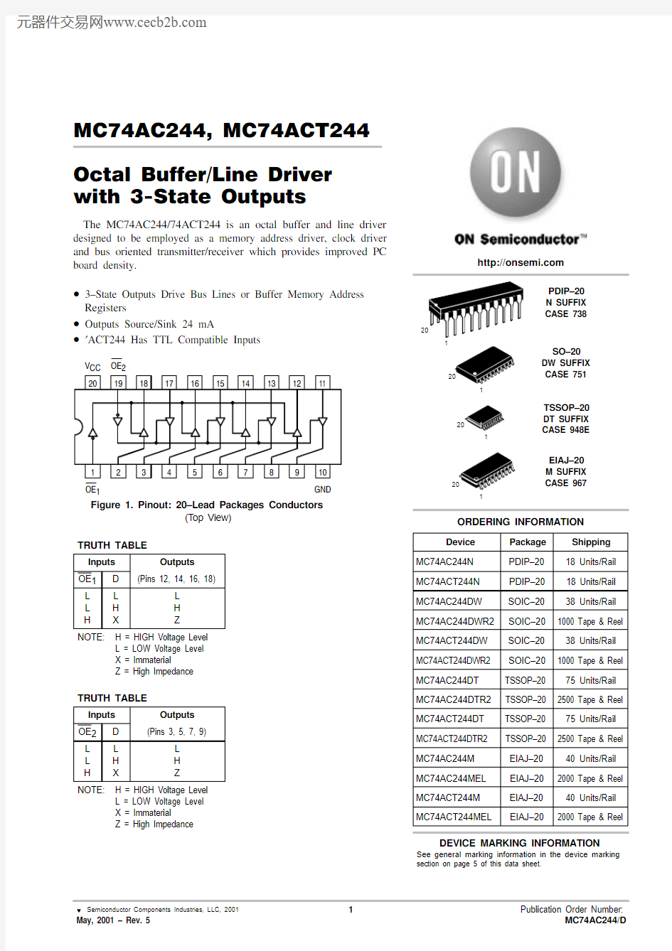
V OE OE 1
GND
Figure 1. Pinout: 20–Lead Packages Conductors
(Top View)
NOTE:
H = HIGH Voltage Level L = LOW Voltage Level X = Immaterial
Z = High Impedance
NOTE:
H = HIGH Voltage Level L = LOW Voltage Level X = Immaterial
Z = High Impedance
https://www.doczj.com/doc/ec4742830.html,
1
PDIP–20N SUFFIX
CASE 738
1
1
1
SO–20DW SUFFIX CASE 751
TSSOP–20DT SUFFIX CASE 948E EIAJ–20M SUFFIX CASE 967
Device
Package Shipping ORDERING INFORMATION
MC74AC244N PDIP–2018 Units/Rail MC74ACT244N PDIP–2018 Units/Rail MC74AC244DW SOIC–2038 Units/Rail MC74AC244DWR2SOIC–201000 T ape & Reel MC74ACT244DW SOIC–2038 Units/Rail MC74ACT244DWR2SOIC–201000 T ape & Reel MC74AC244DT TSSOP–2075 Units/Rail MC74AC244DTR2
TSSOP–202500 T ape & Reel MC74ACT244DT TSSOP–2075 Units/Rail MC74ACT244DTR2TSSOP–202500 T ape & Reel MC74AC244M EIAJ–2040 Units/Rail MC74AC244MEL EIAJ–202000 T ape & Reel MC74ACT244M EIAJ–2040 Units/Rail MC74ACT244MEL
EIAJ–20
2000 T ape & Reel
See general marking information in the device marking section on page 5 of this data sheet.
DEVICE MARKING INFORMATION
*Maximum Ratings are those values beyond which damage to the device may occur. Functional operation should be restricted to the Recom-mended Operating Conditions.
1.V IN from 30% to 70% V CC; see individual Data Sheets for devices that differ from the typical input rise and fall times.
2.V IN from 0.8 V to 2.0 V; see individual Data Sheets for devices that differ from the typical input rise and fall times.
*All outputs loaded; thresholds on input associated with output under test.
?Maximum test duration 2.0 ms, one output loaded at a time.
NOTE:I IN and I CC @ 3.0 V are guaranteed to be less than or equal to the respective limit @ 5.5 V V CC.
*Voltage Range 3.3 V is 3.3 V ±0.3 V.
*Voltage Range 5.0 V is 5.0 V ±0.5 V.
*All outputs loaded; thresholds on input associated with output under test.?Maximum test duration 2.0 ms, one output loaded at a time.
*Voltage Range 5.0 V is 5.0 V ±0.5 V.
AC 244ALYW
AC244AWLYYWW
MC74AC244N AWLYYWW
74AC244AWLYWW
MARKING DIAGRAMS
PDIP–20SO–20TSSOP–20
EIAJ–20
ACT 244ALYW
ACT244AWLYYWW
MC74ACT244N AWLYYWW
74ACT244AWLYWW
A = Assembly Location WL, L = Wafer Lot YY , Y = Year
WW, W = Work Week
PACKAGE DIMENSIONS
PDIP–20N SUFFIX
20 PIN PLASTIC DIP PACKAGE
CASE 738–03ISSUE E
NOTES:
1.DIMENSIONING AND TOLERANCING PER ANSI Y14.5M, 198
2.
2.CONTROLLING DIMENSION: INCH.
3.DIMENSION L TO CENTER OF LEAD WHEN FORMED PARALLEL.
4.DIMENSION B DOES NOT INCLUDE MOLD FLASH.
DIM MIN MAX MIN MAX MILLIMETERS
INCHES A 25.6627.171.010 1.070B 6.10 6.600.2400.260C 3.81 4.570.1500.180D 0.390.550.0150.022G 2.54 BSC 0.100 BSC J 0.210.380.0080.015K 2.80 3.550.1100.140L 7.62 BSC 0.300 BSC M 0 15 0 15 N
0.51 1.01
0.0200.040
____E 1.27 1.770.0500.070F 1.27 BSC 0.050 BSC SO–20DW SUFFIX
20 PIN PLASTIC SOIC PACKAGE
CASE 751D–05
ISSUE F
PACKAGE DIMENSIONS
TSSOP–20DT SUFFIX
20 PIN PLASTIC TSSOP PACKAGE
CASE 948E–02
ISSUE A
DIM A MIN MAX MIN MAX INCHES 6.600.260MILLIMETERS B 4.30 4.500.1690.177C 1.200.047
D 0.050.150.0020.006F 0.500.750.0200.030G 0.65 BSC 0.026 BSC H 0.270.370.0110.015J 0.090.200.0040.008J10.090.160.0040.006K 0.190.300.0070.012K10.190.250.0070.010L 6.40 BSC 0.252 BSC
M
0 8 0 8 ____
DIMENSIONING AND TOLERANCING PER
ANSI Y14.5M, 1982.
CONTROLLING DIMENSION: MILLIMETER.DIMENSION A DOES NOT INCLUDE MOLD
FLASH, PROTRUSIONS OR GATE BURRS. MOLD FLASH OR GATE BURRS SHALL NOT EXCEED 0.15 (0.006) PER SIDE.
DIMENSION B DOES NOT INCLUDE
INTERLEAD FLASH OR PROTRUSION.
INTERLEAD FLASH OR PROTRUSION SHALL NOT EXCEED 0.25 (0.010) PER SIDE.
DIMENSION K DOES NOT INCLUDE DAMBAR
PROTRUSION. ALLOWABLE DAMBAR
PROTRUSION SHALL BE 0.08 (0.003) TOTAL IN EXCESS OF THE K DIMENSION AT MAXIMUM MATERIAL CONDITION.
TERMINAL NUMBERS ARE SHOWN FOR
REFERENCE ONLY.
DIMENSION A AND B ARE TO BE
DETERMINED AT DATUM PLANE -W-.
6.400.252------EIAJ–20M SUFFIX
20 PIN PLASTIC EIAJ PACKAGE
CASE 967–01ISSUE O
DIM MIN MAX MIN MAX INCHES --- 2.05
---0.081
MILLIMETERS 0.050.200.0020.0080.350.500.0140.0200.180.270.0070.01112.3512.800.4860.5045.10
5.450.2010.2151.27 BSC 0.050 BSC 7.408.200.2910.3230.500.850.0200.0331.10 1.500.0430.0590 0.700.900.0280.035---0.81
---0.032
A 1H E Q 1L E _10 _0 _10 _NOTES:
??1.DIMENSIONING AND TOLERANCING PER
ANSI Y14.5M, 1982.
??2.CONTROLLING DIMENSION: MILLIMETER.??3.DIMENSIONS D AND E DO NOT INCLUDE
MOLD FLASH OR PROTRUSIONS AND ARE MEASURED AT THE PARTING LINE. MOLD
FLASH OR PROTRUSIONS SHALL NOT EXCEED 0.15 (0.006) PER SIDE.
??4.TERMINAL NUMBERS ARE SHOWN FOR
REFERENCE ONLY.
??5.THE LEAD WIDTH DIMENSION (b) DOES NOT
INCLUDE DAMBAR PROTRUSION. ALLOWABLE DAMBAR PROTRUSION SHALL BE 0.08 (0.003)TOTAL IN EXCESS OF THE LEAD WIDTH DIMENSION AT MAXIMUM MATERIAL
CONDITION. DAMBAR CANNOT BE LOCATED ON THE LOWER RADIUS OR THE FOOT. MINIMUM SPACE BETWEEN PROTRUSIONS AND ADJACENT LEAD TO BE 0.46 ( 0.018).
A b c D E e L M Z
ON Semiconductor and are trademarks of Semiconductor Components Industries, LLC (SCILLC). SCILLC reserves the right to make changes without further notice to any products herein. SCILLC makes no warranty, representation or guarantee regarding the suitability of its products for any particular purpose, nor does SCILLC assume any liability arising out of the application or use of any product or circuit, and specifically disclaims any and all liability, including without limitation special, consequential or incidental damages. “Typical” parameters which may be provided in SCILLC data sheets and/or specifications can and do vary in different applications and actual performance may vary over time. All operating parameters, including “Typicals” must be validated for each customer application by customer’s technical experts. SCILLC does not convey any license under its patent rights nor the rights of others.
SCILLC products are not designed, intended, or authorized for use as components in systems intended for surgical implant into the body, or other applications intended to support or sustain life, or for any other application in which the failure of the SCILLC product could create a situation where personal injury or death may occur. Should Buyer purchase or use SCILLC products for any such unintended or unauthorized application, Buyer shall indemnify and hold SCILLC and its officers, employees, subsidiaries, affiliates, and distributors harmless against all claims, costs, damages, and expenses, and reasonable attorney fees arising out of, directly or indirectly, any claim of personal injury or death associated with such unintended or unauthorized use, even if such claim alleges that SCILLC was negligent regarding the design or manufacture of the part. SCILLC is an Equal Opportunity/Affirmative Action Employer. PUBLICATION ORDERING INFORMATION
JAPAN: ON Semiconductor, Japan Customer Focus Center
4–32–1 Nishi–Gotanda, Shinagawa–ku, Tokyo, Japan 141–0031
Phone: 81–3–5740–2700
Email: r14525@https://www.doczj.com/doc/ec4742830.html,