Datasheet
R01DS0193EJ0100Rev.1.00Dec 10, 2012RL78/G12
RENESAS MCU
True Low Power Platform (as low as 63 μA/MHz), 1.8V to 5.5V operation, 2 to 16 Kbyte Flash, 31 DMIPS at 24MHz, for General Purpose Applications
1. OUTLINE
1.1 Features
Ultra-Low Power Technology
? 1.8V to 5.5V operation from a single supply
? Stop (RAM retained): 0.23μA, (LVD enabled): 0.31μA ? Snooze: 0.7mA (UART), 1.20mA (ADC) ? Operating: 63 μA /MHz
16-bit RL78 CPU Core
? Delivers 31 DMIPS at maximum operating frequency of 24MHz
? Instruction Execution: 86% of instructions can be executed in 1 to 2 clock cycles
? CISC Architecture (Harvard) with 3-stage pipeline ? Multiply Signed & Unsigned: 16 x 16 to 32-bit result in 1 clock cycle
? MAC: 16 x 16 to 32-bit result in 2 clock cycles
? 16-bit barrel shifter for shift & rotate in 1 clock cycle ? 1-wire on-chip debug function
Main Flash Memory
? Density: 2 KB to 16 KB ? Block size: 1KB
? On-chip single voltage flash memory with protection from block erase/writing
Data Flash Memory
? Data Flash with background operation ? Data flash size: 2 KB size options ? Erase Cycles: 1 Million (typ.)
? Erase/programming voltage: 1.8 V to 5.5 V
RAM
? 256 B to 1.5 KB size options
? Supports operands or instructions ? Back-up retention in all modes
High-speed Oscillator Oscillator
? 24MHz with +/- 1% accuracy over voltage (1.8 V to 5.5 V) and temperature (-40°C to 85°C)
? Pre-configured settings: 24MHz, 16MHz, 12MHz, 8MHz, 4MHz & 1MHz
Reset and Supply Management
? Power-on reset (POR) monitor/generator
? Low voltage detection (LVD) with 12 setting options (Interrupt and/or reset function)
Data Memory Access (DMA) Controller ? Up to 2 fully programmable channels ? Transfer unit: 8- or 16-bit
Multiple Communication Interfaces ? Up to 3 x I 2C master
? Up to 1 x I 2C multi-master ? Up to 3 x CSI/SPI (7-, 8-bit) ? Up to 3 x UART (7-, 8-, 9-bit)
Extended-Function Timers
? Multi-function 16-bit timers: Up to 8 channels ? Interval Timer: 12-bit, 1 channel
? 15 kHz watchdog timer : 1 channel (window function)
Rich Analog
? ADC: Up to 11 channels, 10-bit resolution, 2.1μs conversion time ? Supports 1.8V
? Internal voltage reference (1.45V) ? On-chip temperature sensor
Safety Features (IEC or UL 60730 compliance) ? Flash memory CRC calculation ? RAM parity error check ? RAM write protection ? SFR write protection
? Illegal memory access detection ? Clock stop/ frequency detection ? ADC self-test
General Purpose I/O
? 5V tolerant, high-current (up to 20mA per pin) ? Open-Drain, Internal Pull-up support
Operating Ambient Temperature ? Standard: –40°C to +85°C
Package Type and Pin Count ? QFN: 24
? SSOP: 20, 30
* There is difference in specifications between every product. Please refer to specification for details.
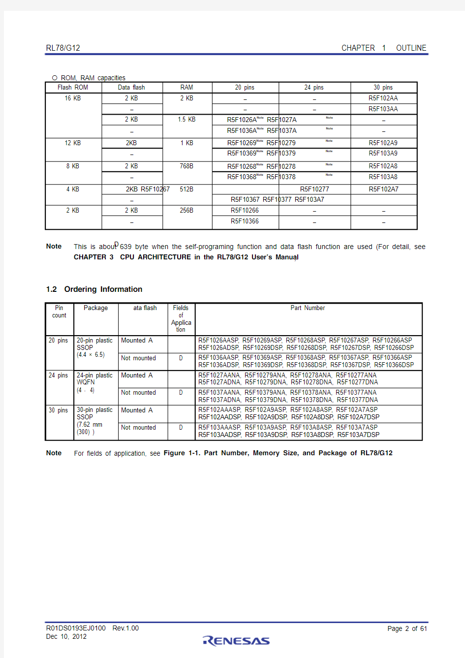
ROM, RAM capacities
Flash ROM Data flash RAM 20 pins 24 pins 30 pins 2 KB ? ? R5F102AA ? 2 KB
? ?
R5F103AA
2 KB R5F1026A Note R5F1027A Note ? 16 KB
?
1.5 KB R5F1036A Note
R5F1037A
Note
? 2KB R5F10269Note R5F10279Note R5F102A9 12 KB
?
1 KB R5F10369
Note
R5F10379Note
R5F103A9 2 KB R5F10268Note R5F10278Note R5F102A8 8 KB
?
768B R5F10368
Note
R5F10378
Note
R5F103A8
2KB R5F10267 R5F10277 R5F102A7
4 KB ? 512B R5F10367 R5F10377 R5F103A7 2 KB R5F10266 ? ? 2 KB
?
256B R5F10366
?
?
Note This is about 639 byte when the self-programing function and data flash function are used (For detail, see
CHAPTER 3 CPU ARCHITECTURE in the RL78/G12 User’s Manual ).
1.2 Ordering Information
Pin
count
Package D ata flash Fields of Applica tion
Part Number
Mounted A
R5F1026AASP, R5F10269ASP, R5F10268ASP, R5F10267ASP, R5F10266ASP R5F1026ADSP, R5F10269DSP, R5F10268DSP, R5F10267DSP, R5F10266DSP 20 pins 20-pin plastic SSOP (4.4 × 6.5) Not mounted D
R5F1036AASP, R5F10369ASP, R5F10368ASP, R5F10367ASP, R5F10366ASP R5F1036ADSP, R5F10369DSP, R5F10368DSP, R5F10367DSP, R5F10366DSP Mounted A
R5F1027AANA, R5F10279ANA, R5F10278ANA, R5F10277ANA R5F1027ADNA, R5F10279DNA, R5F10278DNA, R5F10277DNA 24 pins 24-pin plastic WQFN (4 × 4) Not mounted D
R5F1037AANA, R5F10379ANA, R5F10378ANA, R5F10377ANA R5F1037ADNA, R5F10379DNA, R5F10378DNA, R5F10377DNA Mounted A
R5F102AAASP, R5F102A9ASP, R5F102A8ASP, R5F102A7ASP R5F102AADSP, R5F102A9DSP, R5F102A8DSP, R5F102A7DSP 30 pins 30-pin plastic SSOP (7.62 mm (300) ) Not mounted D R5F103AAASP, R5F103A9ASP, R5F103A8ASP, R5F103A7ASP R5F103AADSP, R5F103A9DSP, R5F103A8DSP, R5F103A7DSP
Note
For fields of application, see Figure 1-1. Part Number, Memory Size, and Package of RL78/G12.
Figure 1-1. Part Number, Memory Size, and Package of RL78/G12
Part No. R 5 F 1 0 2 A A A x x x S P
Package type:
ROM number (Omitted with blank products)ROM capacity:
RL78/G12 group
Renesas MCU
Renesas semiconductor product
SP : SSOP, 0.65 mm pitch NA : WQFN, 0.50 mm pitch
6 : 2 KB
7 : 4 KB
8 : 8 KB
9
: 12 KB A : 16 KB
Pin count:
6 : 20-pin
7 : 24-pin A : 30-pin
Classification:
A : Consumer applications, operating ambient temperature : -40?C to 85?C D : Industrial applications, operating ambient temperature : -40?C to 85?C
Memory type:
F : Flash memory
102 : Data flash is povided
103 : Data flash is not provided
1.3 Differences between R5F102 and R5F103
The following are differences between the R5F102 and R5F103.
Whether the data flash memory is mounted or not
High-speed on-chip oscillator oscillation frequency accuracy
Number of channels in serial interface
Whether the DMA function is mounted or not
Whether the safety function is mounted or not
1.3.1 Data Flash
The data flash memory of 2 KB is mounted on the R5F102 but not on the R5F103.
Product Data Flash
2KB
R5F102
R5F1026A, R5F1027A, R5F102AA,
R5F10269, R5F10279, R5F102A9,
R5F10268, R5F10278, R5F102A8,
R5F10267, R5F10277, R5F102A7,
R5F10266 Note
Not mounted
R5F103
R5F1036A, R5F1037A, R5F103AA,
R5F10369, R5F10379, R5F103A9,
R5F10368, R5F10378 R5F103A8,
R5F10367, R5F10377, R5F103A7,
R5F10366
Note The RAM in the R5F10266 has capacity as small as 256 bytes. D epending on the customer’s program specification, the stack area to execute the data flash library may not be kept and data may not be written to or erased from the data flash memory.
Caution When the flash memory is rewritten via a user program, the flash ROM area and RAM area are used because each library is used. When using the library, refer to RL78 Family Flash Self Programming
Library Type01 User’s Manual and RL78 Family Data Flash Library Type04 User’s Manual.
1.3.2 On-chip oscillator characteristics
(1) High-speed on-chip oscillator oscillation frequency of the R5F102
Oscillator Condition
MIN MAX
Unit
T A = -20 to +85 °C -1
+1
High-speed on-chip
oscillator oscillation frequency accuracy T A = -40 to -20 °C -1.5+1.5
%
(2) High-speed on-chip oscillator oscillation frequency of the R5F103
Oscillator Condition
MIN MAX
Unit
High-speed on-chip oscillator oscillation frequency accuracy T A = -40 to + 85 °C -5
+5
%
1.3.3 Peripheral Functions
R5F102 R5F103
RL78/G12 20, 24 pin
product 30 pin product 20, 24 pin
product
30 pin product
UART 1 channel 3 channels 1 channel
CSI 2 channels 3 channels 1 channel Serial interface
Simplified I2C 2 channels 3 channels None DMA function 2 channels None
CRC operation Yes None
RAM guard Yes None Safety function
SFR guard Yes None
1.4 Pin Configuration (Top View)
1.4.1 20-pin products
? 20-pin plastic SSOP (4.4 × 6.5)
P21/ANI1/AV REFM P22/ANI2P23/ANI3
P10/ANI16/PCLBUZ0/SCK00/SCL00P11/ANI17/SI00/RxD0/SDA00 /TOOLRxD P12/ANI18/SO00/TxD0/TOOLTxD P13/ANI19/TI00/TO00/INTP2P14/ANI20/TI01/TO01/INTP3P61/KR5/SDAA0/(RxD0)P60/KR4/SCLA0/(TxD0)
P20/ANI0/AV REFP
P40/KR0/TOOL0
P137/INTP0
P122/KR2/X2/EXCLK/(TI02)/(INTP2)
P121/KR3/X1/(TI03)/(INTP3)
V SS V DD
P42/ANI21/SCK01/SCL01Note Note /TI03/TO03P41/ANI22/SO01/SDA01Note
Note /TI02/TO02/INTP1
P125/KR1/SI01/RESET Note Note
Note
Note Provided in the R5F102 products.
Remarks 1. For pin identification, see 1.5 Pin Identification .
2. Functions in parentheses in the above figure can be assigned via settings in the peripheral I/O redirection
register (PIOR).
? 24-pin plastic WQFN (4 × 4)
P40/KR0/TOOL0
P41/ANI22/SO01Note /SDA01Note /TI02/TO02/INTP1
P42/ANI21/SCK01Note /SCL01Note
/TI03/TO03P20/ANI0/AV REFP
P21/ANI1/AV REFM P22/ANI2
23/A N I 310/A N I 16/P C L B U Z 0/S C K 00/S C L 00N o t e
11/A N I 17/S I 00/R x D 0/S D A 00N o t e /T O O L R x D 12/A N I 18/S O 00/T x D 0/T O O L T x D 13/A N I 19/T I 00/T O 00/I N T P 214/A N I 20/T I 01/T O 01/I N T P 3
P 125/K R 1/S I 01N o t e /R E S E T P 137/I N T P 0P 122/K R 2/X 2/E X C L K /(T I 02)/(I N T P 2)P 121/K R 3/X 1/(T I 03)/(I N T P 3)V S S
V D D
Note
Note Note
Note Provided in the R5F102 products.
Remarks 1. For pin identification, see 1.5 Pin Identification .
2. Functions in parentheses in the above figure can be assigned via settings in the peripheral I/O redirection
register (PIOR).
? 30-pin plastic SSOP (7.62 mm (300))
P 21/ANI1/A V R E F M P 22/ANI2P 23/ANI3P 147/ANI18
P 10/S C K 00/S C L00Note /(TI07/T O07)
P 11/S I00/R xD0/T OOLR xD/S DA00Note /(TI06/T O06)P 12/S O00/TxD0/T OOL TxD/(TI05/T O05)P 13/TxD2Note /S O20Note /(S DAA0)/(TI04/T O04)
P14/RxD2Note /SI20Note /SDA20Note /(SCLA0) /(TI03/TO03)P15/PCLBUZ1/SCK20/SCL20/(TI02/TO02)P16/TI01/TO01/INTP5/(RxD0)P 17/TI02/T O02/(TxD0)P51/INTP2/SO11
P50/INTP1/SI11/SDA11P30/INTP3/SCK11/SCL11
P 20/ANI0/A V R E F P
P01/ANI16/TO00/RxD1P00/ANI17/TI00/TxD1
P120/ANI19P 40/T OOL0
R E S E T P 137/INTP 0P 122/X2/E XC LK
P 121/X1R E G C V S S V DD
P 60/S C LA0P 61/S DAA0
P 31/TI03/T O03/INTP 4/P C LB UZ0
Note Provided in the R5F102 products.
Caution Connect the REGC pin to V SS via capacitor (0.47 to 1 μF).
Remarks 1. For pin identification, see 1.5 Pin Identification . 2. Functions in parentheses in the above figure can be assigned via settings in the peripheral I/O redirection register (PIOR).
1.5 Pin Identification
ANI0 to ANI3, ANI16 to ANI22:
Analog input
REGC: RESET: Regulator Capacitance Reset AV REFM : Analog Reference Voltage Minus AV REFP :
Analog reference voltage plus
RxD0 to RxD2:
SCK00, SCK01, SCK11,
Receive Data
EXCLK: External Clock Input (Main System Clock)
SCK20:
SCL00, SCL01, SCL11, Serial Clock Input/Output
INTP0 to INTP5 Interrupt Request From Peripheral KR0 to KR9 Key Return SCL20, SCLA0: SDA00, SDA01, SDA11, Serial Clock Input/Output
P00 to P03: Port 0 SDA20, SDAA0: Serial Data Input/Output P10 to P17: Port 1 SI00, SI01, SI11, SI20: Serial Data Input P20 to P23: Port 2 SO00, SO01, SO11,
P30 to P31: Port 3 SO20: Serial Data Output P40 to P42: Port 4 TI00 to TI07: Timer Input P50, P51: Port 5 TO00 to TO07: Timer Output
P60, P61:
Port 6 TOOL0:
Data Input/Output for Tool P120 to P122, P125: Port 12 P137: Port 13 TOOLRxD, TOOLTxD:
Data Input/Output for External Device P147:
Port 14
TxD0 to TxD2: Transmit Data V DD :
Power supply
V SS : Ground
PCLBUZ0, PCLBUZ1:
Programmable Clock Output/ Buzzer Output
X1, X2:
Crystal Oscillator (Main System Clock)
1.6 Block Diagram
1.6.1 20-pin products
REFP
REFM Note Provided for the R5F102 products.
SCK00 SCK01 SCL00 SCL01
SCLA0 SDAA0REFP REFM
Note Provided for the R5F102 products.
10 to P 1720 to P 2340
120
C LB UZ0, P C LB UZ1
60, P 61121, P 122S C LA0
S DAA0
0 to INTP 5
00, P 01
V R E F P V R E F M 137
E G C
147
50, P 51
30, P 31R R S C S S C K S S S C S S C K S S R T S C S S C K S S TI02/T TI03/T T TI01/T (TI04/T (TI05/T (TI06/T (TI07/T
Note Provided for the R5F102 products.
Remark Functions in parentheses in the above figure can be assigned via settings in the peripheral I/O redirection
register (PIOR).
1.7 Outline of Functions
This outline describes the function at the time when Peripheral I/O redirection register (PIOR) is set to 00H (except timer output of R5F102Ax)
(1/2)
20-pin 24-pin 30-pin
Item
R5F1026x R5F1036x R5F1027x R5F1037x R5F102Ax R5F103Ax
Code flash memory 2 to 16 KB Note 1
4 to 16 KB
Data flash memory 2 KB
?
2 KB
?
2 KB
?
RAM
256 B to 1.5 KB 512 B to 1.5 KB
512 B to 2KB
Address space 1 MB
High-speed system clock
X1, X2 (crystal/ceramic) oscillation, external main system clock input (EXCLK) 1 to 20 MHz: V DD = 2.7 to 5.5 V, 1 to 8 MHz: V DD = 1.8 to 5.5 V
Main system clock
High-speed on-chip oscillator clock
HS (High-speed main) mode : 1 to 24 MHz (V DD = 2.7 to 5.5 V), 1 to 16 MHz (V DD = 2.4 to 5.5 V), LS (Low-speed main) mode : 1 to 8 MHz (V DD = 1.8 to 5.5 V) Low-speed on-chip oscillator clock 15 kHz (TYP)
General-purpose register
(8-bit register × 8) × 4 banks
0.04167 μs (High-speed on-chip oscillator clock: f IH = 24 MHz operation) Minimum instruction execution time
0.05 μs (High-speed system clock: f MX = 20 MHz operation)
Instruction set ? Data transfer (8/16 bits)
? Adder and subtractor/logical operation (8/16 bits) ? Multiplication (8 bits × 8 bits)
? Rotate, barrel shift, and bit manipulation (set, reset, test, and Boolean operation), etc.
Total 18 22 26 CMOS I/O 12 16 21 CMOS input 4
4 3
I/O port N-ch open-drain I/O (6 V tolerance)
2
16-bit timer 4 channels
8 channels
Watchdog timer 1 channel 12-bit Interval timer 1 channel
Timer Timer output
4/8
No te 2
(PWM Output
Note 3
: 3/7
Note 2
)
Notes 1. The self-programming function cannot be used in the R5F10266 and R5F10366. 2. When PIOR0 is set to 1 in R5F102Az.
3. The number of PWM outputs varies depending on the setting of channels in use (the number of masters and
slaves). (see 6.8.3 Operation as multiple PWM output function in the RL78/G12 User’s Manual ).
Caution When the flash memory is rewritten via a user program, the flash ROM area and RAM area are used because
each library is used. When using the library, refer to RL78 Family Flash Self Programming Library Type01 User’s Manual and RL78 Family Data Flash Library Type04 User’s Manual.
Note The illegal instruction is generated when instruction code FFH is executed.
Reset by the illegal instruction execution not issued by emulation with the in-circuit emulator or on-chip debug emulator.
2. ELECTRICAL SPECIFICATIONS
Cautions 1. The RL78/G12 has an on-chip debug function, which is provided for development and evaluation.
Do not use the on-chip debug function in products designated for mass production, because the
guaranteed number of rewritable times of the flash memory may be exceeded when this function is
used, and product reliability therefore cannot be guaranteed. Renesas Electronics is not liable for
problems occurring when the on-chip debug function is used.
2. The pins mounted depend on the product. Refer to 2.1 Port Function to 2.2.1 Functions for each
product in the RL78/G12 User’s Manual.
2.1 Absolute Maximum Ratings
Absolute Maximum Ratings (T A = 25°C)
Parameter Symbols
Conditions
Ratings Unit V DD ?0.5 to + 6.5 V Supply Voltage
V SS
?0.5 to + 0.3 V REGC terminal input
voltage Note 1
V IREGC REGC
?0.3 to +2.8 and ?0.3 to V DD + 0.3
Note 2
V
V I1 Other than P60, P61 ?0.3 to V DD + 0.3
Note 3
V
Input Voltage
V I2
P60, P61 (N-ch open drain) ?0.3 to 6.5 V
Output Voltage V O
?0.3 to V DD + 0.3Note 3
V
Analog input voltage
V AI
ANI0 to ANI22
?0.3 to V DD + 0.3
Note 3
and ?0.3 to
AVREF(+)+0.3
Note 3
V
Per pin Other than P20 to P23
?40 mA All the terminals other than P20 to P23?170 mA 20-, 24-pin products: P40 to P42 30-pin products: P00, P01, P40, P120 ?70 mA
I OH1
Total of
all pins
20-, 24-pin products: P00 to P03Note 4
,
P10 to P14
30-pin products: P10 to P17, P30, P31, P50, P51, P147
?100 mA
Per pin ?0.5 mA Output current, high
I OH2
Total of all pins
P20 to P23
?2 mA Per pin Other than P20 to P23
40 mA All the terminals other than P20 to P23170
mA
20-, 24-pin products: P40 to P42 30-pin products: P00, P01, P40, P12070 mA
I OL1
Total of all pins
20-, 24-pin products: P00 to P03, P10 to P14, P60, P61
30-pin products: P10 to P17, P30, P31, P50, P51, P60, P61, P147
100 mA
Per pin 1
mA
Output current, low
I OL2
Total of all pins
P20 to P23
5 mA Operating ambient temperature T A ?40 to +85 °C Storage temperature
T stg
?65 to +150
°C
Notes 1. 30-pin product only. 2. Connect the REGC pin to V SS via a capacitor (0.47 to 1 μF). This value determines the absolute maximum
rating of the REGC pin. Do not use it with voltage applied.
3. Must be 6.5 V or lower.
4. 24-pin product only.
Caution Product quality may suffer if the absolute maximum rating is exceeded even momentarily for any
parameter. That is, the absolute maximum ratings are rated values at which the product is on the verge of suffering physical damage, and therefore the product must be used under conditions that ensure that the absolute maximum ratings are not exceeded.
Remarks 1. Unless specified otherwise, the characteristics of alternate-function pins are the same as those of the port
pins.
2. AV REF (+) : + side reference voltage of the A/D converter.
2.2 Oscillator Characteristics
2.2.1 X1 clock oscillator characteristics
Note Indicates only oscillator characteristics. Refer to AC Characteristics for instruction execution time.
Cautions 1. When using the X1 oscillator, wire as follows in the area enclosed by the broken lines in the above figures to avoid an adverse effect from wiring capacitance.
? Keep the wiring length as short as possible.
? Do not cross the wiring with the other signal lines.
? Do not route the wiring near a signal line through which a high fluctuating current flows.
? Always make the ground point of the oscillator capacitor the same potential as V SS.
? Do not ground the capacitor to a ground pattern through which a high current flows.
? Do not fetch signals from the oscillator.
2. Since the CPU is started by the high-speed on-chip oscillator clock after a reset release, check the X1
clock oscillation stabilization time using the oscillation stabilization time counter status register
(OSTC) by the user. Determine the oscillation stabilization time of the OSTC register and the
oscillation stabilization time select register (OSTS) after sufficiently evaluating the oscillation
stabilization time with the resonator to be used.
2.2.2 On-chip oscillator characteristics
(T A = ?40 to +85°C, 1.8 V ≤ V DD≤ 5.5 V, V SS = 0 V)
Oscillators Parameters Conditions MIN.
TYP.
MAX.Unit
High-speed on-chip oscillator oscillation frequency Note 1f IH 1
24
MHz
T A = -20 to +85°C-1 +1 %
R5F102
T A = -40 to -20°C -1.5 +1.5%
High-speed on-chip oscillator
oscillation frequency
accuracy Note 2
R5F103 -5
+5 %
Low-speed on-chip oscillator
oscillation frequency
f IL15 kHz
Low-speed on-chip oscillator
oscillation frequency
accuracy
-15 +15%
Notes 1. High-speed on-chip oscillator frequency is selected by bits 0 to 3 of option byte (000C2H/010C2H) and bits
0 to 2 of HOCODIV register.
2.
This only indicates the oscillator characteristics. Refer to AC Characteristics for instruction execution time.
2.3 DC Characteristics
2.3.1 Pin characteristics
(T A = ?40 to +85°C, 1.8 V ≤ V DD ≤ 5.5 V, V SS = 0 V)
(1/4)
Parameter Symbol
Conditions
MIN. TYP. MAX.Unit Per pin
20-, 24-pin products: P00 to P03
Note 3
,
P10 to P14, P40 to P42
30-pin products: P00, P01,
P10 to P17, P30, P31, P40, P50, P51, P120, P147
?10.0
mA
4.0 V ≤ V DD ≤
5.5 V ?30.0mA 2.7 V ≤ V DD < 4.0 V ?
6.0mA 20-, 24-pin products: P40 to P42
30-pin products: P00, P01, P40, P120 1.8 V ≤ V DD < 2.7 V ?4.5mA 4.0 V ≤ V DD ≤ 5.5 V ?80.0mA 2.7 V ≤ V DD < 4.0 V ?18.0mA 20-, 24-pin products: P00 to P03 Note 3
,
P10 to P14
30-pin products: P10 to P17, P30, P31, P50, P51, P147 1.8 V ≤ V DD < 2.7 V
?10.0
mA
I OH1
Total of all pins
Note 2
All the terminals
?100mA Per pin ?0.1mA Output current, high
Note 1
I OH2 Total of all pins
Note 2
P20 to P23
?0.4
mA
Notes 1. value of current at which the device operation is guaranteed even if the current flows from the V DD pin to an
output pin.
2. Specification under conditions where the duty factor is 70%. The output current value that has changed the duty ratio can be calculated with the following expression (when changing the duty factor from 70% to n%). ? Total output current of pins = (I OH × 0.7)/(n × 0.01)
Total output current of pins = (?10.0 × 0.7)/(50 × 0.01) = ?14.0 mA
However, the current that is allowed to flow into one pin does not vary depending on the duty factor. A current higher than the absolute maximum rating must not flow into one pin. 3. 24-pin products only.
Caution P10 to P12, P41 for 20-pin products, P01, P10 to P12, P41 for 24-pin products, and P00, P10 to P15,
P17, P50 for 30-pin products, do not output high level in N-ch open-drain mode.
Remark Unless specified otherwise, the characteristics of alternate-function pins are the same as those of the port
pins.
Parameter Symbol
Conditions
MIN. TYP. MAX.Unit
20-, 24-pin products: P00 to P03 Note 3
,
P10 to P14,
P40 to P42
30-pin products: P00, P01, P10 to P17, P30, P31, P40, P50, P51, P120, P147
20.0 mA
Per pin
P60, P61
15.0 mA 4.0 V ≤ V DD ≤ 5.5 V 60.0 mA 2.7 V ≤ V DD < 4.0 V 9.0 mA 20-, 24-pin products: P40 to P42 30-pin products: P00, P01, P40, P120 1.8 V ≤ V DD < 2.7 V 1.8 mA 4.0 V ≤ V DD ≤ 5.5 V 80.0 mA 2.7 V ≤ V DD < 4.0 V 27.0 mA 20-, 24-pin products: P00 to P03
Note 3
,
P10 to P14, P60, P6130-pin products: P10 to P17, P30, P31, P50, P51, P60, P61, P147 1.8 V ≤ V DD < 2.7 V
5.4
mA
I OL1 Total of all pins
Note 2
All the terminals
140 mA Per pin
0.4
mA
Output current, low
Note 1
I OL2
Total of all pins
Note 2
P20 to P23
1.6 mA
Notes 1. Value of current at which the device operation is guaranteed even if the current flows from an output pin to
the V SS pin.
2. Specification under conditions where the duty factor is 70%. The output current value that has changed the duty ratio can be calculated with the following expression (when changing the duty factor from 70% to n%). ? Total output current of pins = (I OL × 0.7)/(n × 0.01)
Total output current of pins = (10.0 × 0.7)/(50 × 0.01) = 14.0 mA
However, the current that is allowed to flow into one pin does not vary depending on the duty factor. A current higher than the absolute maximum rating must not flow into one pin. 3. 24-pin products only.
Remark Unless specified otherwise, the characteristics of alternate-function pins are the same as those of the port
pins.
Notes 1. 20, 24-pin products only.
24-pin products only.
2.
Caution The maximum value of V IH of pins P01, P10 to P12, P41, for 20-, 24-pin products and P00, P10 to P15, P17, P50 for 30-pin products is V DD even in N-ch open-drain mode.
High level is not output in the N-ch open-drain mode.
Remark Unless specified otherwise, the characteristics of alternate-function pins are the same as those of the port
pins.