nRF24LE1中文数据手册
- 格式:pdf
- 大小:1.84 MB
- 文档页数:98
奋斗版 STM32 开发板例程手册———NRF24L01+转 USB 虚拟串口实验NRF24L01+转 USB 虚拟串口实验实验平台:奋斗版STM32开发板Tiny 实验内容:板子通过USB加电后,先向串口1输出一串测试数据,然后USB被PC识 别出来,虚拟出一个串口号给这个USB设备,此时可以通过在PC端的串口助手类 软件选择该串口号。
进入串口软件界面,可以通过软件无线收发一帧长度最长 为32字节的数据。
该例程可以和V3及MINI板的NRF24L01 UCGUI例程配合使用。
预先需要掌握的知识 2.4G通信模块NRF24L01 1. 产品特性2.4GHz 全球开放ISM 频段,最大0dBm 发射功率,免许可证使用 支持六路通道的数据接收 低工作电压:1.9 1.9~3.6V 低电压工作 高速率:2Mbps,由于空中传输时间很短,极大的降低了无线传输中的碰撞现象(软件设置1Mbps或者2Mbps的空中传输速率) 多频点:125 频点,满足多点通信和跳频通信需要 超小型:内置2.4GHz天线,体积小巧,15x29mm(包括天线) 低功耗:当工作在应答模式通信时,快速的空中传输及启动时间,极大的降低了电流消耗。
低应用成本:NRF24L01 集成了所有与RF协议相关的高速信号处理部分,比如:自动重发丢失数据包和自动产生应答信号等, NRF24L01的SPI接口可以利用单片机的硬件SPI口连接或用单片机I/O口进行模拟,内部有FIFO可以与各种高低速微处理器接口, 便于使用低成本单片机。
便于开发:由于链路层完全集成在模块上,非常便于开发。
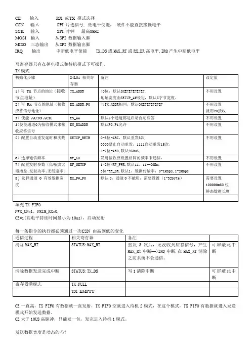
自动重发功能,自动检测和重发丢失的数据包,重发时间及重发次数可软件控制 自动存储未收到应答信号的数据包 自动应答功能,在收到有效数据后,模块自动发送应答信号,无须另行编程 载波检测—固定频率检测 内置硬件CRC 检错和点对多点通信地址控制 数据包传输错误计数器及载波检测功能可用于跳频设置 可同时设置六路接收通道地址,可有选择性的打开接收通道 标准插针Dip2.54MM 间距接口,便于嵌入式应用2.基本电气特性淘宝店铺:1奋斗版 STM32 开发板例程手册———NRF24L01+转 USB 虚拟串口实验3. 引脚定义:4.工作方式NRF2401有工作模式有四种: 收发模式 配置模式 空闲模式 关机模式 工作模式由CE 和寄存器内部PWR_UP、PRIM_RX 共同控制,见下表:淘宝店铺:2奋斗版 STM32 开发板例程手册———NRF24L01+转 USB 虚拟串口实验4.1 收发模式收发模式有Enhanced ShockBurstTM收发模式、ShockBurstTM收发模式和直接收发模式三种,收发模式由器件配置字决定,具体 配置将在器件配置部分详细介绍。
CE 输入RX 或TX 模式选择
CSN 输入SPI 片选信号, 低电平使能,硬件不能直接接低电平
SCK 输入SPI 时钟最高8MHZ
MOSI 输入从SPI 数据输入脚
MISO 三态输出从SPI 数据输出脚
IRQ 输出中断低电平使能 TX_DS或MAX_RT或RX_DR高电平,IRQ产生中断低电平
写寄存器只有在掉电模式和待机模式下可操作。
TX模式
填充TX FIFO
PWR_UP=1,PRIM_RX=0,
CE=1(高电平持续时间最小为10us),启动发射
每一条指令的执行都必须通过一次CSN 由高到低的变化
CE一直高,TX FIFO有数据就一直发射,TX FIFO空就进入待机2模式,在这个模式,TX FIFO有数据就进入发送模式开始发送数据。
CE大于10US高脉冲,只能发一包,发完进入待机1模式。
发送数据宽度是动态的吗?
PWR_UP=1,PRIM_RX=1,CE=1启动接收
CE=0进入待机模式1
载波检测cd,跳频,
发送模块没有成功发送数据时,发送端PLOS_CNT显示数据包丢失率太高时可将其设置位接收模式检测CD值如果CD为高说明通道出现了拥挤现象需要更改通信频道
时序
SPI指令,
F340
无线传32字节,是8位一组,4组,
STM32F103
一个8位,一个32位,如何通信
两个的FLASH地址位多了,
SPI接口几位,
如何送到FIFO
测试。
网上面关于多通道通信的好多资源都可以去共享,我也下了好多去调试,结果发现基本上都是调不通的。
其实这个归根到底还是一个地址匹配问题,通道0和1还好说,它是默认开启的,一般没问题,但通道2至5,通道如何匹配,数据手册上也只是说地址要匹配,到底要怎么做它没讲。
下面什么都不说了,直接上程序,这是用PIC16F877A来控制的,我会把要注意的重点标记出来,当然主要是多通道地址匹配的,其它的我就不多说了自己领悟。
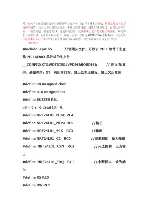
接收部分:#include <pic.h> //调用头文件,可以去PICC软件下去查找PIC16F88X单片机的头文件__CONFIG(XT&WDTDIS&LVPDIS&BORDIS); //定义配置字,晶振类型:XT,关闭开门狗,禁止低电压编程,禁止欠压复位#define u8 unsigned char#define u16 unsigned int#define BUZZER RB1u8 i=0,a=0,data[13]=0;#define NRF24L01_MISO RC4#define NRF24L01_MOSI RC5 //输出#define NRF24L01_SCK RC3 //输出#define NRF24L01_CE RC0 //使能控制设为输出#define NRF24L01_CSN RC2 //片选控制设为输出#define NRF24L01_IRQ RC1 //中断标志设为输入#define RS RE0#define RW RE1#define E RE2unsigned char SPIx_ReadWriteByte(unsigned char byte){unsigned char data;SSPBUF=byte;do{;}while(SSPIF==0);SSPIF=0;data=SSPBUF;return(data); // return read byte}//24L01操作线//#define NRF24L01_CE PAout(4) //24L01片选信号//#define NRF24L01_CSN PCout(4) //SPI片选信号//#define NRF24L01_IRQ PCin(5) //IRQ主机数据输入#define READ_REG 0x00 //读配置寄存器,低5位为寄存器地址#define WRITE_REG 0x20 //写配置寄存器,低5位为寄存器地址#define RD_RX_PLOAD 0x61 //读RX有效数据,1~32字节#define WR_TX_PLOAD 0xA0 //写TX有效数据,1~32字节#define FLUSH_TX 0xE1 //清除TX FIFO寄存器.发射模式下用#define FLUSH_RX 0xE2 //清除RX FIFO寄存器.接收模式下用#define REUSE_TX_PL 0xE3 //重新使用上一包数据,CE为高,数据包被不断发送.#define pop 0xFF //空操作,可以用来读状态寄存器//SPI(NRF24L01)寄存器地址#define CONFIG 0x00 //配置寄存器地址;bit0:1接收模式,0发射模式;bit1:电选择;bit2:CRC模式;bit3:CRC使能;//bit4:中断MAX_RT(达到最大重发次数中断)使能;bit5:中断TX_DS使能;bit6:中断RX_DR使能#define EN_AA 0x01 //使能自动应答功能bit0~5,对应通道0~5#define EN_RXADDR 0x02 //接收地址允许,bit0~5,对应通道0~5#define SETUP_AW 0x03 //设置地址宽度(所有数据通道):bit1,0:00,3字节;01,4字节;02,5字节;#define SETUP_RETR 0x04 //建立自动重发;bit3:0,自动重发计数器;bit7:4,自动重发延时250*x+86us#define RF_CH 0x05 //RF通道,bit6:0,工作通道频率;#define RF_SETUP 0x06 //RF寄存器;bit3:传输速率(0:1Mbps,1:2Mbps);bit2:1,发射功率;bit0:低噪声放大器增益#define STATUS 0x07 //状态寄存器;bit0:TX FIFO满标志;bit3:1,接收数据通道号(最大:6);bit4,达到最多次重发//bit5:数据发送完成中断;bit6:接收数据中断;#define MAX_TX 0x10 //达到最大发送次数中断#define TX_OK 0x20 //TX发送完成中断#define RX_OK 0x40 //接收到数据中断#define OBSERVE_TX 0x08 //发送检测寄存器,bit7:4,数据包丢失计数器;bit3:0,重发计数器#define CD 0x09 //载波检测寄存器,bit0,载波检测;#define RX_ADDR_P0 0x0A //数据通道0接收地址,最大长度5个字节,低字节在前#define RX_ADDR_P1 0x0B //数据通道1接收地址,最大长度5个字节,低字节在前#define RX_ADDR_P2 0x0C //数据通道2接收地址,最低字节可设置,高字节,必须同RX_ADDR_P1[39:8]相等;#define RX_ADDR_P3 0x0D //数据通道3接收地址,最低字节可设置,高字节,必须同RX_ADDR_P1[39:8]相等;#define RX_ADDR_P4 0x0E //数据通道4接收地址,最低字节可设置,高字节,必须同RX_ADDR_P1[39:8]相等;#define RX_ADDR_P5 0x0F //数据通道5接收地址,最低字节可设置,高字节,必须同RX_ADDR_P1[39:8]相等;#define TX_ADDR 0x10 //发送地址(低字节在前),ShockBurstTM模式下,RX_ADDR_P0与此地址相等#define RX_PW_P0 0x11 //接收数据通道0有效数据宽度(1~32字节),设置为0则非法#define RX_PW_P1 0x12 //接收数据通道1有效数据宽度(1~32字节),设置为0则非法#define RX_PW_P2 0x13 //接收数据通道2有效数据宽度(1~32字节),设置为0则非法#define RX_PW_P3 0x14 //接收数据通道3有效数据宽度(1~32字节),设置为0则非法#define RX_PW_P4 0x15 //接收数据通道4有效数据宽度(1~32字节),设置为0则非法#define RX_PW_P5 0x16 //接收数据通道5有效数据宽度(1~32字节),设置为0则非法#define FIFO_STATUS 0x17 //FIFO状态寄存器;bit0,RXFIFO寄存器空标志;bit1,RX FIFO满标志;bit2,3,保留//bit4,TX FIFO空标志;bit5,TX FIFO满标志;bit6,1,循环发送上一数据包.0,不循环;///////////////////////////////////////////////////// /////////////////////////////////////////24L01发送接收数据宽度定义#define TX_ADR_WIDTH 5 //5字节的地址宽度#define RX_ADR_WIDTH 5 //5字节的地址宽度#define TX_PLOAD_WIDTH 32 //20字节的用户数据宽度#define RX_PLOAD_WIDTH 32 //20字节的用户数据宽度void NRF24L01_Init(void);//初始化void RX_Mode(void);//配置为接收模式void TX_Mode(void);//配置为发送模式u8 NRF24L01_Write_Buf(u8 reg, u8 *pBuf, u8 u8s);//写数据区u8 NRF24L01_Read_Buf(u8 reg, u8 *pBuf, u8 u8s);//读数据区u8 NRF24L01_Read_Reg(u8 reg);//读寄存器u8 NRF24L01_Write_Reg(u8 reg, u8 value);//写寄存器u8 NRF24L01_Check(void);//检查24L01是否存在u8 NRF24L01_TxPacket(u8 *txbuf);//发送一个包的数据u8 NRF24L01_RxPacket(u8 *rxbuf);//接收一个包的数据const u8 TX_ADDRESS[TX_ADR_WIDTH]={0x34,0x43,0x10,0x10,0x0 1}; //本地发送地址const u8 RX_ADDRESS0[RX_ADR_WIDTH]={0x34,0x43,0x10,0x10,0 x01}; //接收0通道地址const u8 RX_ADDRESS1[RX_ADR_WIDTH]={0xc2,0xc2,0xc2,0xc2,0x c1}; //接收1通道地址const u8 RX_ADDRESS2[1]={0xb3}; //接收2通道地址const u8 RX_ADDRESS3[1]={0xa5}; //接收3通道地址const u8 RX_ADDRESS4[1]={0x35}; //接收4通道地址const u8 RX_ADDRESS5[1]={0x8f}; //接收5通道地址/********************************************/void delay1(unsigned char n){unsigned int m;for(;n>0;n--)for(m=0;m<100;m++){asm("NOP");}}void lcd_busy(){TRISD7=1; /*1602上DB7=1表明总线忙,同时RS=0 选择指令寄存器,RSS=1是选择数据寄存器*/RS=0;RW=1;E=1;while(RD7==1);E=0;TRISD7=0;}void lcd_write_commend(unsigned char u){lcd_busy();RS=0;RW=0;PORTD=u;E=1;asm("NOP");E=0;}void lcd_write_data(unsigned char k){lcd_busy();RS=1;RW=0;PORTD=k;E=1;asm("NOP");E=0;}void lcd_1602_ddram_add(u8 x,u8 y)//x是列,y是行,ddram是字符显示的地址{if(y==1){lcd_write_commend(0x80+x);}if(y==2){lcd_write_commend(0xc0+x);}}void lcd_disp(unsigned char x,unsigned char y,unsigned char l){x&=0x0f;//列地址限制在0-15y&=0x01;if(y==0x00)lcd_write_commend(x|0x80); //第一行的列地址写入elselcd_write_commend((x+0x40)|0x80); //第二行的列地址写入lcd_write_data(l+0x30);}void lcd_1602_display_shu(u8 num,u16 shu,u8 x,u8 y)//在液晶的任何位置显示五位内的数字{u8 wan,qian,bai,shi,ge;if(num>=1) ge=shu%10;if(num>=2) shi=shu%100/10;if(num>=3) bai=shu%1000/100;if(num>=4) qian=shu%10000/1000; if(num==5) wan=shu/10000;lcd_1602_ddram_add(x,y);if(num==1)lcd_write_data(ge|0x30);if(num==2){lcd_write_data(shi|0x30);lcd_write_data(ge|0x30);}if(num==3){lcd_write_data(bai|0x30);lcd_write_data(shi|0x30);lcd_write_data(ge|0x30);}if(num==4){lcd_write_data(qian|0x30);lcd_write_data(bai|0x30);lcd_write_data(shi|0x30);lcd_write_data(ge|0x30);}if(num==5){lcd_write_data(wan|0x30);lcd_write_data(qian|0x30);lcd_write_data(bai|0x30);lcd_write_data(shi|0x30);lcd_write_data(ge|0x30);}}void init_1602(){TRISD=0x00;TRISE=0x00;ADCON1=0X82;PORTE=0;PORTD=0;lcd_write_commend(0x38); /*这里的设置是更具需要,选择1602的各项配置,1602共有11条指令*/delay1(100);lcd_write_commend(0x38); /*这里的设置是更具需要,选择1602的各项配置,1602共有11条指令*/delay1(100);lcd_write_commend(0x38); /*这里的设置是更具需要,选择1602的各项配置,1602共有11条指令*/delay1(100);lcd_write_commend(0x38); //8位数据,双列,5*7字形lcd_write_commend(0x08);//显示功能关,无光标lcd_write_commend(0x01);//清屏指令lcd_write_commend(0x06);//写入新的数据后,光标右移,显示屏不移动lcd_write_commend(0x0c);//显示功能开,无光标,}/**********************汉字显示的代码******************************/const u8 hz1[]={0x1F,0x11,0x11,0x1F,0x11,0x11,0x11,0x1F};//日const u8 hz2[]={0x0F,0x09,0x0F,0x09,0x0F,0x09,0x09,0x13};//月const u8 hz3[]={0x04,0x0F,0x12,0x0F,0x0A,0x1F,0x02,0x02};//年const u8 hz4[]={0x1F,0x1F,0x04,0x04,0x04,0x04,0x1F,0x1F};//工const u8 hz5[]={0x0E,0x0A,0x0E,0x1F,0x04,0x07,0x03,0x01};//号void CGRAM(const u8 *hz,const u8 temp) //自定义字符存储{u8 i;for(i=0;i<8;i++){lcd_write_commend(temp+i);lcd_write_data(*(hz+i));}}/*******************************************///SPI写寄存器//reg:指定寄存器地址//value:写入的值u8 NRF24L01_Write_Reg(u8 reg,u8 value){u8 status;NRF24L01_CSN=0; //使能SPI传输status =SPIx_ReadWriteByte(reg);//发送寄存器号SPIx_ReadWriteByte(value); //写入寄存器的值NRF24L01_CSN=1; //禁止SPI传输return(status); //返回状态值}//读取SPI寄存器值//reg:要读的寄存器u8 NRF24L01_Read_Reg(u8 reg){u8 reg_val;NRF24L01_CSN = 0; //使能SPI传输SPIx_ReadWriteByte(reg); //发送寄存器号reg_val=SPIx_ReadWriteByte(0XFF);//读取寄存器内容NRF24L01_CSN = 1; //禁止SPI传输return(reg_val); //返回状态值}//在指定位置读出指定长度的数据//reg:寄存器(位置)//*pBuf:数据指针//len:数据长度//返回值,此次读到的状态寄存器值u8 NRF24L01_Read_Buf(u8 reg,u8 *pBuf,u8 len){u8 status,u8_ctr;NRF24L01_CSN = 0; //使能SPI传输status=SPIx_ReadWriteByte(reg);//发送寄存器值(位置),并读取状态值for(u8_ctr=0;u8_ctr<len;u8_ctr++)pBuf[u8_ctr]=SPIx_Rea dWriteByte(0XFF);//读出数据NRF24L01_CSN=1; //关闭SPI传输return status; //返回读到的状态值}//在指定位置写指定长度的数据//reg:寄存器(位置)//*pBuf:数据指针//len:数据长度//返回值,此次读到的状态寄存器值u8 NRF24L01_Write_Buf(u8 reg, u8 *pBuf, u8 len){u8 status,u8_ctr;NRF24L01_CSN = 0; //使能SPI传输status = SPIx_ReadWriteByte(reg);//发送寄存器值(位置),并读取状态值for(u8_ctr=0; u8_ctr<len; u8_ctr++)SPIx_ReadWriteByte(*pBuf++); //写入数据NRF24L01_CSN = 1; //关闭SPI传输return status; //返回读到的状态值}//启动NRF24L01发送一次数据//txbuf:待发送数据首地址//返回值:0,接收完成;其他,错误代码u8 NRF24L01_RxPacket(u8 *rxbuf){u8 sta;//SPIx_SetSpeed(SPI_SPEED_8); //spi速度为9Mhz (24L01的最大SPI时钟为10Mhz)sta=NRF24L01_Read_Reg(STATUS); //读取状态寄存器的值NRF24L01_Write_Reg(WRITE_REG+STATUS,sta); //清除TX_DS或MAX_RT中断标志if(sta&RX_OK)//接收到数据{NRF24L01_Read_Buf(RD_RX_PLOAD,rxbuf,RX_PLOAD_WID TH);//读取数据NRF24L01_Write_Reg(FLUSH_RX,0xff);//清除RX FIFO寄存器return 0;}return 1;//没收到任何数据}//该函数初始化NRF24L01到RX模式//设置RX地址,写RX数据宽度,选择RF频道,波特率和LNA HCURR //当CE变高后,即进入RX模式,并可以接收数据了void RX_Mode(void){NRF24L01_CE=0;NRF24L01_Write_Buf(WRITE_REG+RX_ADDR_P0,(u8*)TX_ ADDRESS,RX_ADR_WIDTH);//接收设备接收通道0使用和发送设备相同的发送地址NRF24L01_Write_Buf(WRITE_REG+RX_ADDR_P1,(u8*)RX_ ADDRESS1,RX_ADR_WIDTH);//接收设备接收通道1使用和发送设备相同的发送地址NRF24L01_Write_Buf(WRITE_REG+RX_ADDR_P2,(u8*)RX_ ADDRESS2,1);//接收设备接收通道2使用和发送设备相同的发送地址NRF24L01_Write_Buf(WRITE_REG+RX_ADDR_P3,(u8*)RX_ ADDRESS3,1);//接收设备接收通道3使用和发送设备相同的发送地址NRF24L01_Write_Buf(WRITE_REG+RX_ADDR_P4,(u8*)RX_ ADDRESS4,1);//接收设备接收通道4使用和发送设备相同的发送地址NRF24L01_Write_Buf(WRITE_REG+RX_ADDR_P5,(u8*)RX_ ADDRESS5,1);//接收设备接收通道5使用和发送设备相同的发送地址NRF24L01_Write_Reg(WRITE_REG+EN_AA,0x3f);//使能通道0到5的自动应答NRF24L01_Write_Reg(WRITE_REG+EN_RXADDR,0x3f);//使能通道0到5的接收地址NRF24L01_Write_Reg(WRITE_REG+RF_CH,40); //设置RF通信频率NRF24L01_Write_Reg(WRITE_REG+RX_PW_P0,RX_PLOAD_ WIDTH);//选择通道0的有效数据宽度NRF24L01_Write_Reg(WRITE_REG+RX_PW_P1,RX_PLOAD_ WIDTH);//选择通道1的有效数据宽度NRF24L01_Write_Reg(WRITE_REG+RX_PW_P2,RX_PLOAD_ WIDTH);//选择通道2的有效数据宽度NRF24L01_Write_Reg(WRITE_REG+RX_PW_P3,RX_PLOAD_ WIDTH);//选择通道3的有效数据宽度NRF24L01_Write_Reg(WRITE_REG+RX_PW_P4,RX_PLOAD_ WIDTH);//选择通道4的有效数据宽度NRF24L01_Write_Reg(WRITE_REG+RX_PW_P5,RX_PLOAD_ WIDTH);//选择通道5的有效数据宽度NRF24L01_Write_Reg(WRITE_REG+RF_SETUP,0x0f);//设置TX发射参数,0db增益,2Mbps,低噪声增益开启NRF24L01_Write_Reg(WRITE_REG+CONFIG, 0x0f);//配置基本工作模式的参数;PWR_UP,EN_CRC,16BIT_CRC,接收模式NRF24L01_CE = 1; //CE为高,进入接收模式}void delay(unsigned int m){unsigned int n;n=m;for(;n>0;n--)NOP();}void spi_init(){TRISC=0x13;SSPSTAT=0xc0;SSPCON=0x20;}void INT1(){TRISB=0x00;PORTB=0xfc;INTEDG = 1;INTF = 0;INTE = 1;GIE = 1;}void main(){u8 x=3;spi_init();init_1602();INT1();NRF24L01_CE=0;// chip enableNRF24L01_CSN=1;// Spi disable//NRF24L01_SCK=0;// Spi clock line init highCGRAM(hz1,0x40);CGRAM(hz2,0x48);CGRAM(hz3,0x50);CGRAM(hz4,0x58);CGRAM(hz5,0x60);//将这五个字写到1602用户自定义CGRAM中while(1){RX_Mode();NOP();if(NRF24L01_RxPacket(data)==0){lcd_write_commend(0x80);//第一行第一个字lcd_write_data(0x52);//显示接收的字母Rlcd_1602_display_shu(4,2013,x,1);//显示4位数的年份lcd_write_data(2); //显示汉字年lcd_1602_display_shu(2,8,x+5,1);//显示月份lcd_write_data(1); //显示汉字月lcd_1602_display_shu(2,7,x+8,1);//显示日期lcd_write_data(0); //显示汉字日lcd_write_commend(0xc0);//第二行显示lcd_write_data(3); //显示汉字工lcd_write_data(4); //显示汉字号lcd_write_commend(0xc0|0x02);//隔两格lcd_write_data(0x3A);//显示封号for(i=0;i<13;i++)//显示工人编号{lcd_disp(i+3,1,data[i]);}if(data[12]==1)RB0=1;elseRB0=0;}}}void interrupt ISR(void) {u16 y;if(INTF == 1){INTF = 0;asm("NOP");for(y=0;y<4000;y++){BUZZER=1;delay(20);BUZZER=0;}}}发送部分:#include <pic.h> //调用头文件,可以去PICC软件下去查找PIC16F88X单片机的头文件__CONFIG(XT&WDTDIS&LVPDIS&BORDIS); //定义配置字,晶振类型:XT,关闭开门狗,禁止低电压编程,禁止欠压复位#define u8 unsigned char#define u16 unsigned int#define key RB0u8 test[13]={2,0,1,2,5,8,0,8,0,2,1,5};u16 i=0;#define NRF24L01_MISO RC4#define NRF24L01_MOSI RC5 //输出#define NRF24L01_SCK RC3 //输出#define NRF24L01_CE RC0 //使能控制设为输出#define NRF24L01_CSN RC2 //片选控制设为输出#define NRF24L01_IRQ RC1 //中断标志设为输入*/#define RS RE0 //数据/命令选择#define RW RE1 //读/写选择#define E RE2 //使能信号unsigned char SPIx_ReadWriteByte(unsigned char byte){unsigned char data;SSPBUF=byte;do{;}while(SSPIF==0);SSPIF=0;data=SSPBUF;return(data); // return read byte}#define READ_REG 0x00 //读配置寄存器,低5位为寄存器地址#define WRITE_REG 0x20 //写配置寄存器,低5位为寄存器地址#define RD_RX_PLOAD 0x61 //读RX有效数据,1~32字节#define WR_TX_PLOAD 0xA0 //写TX有效数据,1~32字#define FLUSH_TX 0xE1 //清除TX FIFO寄存器.发射模式下用#define FLUSH_RX 0xE2 //清除RX FIFO寄存器.接收模式下用#define REUSE_TX_PL 0xE3 //重新使用上一包数据,CE为高,数据包被不断发送.#define pop 0xFF //空操作,可以用来读状态寄存器//SPI(NRF24L01)寄存器地址#define CONFIG 0x00 //配置寄存器地址;bit0:1接收模式,0发射模式;bit1:电选择;bit2:CRC模式;bit3:CRC使能;//bit4:中断MAX_RT(达到最大重发次数中断)使能;bit5:中断TX_DS使能;bit6:中断RX_DR使能#define EN_AA 0x01 //使能自动应答功能bit0~5,对应通道0~5#define EN_RXADDR 0x02 //接收地址允许,bit0~5,对应通道0~5#define SETUP_AW 0x03 //设置地址宽度(所有数据通道):bit1,0:00,3字节;01,4字节;02,5字节;#define SETUP_RETR 0x04 //建立自动重发;bit3:0,自动重发计数器;bit7:4,自动重发延时250*x+86us#define RF_CH 0x05 //RF通道,bit6:0,工作通道频#define RF_SETUP 0x06 //RF寄存器;bit3:传输速率(0:1Mbps,1:2Mbps);bit2:1,发射功率;bit0:低噪声放大器增益#define STATUS 0x07 //状态寄存器;bit0:TX FIFO满标志;bit3:1,接收数据通道号(最大:6);bit4,达到最多次重发//bit5:数据发送完成中断;bit6:接收数据中断;#define MAX_TX 0x10 //达到最大发送次数中断#define TX_OK 0x20 //TX发送完成中断#define RX_OK 0x40 //接收到数据中断#define OBSERVE_TX 0x08 //发送检测寄存器,bit7:4,数据包丢失计数器;bit3:0,重发计数器#define CD 0x09 //载波检测寄存器,bit0,载波检测;#define RX_ADDR_P0 0x0A //数据通道0接收地址,最大长度5个字节,低字节在前#define RX_ADDR_P1 0x0B //数据通道1接收地址,最大长度5个字节,低字节在前#define RX_ADDR_P2 0x0C //数据通道2接收地址,最低字节可设置,高字节,必须同RX_ADDR_P1[39:8]相等;#define RX_ADDR_P3 0x0D //数据通道3接收地址,最低字节可设置,高字节,必须同RX_ADDR_P1[39:8]相等;#define RX_ADDR_P4 0x0E //数据通道4接收地址,最低字节可设置,高字节,必须同RX_ADDR_P1[39:8]相等;#define RX_ADDR_P5 0x0F //数据通道5接收地址,最低字节可设置,高字节,必须同RX_ADDR_P1[39:8]相等;#define TX_ADDR 0x10 //发送地址(低字节在前),ShockBurstTM模式下,RX_ADDR_P0与此地址相等#define RX_PW_P0 0x11 //接收数据通道0有效数据宽度(1~32字节),设置为0则非法#define RX_PW_P1 0x12 //接收数据通道1有效数据宽度(1~32字节),设置为0则非法#define RX_PW_P2 0x13 //接收数据通道2有效数据宽度(1~32字节),设置为0则非法#define RX_PW_P3 0x14 //接收数据通道3有效数据宽度(1~32字节),设置为0则非法#define RX_PW_P4 0x15 //接收数据通道4有效数据宽度(1~32字节),设置为0则非法#define RX_PW_P5 0x16 //接收数据通道5有效数据宽度(1~32字节),设置为0则非法#define FIFO_STATUS 0x17 //FIFO状态寄存器;bit0,RX FIFO寄存器空标志;bit1,RX FIFO满标志;bit2,3,保留//bit4,TX FIFO空标志;bit5,TX FIFO满标志;bit6,1,循环发送上一数据包.0,不循环;///////////////////////////////////////////////////// ///////////////////////////////////////////////////////24L01发送接收数据宽度定义#define TX_ADR_WIDTH 5 //5字节的地址宽度#define RX_ADR_WIDTH 5 //5字节的地址宽度#define TX_PLOAD_WIDTH 32 //20字节的用户数据宽度#define RX_PLOAD_WIDTH 32 //20字节的用户数据宽度void NRF24L01_Init(void);//初始化void RX_Mode(void);//配置为接收模式void TX_Mode(void);//配置为发送模式u8 NRF24L01_Write_Buf(u8 reg, u8 *pBuf, u8 u8s);//写数据区u8 NRF24L01_Read_Buf(u8 reg, u8 *pBuf, u8 u8s);//读数据区u8 NRF24L01_Read_Reg(u8 reg);//读寄存器u8 NRF24L01_Write_Reg(u8 reg, u8 value);//写寄存器u8 NRF24L01_Check(void);//检查24L01是否存在u8 NRF24L01_TxPacket(u8 *txbuf);//发送一个包的数据u8 NRF24L01_RxPacket(u8 *rxbuf);//接收一个包的数据//下面这里就是重点啦,看看我用线条标出的是32位公用的地址,红色部分是低八位,注意位置啊啊啊啊啊啊const u8 TX_ADDRESS[TX_ADR_WIDTH]={0x35,0xc2,0xc2,0xc2,0xc 1}; //发送地址const u8 RX_ADDRESS0[RX_ADR_WIDTH]={0x35,0xc2,0xc2,0xc2,0x c1}; //接收3通道地址,就以通道3为例,其它都一个样//SPI写寄存器//reg:指定寄存器地址//value:写入的值u8 NRF24L01_Write_Reg(u8 reg,u8 value){u8 status;NRF24L01_CSN=0; //使能SPI传输status =SPIx_ReadWriteByte(reg);//发送寄存器号SPIx_ReadWriteByte(value); //写入寄存器的值NRF24L01_CSN=1; //禁止SPI传输return(status); //返回状态值}//读取SPI寄存器值//reg:要读的寄存器u8 NRF24L01_Read_Reg(u8 reg){u8 reg_val;NRF24L01_CSN = 0; //使能SPI传输SPIx_ReadWriteByte(reg); //发送寄存器号reg_val=SPIx_ReadWriteByte(0XFF);//读取寄存器内容NRF24L01_CSN = 1; //禁止SPI传输return(reg_val); //返回状态值}//在指定位置读出指定长度的数据//reg:寄存器(位置)//*pBuf:数据指针//len:数据长度//返回值,此次读到的状态寄存器值u8 NRF24L01_Read_Buf(u8 reg,u8 *pBuf,u8 len){u8 status,u8_ctr;NRF24L01_CSN =0; //使能SPI传输status=SPIx_ReadWriteByte(reg);//发送寄存器值(位置),并读取状态值for(u8_ctr=0;u8_ctr<len;u8_ctr++)pBuf[u8_ctr]=SPIx_ReadWriteByte(0XFF);//读出数据NRF24L01_CSN=1; //关闭SPI传输return status; //返回读到的状态值}//在指定位置写指定长度的数据//reg:寄存器(位置)//*pBuf:数据指针//len:数据长度//返回值,此次读到的状态寄存器值u8 NRF24L01_Write_Buf(u8 reg, u8 *pBuf, u8 len){u8 status,u8_ctr;NRF24L01_CSN = 0; //使能SPI传输status = SPIx_ReadWriteByte(reg);//发送寄存器值(位置),并读取状态值for(u8_ctr=0; u8_ctr<len; u8_ctr++)SPIx_ReadWriteByte(*pBuf++); //写入数据NRF24L01_CSN = 1; //关闭SPI传输return status; //返回读到的状态值}void delay(unsigned int n){for(;n>0;n--)NOP();}//启动NRF24L01发送一次数据//txbuf:待发送数据首地址//返回值:发送完成状况u8 NRF24L01_TxPacket(u8 *txbuf){u8 sta;//SPIx_SetSpeed(SPI_SPEED_8);//spi速度为9Mhz (24L01的最大SPI时钟为10Mhz)NRF24L01_CE=0; NRF24L01_IRQ=0;NRF24L01_Write_Buf(WR_TX_PLOAD,txbuf,TX_PLOAD_WID TH);//写数据到TX BUF 32个字节delay(5000);NRF24L01_CE=1;//启动发送delay(5000);while(NRF24L01_IRQ!=0);//等待发送完成sta=NRF24L01_Read_Reg(STATUS); //读取状态寄存器的值NRF24L01_Write_Reg(WRITE_REG+STATUS,sta); //清除TX_DS或MAX_RT中断标志if(sta&MAX_TX)//达到最大重发次数{NRF24L01_Write_Reg(FLUSH_TX,0xff);//清除TX FIFO寄存器return MAX_TX;}if(sta&TX_OK)//发送完成{return TX_OK;}elsereturn 0xff;//其他原因发送失败}//该函数初始化NRF24L01到TX模式//设置TX地址,写TX数据宽度,设置RX自动应答的地址,填充TX发送数据,选择RF频道,波特率和LNA HCURR//PWR_UP,CRC使能//当CE变高后,即进入RX模式,并可以接收数据了//CE为高大于10us,则启动发送.void TX_Mode(void){NRF24L01_CE=0;NRF24L01_Write_Buf(WRITE_REG+TX_ADDR,(u8*)TX_ADD RESS,TX_ADR_WIDTH);//写TX节点地址NRF24L01_Write_Buf(WRITE_REG+RX_ADDR_P0,(u8*)RX_ ADDRESS0,RX_ADR_WIDTH); //设置RX节点地址,主要为了使能ACK,TX_ADDRESS和RX_ADDRESS0一定要一致,不然就调不通的NRF24L01_Write_Reg(WRITE_REG+EN_AA,0x01);//使能通道0的自动应答NRF24L01_Write_Reg(WRITE_REG+EN_RXADDR,0x01); //使能通道0的接收地址NRF24L01_Write_Reg(WRITE_REG+SETUP_RETR,0x1a);//设置自动重发间隔时间:500us + 86us;最大自动重发次数:10次NRF24L01_Write_Reg(WRITE_REG+RF_CH,40);//设置RF通道为40NRF24L01_Write_Reg(WRITE_REG+RF_SETUP,0x0f); //设置TX发射参数,0db增益,2Mbps,低噪声增益开启NRF24L01_Write_Reg(WRITE_REG+CONFIG,0x0e);//配置基本工作模式的参数;PWR_UP,EN_CRC,16BIT_CRC,接收模式,开启所有中断NRF24L01_CE=1;//CE为高,10us后启动发送NOP();NOP();NOP();NOP();NOP();NOP();NOP();NOP();NOP();NOP();NOP();NOP();NOP();NOP();}void delay1(unsigned int n){unsigned int m;for(;n>0;n--)for(m=0;m<100;m++){asm("NOP");}}void read_1602_bz()//测忙{TRISD7=1;RS=0;RW=1;E=1;while(RD7==1);E=0;TRISD7=0;}void write_1602_dat(u8 data_1)//写数据{read_1602_bz();RS=1;RW=0;PORTD=data_1;delay(5);E=1;delay(5);E=0;}void write_1602_com(u8 com)//写指令{read_1602_bz();RS=0;RW=0;PORTD=com;delay(5);E=1;delay(5);E=0;}void lcd_1602_ddram_add(u8 x,u8 y)//x是列,y是行,ddram是字符显示的地址{if(y==1){write_1602_com(0x80+x);}if(y==2){write_1602_com(0xc0+x);}}void lcd_disp(unsigned char x,unsigned char y,unsigned charl){x&=0x0f;//列地址限制在0-15y&=0x01;if(y==0x00)write_1602_com(x|0x80); //第一行的列地址写入elsewrite_1602_com((x+0x40)|0x80); //第二行的列地址写入write_1602_dat(l+0x30);}void lcd_1602_display_shu(u8 num,u16 shu,u8 x,u8 y)//在液晶的任何位置显示五位内的数字{u8 wan,qian,bai,shi,ge;if(num>=1) ge=shu%10;if(num>=2) shi=shu%100/10;if(num>=3) bai=shu%1000/100;if(num>=4) qian=shu%10000/1000;if(num==5) wan=shu/10000;lcd_1602_ddram_add(x,y);if(num==1)if(num==2){write_1602_dat(shi|0x30); write_1602_dat(ge|0x30); }if(num==3){write_1602_dat(bai|0x30); write_1602_dat(shi|0x30); write_1602_dat(ge|0x30); }if(num==4){write_1602_dat(qian|0x30); write_1602_dat(bai|0x30); write_1602_dat(shi|0x30); write_1602_dat(ge|0x30); }if(num==5){write_1602_dat(wan|0x30);write_1602_dat(bai|0x30);write_1602_dat(shi|0x30);write_1602_dat(ge|0x30);}}/**********************汉字显示的代码******************************/const u8 hz1[]={0x1F,0x11,0x11,0x1F,0x11,0x11,0x11,0x1F};//日const u8 hz2[]={0x0F,0x09,0x0F,0x09,0x0F,0x09,0x09,0x13};//月const u8 hz3[]={0x04,0x0F,0x12,0x0F,0x0A,0x1F,0x02,0x02};//年void CGRAM(const u8 *hz,const u8 temp) //自定义字符存储{u8 i;for(i=0;i<8;i++){write_1602_com(temp+i);write_1602_dat(*(hz+i));}void init_1602(){TRISE=0x00;TRISD=0x00;//ADCON1=0X82;PCFG3=0;PCFG2=1;PCFG1=1;PCFG0=1; //A端口全部数字化PORTE=0;PORTD=0;write_1602_com(0x38);delay(50);write_1602_com(0x38);delay(50);write_1602_com(0x38);delay(50);write_1602_com(0x0c);write_1602_com(0x06);write_1602_com(0x01);void spi_init(){TRISC=0x13;SSPCON=0x20;SSPSTAT=0xc0;PIR1=0;}void main(){u8 x=3;TRISB0=0;spi_init();init_1602();CGRAM(hz1,0x40);CGRAM(hz2,0x48);CGRAM(hz3,0x50);//将这三个字写到1602用户自定义CGRAM中NRF24L01_CE=0; //使能24L01NRF24L01_CSN=1;//SPI片选取消SPIx_ReadWriteByte(0xff);//启动传输while(1){TX_Mode();if(key==0){delay(1);if(key==0)test[12]=1;}elsetest[12]=0;if(NRF24L01_TxPacket(test)==TX_OK){write_1602_com(0x80);//第一行第一个位置write_1602_dat(0x53);//显示发送的字母Slcd_1602_display_shu(4,2013,x,1);//显示4位数的年份write_1602_dat(2); //显示汉字年lcd_1602_display_shu(2,8,x+5,1);//显示月份write_1602_dat(1); //显示汉字月lcd_1602_display_shu(2,7,x+8,1);//显示日期write_1602_dat(0); //显示汉字日write_1602_com(0xc0);//第二行显示write_1602_dat(0x49); //显示字母Iwrite_1602_dat(0x44); //显示字母Dwrite_1602_com(0xc0|0x02);//隔两格write_1602_dat(0x3A);//显示封号for(i=0;i<13;i++)//显示工人编号{lcd_disp(i+3,1,test[i]);}}}}。
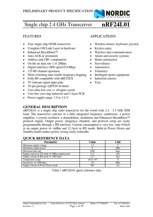
nRF24L01Single chip 2.4 GHz TransceiverFEATURES APPLICATIONS•True single chip GFSK transceiver •Wireless mouse, keyboard, joystick •Complete OSI Link Layer in hardware •Keyless entry•Enhanced ShockBurst™ •Wireless data communication•Auto ACK & retransmit •Alarm and security systems•Address and CRC computation •Home automation•On the air data rate 1 or 2Mbps •Surveillance•Digital interface (SPI) speed 0-8 Mbps •Automotive•125 RF channel operation •Telemetry•Short switching time enable frequency hopping •Intelligent sports equipment•Fully RF compatible with nRF24XX •Industrial sensors•5V tolerant signal input pads •Toys•20-pin package (QFN20 4x4mm)•Uses ultra low cost +/- 60 ppm crystal•Uses low cost chip inductors and 2-layer PCB•Power supply range: 1.9 to 3.6 VGENERAL DESCRIPTIONnRF24L01 is a single chip radio transceiver for the world wide 2.4 - 2.5 GHz ISMband. The transceiver consists of a fully integrated frequency synthesizer, a poweramplifier, a crystal oscillator, a demodulator, modulator and Enhanced ShockBurst™protocol engine. Output power, frequency channels, and protocol setup are easily programmable through a SPI interface. Current consumption is very low, only 9.0mAat an output power of -6dBm and 12.3mA in RX mode. Built-in Power Down andStandby modes makes power saving easily realizable.QUICK REFERENCE DATAUnit Parameter ValueMinimum supply voltage 1.9 VMaximum output power 0 dBmMaximum data rate 2000 kbpsSupply current in TX mode @ 0dBm output power 11.3 mASupply current in RX mode @ 2000 kbps 12.3 mATemperature range -40 to +85 °CSensitivity @ 1000 kbps -85 dBmSupply current in Power Down mode 900 nATable 1 nRF24L01 quick reference dataType NumberDescriptionVersionnRF24L01 20 pin QFN 4x4, RoHS & SS-00259 compliantD nRF24L01 IC Bare DiceD nRF24L01-EVKITEvaluation kit (2 test PCB, 2 configuration PCB, SW)1.0Table 2 nRF24L01 ordering informationBLOCK DIAGRAMDDD=0VD=0V=0VFigure 1 nRF24L01 with external components.PIN FUNCTIONSPin NamePin function Description1 CEDigital InputChip Enable Activates RX or TX mode2 CSN Digital InputSPI Chip Select 3SCK Digital InputSPI Clock4 MOSIDigital InputSPI Slave Data Input5 MISO Digital Output SPI Slave Data Output, with tri-state option6 IRQ Digital Output Maskable interrupt pin7 VDDPowerPower Supply (+3V DC) 8 VSS Power Ground (0V) 9 XC2 Analog Output Crystal Pin 2 10 XC1 Analog Input Crystal Pin 111 VDD_PA Power Output Power Supply (+1.8V) to Power Amplifier 12 ANT1 RF Antenna interface 1 13 ANT2 RFAntenna interface 2 14 VSS Power Ground (0V)15 VDD PowerPower Supply (+3V DC) 16 IREF Analog Input Reference current 17 VSS Power Ground (0V)18 VDD PowerPower Supply (+3V DC)19 DVDD Power Output Positive Digital Supply output for de-coupling purposes 20 VSSPowerGround (0V)Table 3 nRF24L01 pin functionPIN ASSIGNMENTVDDVSSANT2VSSCEVDD_PAANT1CSNMISO MOSI VDDIREFVSSIRQDVDDVSSXC2XC1VDDSCKFigure 2 nRF24L01 pin assignment (top view) for a QFN20 4x4 package.ELECTRICAL SPECIFICATIONSConditions: VDD = +3V, VSS = 0V, T A = - 40ºC to + 85ºCymbol Parameter (condition)NotesMin.Typ.Max. UnitsOperating conditionsVDD Supply voltage1.9 3.0 3.6 V TEMP Operating Temperature-40+27+85ºCDigital input pinV IH HIGH level input voltage 10.7VDD 5.25 VV IL LOW level input voltageVSS 0.3VDD VDigital output pinV OH HIGH level output voltage (I OH =-0.25m A ) VDD- 0.3 VDD VV OL LOW level output voltage (I OL =0.25m A) VSS 0.3 VGeneral RF conditionsf OP Operating frequency22400 2525 MHzf XTAL Crystal frequency16 MHz ∆f 1MFrequency deviation @ 1000kbps ±160 kHz ∆f 2MFrequency deviation @ 2000kbps ±320 kHz R GFSK Data rate ShockBurst™>0 2000 kbps F CHANNEL Channel spacing @ 1000kbps1 MHz F CHANNEL Channel spacing @ 2000kbps2 MHzTransmitter operationP RF Maximum Output Power30 +4 dBmP RFC RF Power Control Range 16 18 20 dB P RFCR RF Power A ccuracy ±4 dB P BW 20dB Bandwidth for Modulated Carrier(2000kbps)1800 2000 kHzP RF1 1st Adjacent Channel Transmit Power 2MHz -20 dBm P RF2 2nd Adjacent Channel Transmit Power 4MHz -50 dBm I VDD Supply current @ 0dBm output power 4 11.3 m AI VDD Supply current @ -18dBm output power 7.0m A I VDD Average Supply current @ -6dBm outputpower, Enhanced ShockBurst™50.05 m AI VDD Supply current in Standby-I mode 632 µA I VDD Supply current in power down900 nA1All digital inputs handle up to 5.25V signal inputs. Keep in mind that the VDD of the nRF24L01 must match theV IH of the driving device for output pins.2 Usable band is determined by local regulations 3Antenna load impedance = 15Ω+j88Ω 4Antenna load impedance = 15Ω+j88Ω. Effective data rate 1000kbps or 2000 kbps 5Antenna load impedance = 15Ω+j88Ω. Effective data rate 10kbps and full packets6Given for a 12pF crystal. Current when using external clock is dependent on signal swing.Receiver operationI VDD Supply current one channel 2000kbps 12.3 mAI VDD Supply current one channel 1000kbps 11.8 mARX SENS Sensitivity at 0.1%BER (@2000kbps) -82 dBm RX SENS Sensitivity at 0.1%BER (@1000kbps) -85 dBm C/I CO C/I Co-channel (@2000kbps) 778/119dB C/I1ST1st Adjacent Channel Selectivity C/I 2MHz 1/4 dB C/I2ND2nd Adjacent Channel Selectivity C/I 4MHz -21/-20 dB C/I3RD3rd Adjacent Channel Selectivity C/I 6MHz -27/-27 dB C/I CO C/I Co-channel (@1000kbps) 10911/1212dB C/I1ST1st Adjacent Channel Selectivity C/I 1MHz 8/8 dB C/I2ND2nd Adjacent Channel Selectivity C/I 2MHz -22/-21 dB C/I3RD3rd Adjacent Channel Selectivity C/I 3MHz -30/-30 dBTable 4 nRF24L01 RF specifications7Data rate is 2000kbps for the following C/I measurements8 According to ETSI EN 300 440-1 V1.3.1 (2001-09) page 279 nRF24L01 equal modulation on interfering signal10Data rate is 1000kbps for the following C/I measurements11 According to ETSI EN 300 440-1 V1.3.1 (2001-09) page 2712 nRF24L01 equal modulation on interfering signalPACKAGE OUTLINEnRF24L01 uses the QFN20 4x4 package, with matt tin plating.Package Type A A1 A3 K D/E e D2/E2 L L1 bSaw QFN20 (4x4 mm) MinTyp.Max0.800.850.950.000.020.050.20REF.0.20min4.0 BSC130.5 BSC2.502.602.700.350.400.450.15max0.180.250.30Figure 3 nRF24L01 Package Outline.13 BSC: Basic Spacing between Centers, ref. JEDEC standard 95, page 4.17-11/APackage marking:Abbreviations: B – Build Code, i.e. unique code for production sites, package type and test platform X – "X" grade, i.e. Engineering Samples (optional) YY – 2 digit Year number WW – 2 digit Week numberLL – 2 letter wafer lot number codeAbsolute Maximum RatingsSupply voltagesVDD............................- 0.3V to + 3.6V VSS..................................................0V Input voltageV I ..................................- 0.3V to 5.25V Output voltageV O .....................................VSS to VDDTotal Power DissipationP D (T A =85°C).............................60mWTemperaturesOperating Temperature…. - 40°C to + 85°C Storage Temperature….… - 40°C to + 125°CNote: Stress exceeding one or more of the limiting values may cause permanent damage to the device.ATTENTION!Electrostatic Sensitive Device Observe Precaution for handling.Glossary of Termsn R FB X2 4 L0 1 Y Y W W L LTerm DescriptionA CKAcknowledgementARTAutoRe-TransmitCE ChipEnableCLK ClockCRC Cyclic Redundancy CheckCSN ChipSelectNOTESB EnhancedShockBurst™ GFSK Gaussian Frequency Shift KeyingIRQ InterruptRequestISM Industrial-Scientific-Medical LNA LowNoiseAmplifierLSB Least Significant BitLSByte Least Significant ByteMbps Megabit per secondMCU Micro Controller UnitMISO Master In Slave OutMOSI Master Out Slave InMSB Most Significant BitMSByte Most Significant BytePCB Printed Circuit BoardPER Packet Error RatePID Packet Identity BitsPLD PayloadPRX PrimaryRXPTX PrimaryTXPWR_DWN PowerDownPWR_UP PowerUpRoHS Restriction of use of Certain Hazardous Substances RX ReceiveRX_DR Receive Data ReadySPI SerialPeripheralInterfaceTX TransmitTX_DS Transmit Data SentTable 5 GlossaryFUNCTIONAL DESCRIPTIONModes of operationThe nRF24L01 can be set in the following main modes depending on the level of the following primary I/Os and configuration registers:Mode PWR_UPregisterPRIM_RXregisterCE FIFOstateRX mode 1 1 1 -TX mode 1 0 1 Data in TX FIFOTX mode 1 0 1Î0 Stays in TX mode until packettransmission is finishedStandby-II 1 0 1 TX FIFO emptyStandby-I 1 - 0 No ongoing packet transmissionPower Down 0 - - -Table 6 nRF24L01 main modesAn overview of the nRF24L01 I/O pins in different modes is given in Table 7.Pin functions in the different modes of nRF24L01Pin Name Direction TX Mode RX Mode Standby Modes Power Down CE Input High Pulse >10µs High Low - CSN Input SPI Chip Select, active lowSCK Input SPIClock MOSI Input SPI Serial InputMISO Tri-stateOutputSPI Serial OutputIRQ Output Interrupt, active lowTable 7 Pin functions of the nRF24L01Standby ModesStandby-I mode is used to minimize average current consumption while maintaining short start up times. In this mode, part of the crystal oscillator is active. In Standby-II mode some extra clock buffers are active compared to Standby-I mode. Standby-II occurs when CE is held high on a PTX device with empty TX FIFO. The configuration word content is maintained during Standby modes. SPI interface may be activated. For start up time see Table 13.Power Down ModeIn power down nRF24L01 is disabled with minimal current consumption. When entering this mode the device is not active, but all registers values available from theSPI interface are maintained during power down and the SPI interface may be activated (CSN=0). For start up time see Table 13. The power down is controlled bythe PWR_UP bit in the CONFIG register.PRELIMINARY PRODUCT SPECIFICATIONnRF24L01 Single Chip 2.4 GHz Radio TransceiverPacket Handling MethodsnRF24L01 has the following Packet Handling Methods: • ShockBurst™ (compatible with nRF2401, nRF24E1, nRF2402 and nRF24E2 with 1Mbps data rate, see page 26) • Enhanced ShockBurst™ShockBurst™ShockBurst™ makes it possible to use the high data rate offered by nRF24L01 without the need of a costly, high-speed microcontroller (MCU) for data processing/clock recovery. By placing all high speed signal processing related to RF protocol on-chip, nRF24L01 offers the application microcontroller a simple SPI compatible interface, the data rate is decided by the interface-speed the micro controller itself sets up. By allowing the digital part of the application to run at low speed, while maximizing the data rate on the RF link, ShockBurst™ reduces the average current consumption in applications. In ShockBurst™ RX, IRQ notifies the MCU when a valid address and payload is received respectively. The MCU can then clock out the received payload from an nRF24L01 RX FIFO. In ShockBurst™ TX, nRF24L01 automatically generates preamble and CRC, see Table 12. IRQ notifies the MCU that the transmission is completed. All together, this means reduced memory demand in the MCU resulting in a low cost MCU, as well as reduced software development time. nRF24L01 has a three level deep RX FIFO (shared between 6 pipes) and a three level deep TX FIFO. The MCU can access the FIFOs at any time, in power down mode, in standby modes, and during RF packet transmission. This allows the slowest possible SPI interface compared to the average data-rate, and may enable usage of an MCU without hardware SPI.Enhanced ShockBurst™Enhanced ShockBurst™ is a packet handling method with functionality that makes bidirectional link protocol implementation easier and more efficient. In a typical bidirectional link, one will let the terminating part acknowledge received packets from the originating part in order to make it possible to detect data loss. Data loss can then be recovered by retransmission. The idea with Enhanced ShockBurst™ is to let nRF24L01 handle both acknowledgement of received packets and retransmissions of lost packets, without involvement from the microcontroller.Nordic Semiconductor ASA Revision: 1.2- Vestre Rosten 81, N-7075 Tiller, Norway-Phone +4772898900-Page 11 of 39Fax +4772898989 March 2006PRELIMINARY PRODUCT SPECIFICATIONnRF24L01 Single Chip 2.4 GHz Radio TransceiverTX3 TX2ipe 4P DataTX4 TX5Data PData PDa taTX1ipe 1PipeFigure 4: nRF24L01 in a star network configuration An nRF24L01 configured as primary RX (PRX) will be able to receive data trough 6 different data pipes, see Figure 4. A data pipe will have a unique address but share the same frequency channel. This means that up to 6 different nRF24L01 configured as primary TX (PTX) can communicate with one nRF24L01 configured as PRX, and the nRF24L01 configured as PRX will be able to distinguish between them. Data pipe 0 has a unique 40 bit configurable address. Each of data pipe 1-5 has an 8 bit unique address and shares the 32 most significant address bits. All data pipes can perform full Enhanced ShockBurst™ functionality. nRF24L01 will use the data pipe address when acknowledging a received packet. This means that nRF24L01 will transmit ACK with the same address as it receives payload at. In the PTX device data pipe 0 is used to received the acknowledgement, and therefore the receive address for data pipe 0 has to be equal to the transmit address to be able to receive the acknowledgement. See Figure 5 for addressing example.t Da a pe Pi 25Frequency Channel Nipe 3TX6Da 0 ipe ta PRXNordic Semiconductor ASA Revision: 1.2- Vestre Rosten 81, N-7075 Tiller, Norway-Phone +4772898900-Page 12 of 39Fax +4772898989 March 2006PRELIMINARY PRODUCT SPECIFICATIONnRF24L01 Single Chip 2.4 GHz Radio TransceiverFigure 5: Example on how the acknowledgement addressing is done An nRF24L01 configured as PTX with Enhanced ShockBurst™ enabled, will use the ShockBurst™ feature to send a packet whenever the microcontroller wants to. After the packet has been transmitted, nRF24L01 will switch on its receiver and expect an acknowledgement to arrive from the terminating part. If this acknowledgement fails to arrive, nRF24L01 will retransmit the same packet until it receives an acknowledgement or the number of retries exceeds the number of allowed retries given in the SETUP_RETR_ARC register. If the number of retries exceeds the number of allowed retries, this will be showed by the STATUS register bit MAX_RT which gives an interrupt. Whenever an acknowledgement is received by an nRF24L01 it will consider the last transmitted packet as delivered. It will then be cleared from the TX FIFO, and the TX_DS IRQ source will be set high. With Enhanced ShockBurst™ nRF24L01 offers the following benefits: • Highly reduced current consumption due to short time on air and sharp timing when operating with acknowledgement traffic • Lower system cost. Since the nRF24L01 handles all the high-speed link layer operations, like re-transmission of lost packet and generating acknowledgement to received packets, it is no need for hardware SPI on the system microcontroller to interface the nRF24L01. The interface can be done by using general purpose IO pins on a low cost microcontroller where the SPI is emulated in firmware. With the nRF24L01 this will be sufficient speed even when running a bi-directional link. • Greatly reduced risk of “on-air” collisions due to short time on air • Easier firmware development since the link layer is integrated on chipNordic Semiconductor ASA Revision: 1.2 - Vestre Rosten 81, N-7075 Tiller, Norway Phone +4772898900 -Page 13 of 39Fax +4772898989 March 2006PRELIMINARY PRODUCT SPECIFICATIONnRF24L01 Single Chip 2.4 GHz Radio TransceiverEnhanced ShockBurst™ Transmitting Payload:1. The configuration bit PRIM_RX has to be low. 2. When the application MCU has data to send, the address for receiving node (TX_ADDR) and payload data (TX_PLD) has to be clocked into nRF24L01 via the SPI interface. The width of TX-payload is counted from number of bytes written into the TX FIFO from the MCU. TX_PLD must be written continuously while holding CSN low. TX_ADDR does not have to be rewritten if it is unchanged from last transmit. If the PTX device shall receive acknowledge, data pipe 0 has to be configured to receive the acknowledgement. The receive address for data pipe 0 (RX_ADDR_P0) has to be equal to the transmit address (TX_ADDR) in the PTX device. For the example in Figure 5 the following address settings have to be performed for the TX5 device and the RX device: TX5 device: TX_ADDR = 0xB3B4B5B605 TX5 device: RX_ADDR_P0 = 0xB3B4B5B605 RX device: RX_ADDR_P5 = 0xB3B4B5B605 3. A high pulse on CE starts the transmission. The minimum pulse width on CE is 10 µs. 4. nRF24L01 ShockBurst™: • Radio is powered up • 16 MHz internal clock is started. • RF packet is completed (see the packet description) • Data is transmitted at high speed (1 Mbps or 2 Mbps configured by MCU). 5. If auto acknowledgement is activated (ENAA_P0=1) the radio goes into RX mode immediately. If a valid packet has been received in the valid acknowledgement time window, the transmission is considered a success. The TX_DS bit in the status register is set high and the payload is removed from TX FIFO. If a valid acknowledgement is not received in the specified time window, the payload is resent (if auto retransmit is enabled). If the auto retransmit counter (ARC_CNT) exceeds the programmed maximum limit (ARC), the MAX_RT bit in the status register is set high. The payload in TX FIFO is NOT removed. The IRQ pin will be active when MAX_RT or TX_DS is high. To turn off the IRQ pin, the interrupt source must be reset by writing to the status register (see Interrupt chapter). If no acknowledgement is received for a packet after the maximum number of retries, no further packets can be sent before the MAX_RX interrupt is cleared. The packet loss counter (PLOS_CNT) is incremented at each MAX_RT interrupt. I.e. ARC_CNT counts the number of retries that was required to get a single packet through. PLOS_CNT counts the number of packets that did not get through after maximum number of retries. 6. The device goes into Standby-I mode if CE is low. Otherwise next payload in TX FIFO will be sent. If TX FIFO is empty and CE is still high, the device will enter Standby-II mode. 7. If the device is in Standby-II mode, it will go to Standby-I mode immediately if CE is set low.Enhanced ShockBurstTM Receive Payload:1. RX is selected by setting the PRIM_RX bit in the configuration register to high. All data pipes that shall receive data must be enabled (EN_RXADDR register),Nordic Semiconductor ASA Revision: 1.2 - Vestre Rosten 81, N-7075 Tiller, Norway Phone +4772898900 Fax +4772898989 March 2006Page 14 of 39PRELIMINARY PRODUCT SPECIFICATIONnRF24L01 Single Chip 2.4 GHz Radio Transceiver2. 3. 4.5. 6. 7. 8.auto acknowledgement for all pipes running Enhanced ShockBurst™ has to be enabled (EN_AA register), and the correct payload widths must be set (RX_PW_Px registers). Addresses have to be set up as described in item 2 in the Enhanced ShockBurst™ transmit payload chapter above. Active RX mode is started by setting CE high. After 130µs nRF24L01 is monitoring the air for incoming communication. When a valid packet has been received (matching address and correct CRC), the payload is stored in the RX-FIFO, and the RX_DR bit in status register is set high. The IRQ pin will be active when RX_DR is high. RX_P_NO in status register will indicate what data pipe the payload has been received in. If auto acknowledgement is enabled, an acknowledgement is sent back. MCU sets the CE pin low to enter Standby-I mode (low current mode). MCU can clock out the payload data at a suitable rate via the SPI interface. The device is now ready for entering TX or RX mode or power down mode.Two way communication with payload in both directionsIf payload shall be sent in both directions, the PRIM_RX register must be toggled by redefining the device from PRX to PTX or vice versa. The controlling processors must handle the synchronicity between a PTX and a PRX. Data buffering in both RX FIFO and TX FIFO simultaneously is possible, but restricted to data pipes 1 to 5. The third level in TX FIFO shall only be written in RX, TX or Standby-II mode if data is stored in RX FIFOAuto Acknowledgement (RX)The auto acknowledgement function reduces the load of the external microcontroller, and may remove the need for dedicated SPI hardware in a mouse/keyboard or comparable systems, and hence reduce cost and average current consumption. Auto acknowledgement can be configured individually for each data pipe via the SPI interface. If auto acknowledgement is enabled and a valid packet (correct data pipe address and CRC) is received, the device will enter TX mode and send an acknowledgement packet. After the device has sent the acknowledgement packet, normal operation resumes, and the mode is determined by the PRIM_RX register and CE pin.Auto Re-Transmission (ART) (TX)An auto retransmission function is available. It will be used at the TX side in an auto acknowledgement system. In the SETUP_RETR register it will be possible to state how many times the data in the data register will be resent if data is not acknowledged. After each sending, the device will enter RX mode and wait a specified time period for acknowledgement. When the acknowledgement packet is received, the device will return to normal transmit function. If there is no more unsent data in the TX FIFO and the CE pin is low, the device will go into Standby-I mode. If the acknowledgement is not received, the device will go back to TX mode and resend the data. This will continue until acknowledgment is received, or a time out occursNordic Semiconductor ASA Revision: 1.2 - Vestre Rosten 81, N-7075 Tiller, Norway Phone +4772898900 Fax +4772898989 March 2006Page 15 of 39PRELIMINARY PRODUCT SPECIFICATIONnRF24L01 Single Chip 2.4 GHz Radio Transceiver(i.e. the maximum number of sending is reached). The only way to reset this is to set the PWR_UP bit low or let the auto retransmission finish. A packet loss counter will be incremented each time a packet does not succeed to reach the destination before time out. (Time out is indicated by the MAX_RT interrupt.) The packet loss counter is reset when writing to the RF channel register.Packet Identity (PID) and CRC used by Enhanced ShockBurstTMEach packet contains a two bit wide PID field to detect if the received packet is new or resent. The PID will prevent that the PRX device presents the same payload more than once to the microcontroller. This PID field is incremented at the TX side for each new packet received via the SPI interface. The PID and CRC field is used by the PRX device to determine whether a packet is resent or new. When several data is lost on the link, the PID fields may in some cases become equal to last received PID. If a packet has the same PID as the previous packet, nRF24L01 will compare the CRC sums from both packets. If they also are equal, the last received packet is considered as a copy of the previous and is discarded. 1: PRX device: The PRX device compares the received PID with the last PID. If the PID fields are different, the packet is considered to be new. If the PID is equal to last received PID, the received packet might be the same as last time. The receiver must check if the CRC is equal to the previous CRC. If the CRC is equal to the previous one, the packet is probably the same, and will be discarded. 2: PTX device: The transmitter increments the PID field each time it sends a new packet.TX side functionalityStartRX side functionalityStartNew packet from MCU?YesPID equal last PID?YesCRC equal last CRC?increment PID No No New packet is valid for MCUYes NoDiscard packet as a copyEndEndFigure 6 PID generation/detectionNordic Semiconductor ASA Revision: 1.2 - Vestre Rosten 81, N-7075 Tiller, Norway Phone +4772898900 Fax +4772898989 March 2006Page 16 of 39PRELIMINARY PRODUCT SPECIFICATIONnRF24L01 Single Chip 2.4 GHz Radio TransceiverThe length of the CRC is configurable through the SPI interface. It is important to notice that the CRC is calculated over the whole packet including address, PID and payload. No packet is accepted as correct if the CRC fails. This is an extra requirement for packet acceptance that is not illustrated in the figure above.Stationary Disturbance Detection – CDCarrier Detect (CD) is set high when an in-band RF signal is detected in RX mode, otherwise CD is low. The internal CD signal is filtered before presented to CD register. The internal CD signal must be high for at least 128µs. In Enhanced ShockBurst™ it is recommended to use the Carrier Detect functionality only when the PTX device does not succeed to get packets through, as indicated by the MAX_RT interrupt for single packets and by the packet loss counter (PLOS_CNT) if several packets are lost. If the PLOS_CNT in the PTX device indicates to high rate of packet losses, the device can be configured to a PRX device for a short time (Tstbt2a + CD-filter delay = 130µs+128µs = 258µs) to check CD. If CD was high (jam situation), the frequency channel should be changed. If CD was low (out of range), it may continue on the same frequency channel, but perform other adjustments. (A dummy write to the RF_CH will clear the PLOS_CNT.)Data PipesnRF24L01 configured as PRX can receive data addressed to 6 different data pipes in one physical frequency channel. Each data pipe has its own unique address and can be configured to have individual behavior. The data pipes are enabled with the bits in the EN_RXADDR register. By default only data pipe 0 and 1 are enabled. The address for each data pipe is configured in the RX_ADDR_Px registers. Always ensure that none of the data pipes have the exact same address. Data pipe 0 has a unique 40 bit configurable address. Data pipes 1-5 share the 32 most significant address bits and have only the LSByte unique for each data pipe. Figure 7 shows an example of how data pipes 0-5 are addressed. All pipes can have up to 40 bit address, but for pipe 1-5 only the LSByte is different, and the LSByte must be unique for all pipes.Nordic Semiconductor ASA Revision: 1.2- Vestre Rosten 81, N-7075 Tiller, Norway-Phone +4772898900-Page 17 of 39Fax +4772898989 March 2006PRELIMINARY PRODUCT SPECIFICATIONnRF24L01 Single Chip 2.4 GHz Radio TransceiverByte 4 Data pipe 0 (RX_ADDR_P0) Data pipe 1 (RX_ADDR_P1) Data pipe 2 (RX_ADDR_P2) Data pipe 3 (RX_ADDR_P3) Data pipe 4 (RX_ADDR_P4) Data pipe 5 (RX_ADDR_P5) 0xE7 0xC2 0xC2 0xC2 0xC2 0xC2 Byte 3 0xD3 0xC2 0xC2 0xC2 0xC2 0xC2 Byte 2 0xF0 0xC2 0xC2 0xC2 0xC2 0xC2 Byte 1 0x35 0xC2 0xC2 0xC2 0xC2 0xC2 Byte 0 0x77 0xC2 0xC3 0xC4 0xC5 0xC6Figure 7: Addressing data pipes 0-5 When a packet has been received at one of the data pipes and the data pipe is setup to generate acknowledgement, nRF24L01 will generate an acknowledgement with an address that equals the data pipe address where the packet was received. Some configuration settings are common to all data pipes and some are individual. The following settings are common to all data pipes: • CRC enabled/disabled (CRC always enabled when ESB is enabled) • CRC encoding scheme • RX address width • Frequency channel • RF data rate • LNA gain • RF output powerNordic Semiconductor ASA Revision: 1.2- Vestre Rosten 81, N-7075 Tiller, Norway-Phone +4772898900-Page 18 of 39Fax +4772898989 March 2006。
奋斗版 STM32 开发板例程手册———NRF24L01+转 USB 虚拟串口实验NRF24L01+转 USB 虚拟串口实验实验平台:奋斗版STM32开发板Tiny 实验内容:板子通过USB加电后,先向串口1输出一串测试数据,然后USB被PC识 别出来,虚拟出一个串口号给这个USB设备,此时可以通过在PC端的串口助手类 软件选择该串口号。
进入串口软件界面,可以通过软件无线收发一帧长度最长 为32字节的数据。
该例程可以和V3及MINI板的NRF24L01 UCGUI例程配合使用。
预先需要掌握的知识 2.4G通信模块NRF24L01 1. 产品特性2.4GHz 全球开放ISM 频段,最大0dBm 发射功率,免许可证使用 支持六路通道的数据接收 低工作电压:1.9 1.9~3.6V 低电压工作 高速率:2Mbps,由于空中传输时间很短,极大的降低了无线传输中的碰撞现象(软件设置1Mbps或者2Mbps的空中传输速率) 多频点:125 频点,满足多点通信和跳频通信需要 超小型:内置2.4GHz天线,体积小巧,15x29mm(包括天线) 低功耗:当工作在应答模式通信时,快速的空中传输及启动时间,极大的降低了电流消耗。
低应用成本:NRF24L01 集成了所有与RF协议相关的高速信号处理部分,比如:自动重发丢失数据包和自动产生应答信号等, NRF24L01的SPI接口可以利用单片机的硬件SPI口连接或用单片机I/O口进行模拟,内部有FIFO可以与各种高低速微处理器接口, 便于使用低成本单片机。
便于开发:由于链路层完全集成在模块上,非常便于开发。
自动重发功能,自动检测和重发丢失的数据包,重发时间及重发次数可软件控制 自动存储未收到应答信号的数据包 自动应答功能,在收到有效数据后,模块自动发送应答信号,无须另行编程 载波检测—固定频率检测 内置硬件CRC 检错和点对多点通信地址控制 数据包传输错误计数器及载波检测功能可用于跳频设置 可同时设置六路接收通道地址,可有选择性的打开接收通道 标准插针Dip2.54MM 间距接口,便于嵌入式应用2.基本电气特性淘宝店铺:1奋斗版 STM32 开发板例程手册———NRF24L01+转 USB 虚拟串口实验3. 引脚定义:4.工作方式NRF2401有工作模式有四种: 收发模式 配置模式 空闲模式 关机模式 工作模式由CE 和寄存器内部PWR_UP、PRIM_RX 共同控制,见下表:淘宝店铺:2奋斗版 STM32 开发板例程手册———NRF24L01+转 USB 虚拟串口实验4.1 收发模式收发模式有Enhanced ShockBurstTM收发模式、ShockBurstTM收发模式和直接收发模式三种,收发模式由器件配置字决定,具体 配置将在器件配置部分详细介绍。
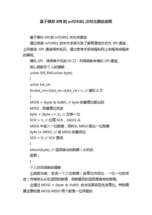
基于模拟SPI的nrf24l01点对点通信说明基于模拟SPI的nrf24l01点对点通信通过阅读nrf24l01的中文手册大致了解其通信方式为SPI通信,上网查询SPI通信相关知识。
通过参考手册例程和网上例程完成程序的编写。
模拟SPI:使用单片机的IO口,利用函数来模拟SPI通信。
核心函数及个人的理解:uchar SPI_RW(uchar byte){uchar bit_ctr;for(bit_ctr=0;bit_ctr<8;bit_ctr++) // 循环8次{MOSI = (byte & 0x80); // byte的最高位输出到MOSI,取最高位发送byte = (byte << 1); // 左移一位SCK = 1; // 拉高SCK,24L01从MOSI中读入一位数据,同时从MISO输出一位数据byte |= MISO; // 读MISO的最低位SCK = 0; // SCK置低}return(byte); // 返回读出的数据(从机的答复)}个人对该函数的理解:①函数功能:发送一个八位数据(由高位向低位,一位一位的发送)并接受从从机返回的数据,函数最后的返回是接受的数据。
②通过MOSI = (byte & 0x80); 的与运算实现先发高位。
特别需要注意的是MOSI MISO 两个都是一位传输的③发送一位数据后,数据左移右侧补0,接受到的一位数据与原先的数据进行或运算,将接受的数据放到最后一位而不影响原数据中尚未发送位上的数据。
如此八个循环后就实现了数据的发送和接受。
SPI_RW()函数理解后,程序中的其他函数都是实现nrf24l01的寄存器的配置,需参见数据手册进行理解(PS中文手册中有一些有错误,必要时可参见英文手册)。
具体的注释在我上发的程序中有详细的注释,请参见该程序。
基于模拟SPI的nrf24l01点对点通信,是nrf24l01 入门的应用,下一步工作我将继续研究基于硬件SPI的nrf24l01点对点通信,以及nrf24l01的点对多通信。
nRF24L01+单片机2.4 GHz收发器产品说明书v1.0主要功能:全球通用的2.4 GHz ISM波段操作250kbps, 1Mbps and 2Mbps空中数据传输速率超低功率运行发射功率为0dBm(1.0mW)时,发射电流为11.3mA2Mbps空中数据传输速率,接收电流为13.5mA掉电电流为900nA待机-I电流26μA片内电压调整器1.9至3.6V电源供电范围增强型ShockBurst TM自动数据包处理自动包数据包事务处理6数据通道的MultiCeiver TM与nRF24L01嵌入式兼容空中数据速率250kbps 和1Mbps,与nRF2401A,nRF2402, nRF24E1和nRF24E2兼容低BOM成本±60ppm 16MHz晶振容许5V输入紧凑的20引脚4x4mm QFN封装应用无线 PC外围设备鼠标,键盘和遥控器三和一桌面捆绑先进的媒体中心遥控器网络电话耳机游戏控制器蓝牙模块运动手表和传感器消费电子产品射频遥控器家庭和商业自动化超低功率无线传感器网络RFID 射频识别资产跟踪系统玩具免责条款北欧半导体ASA有权做出随时更改,提高产品可靠性、功能或设计,不另行通知。
北欧半导体ASA不承担由于应用程序或使用任何所述产品或电路引起的责任。
所有应用程序的信息咨询,不构成说明书的组成部分。
极限值超过一个或多个限制的应力可能会造成设备永久性损坏。
这些应力等级只有在这样或那样的操作环境中提出,在规范中没有给出。
长时间暴露在限制值附近可能会影响设备的可靠性。
生命支持应用这些产品并非为因故障会引起人身伤害的维生装备,设备或系统设计的。
北欧半导体ASA客户使用或出售这些产品,他们将自担风险并同意完全赔偿北欧半导体ASA因使用不当或销售行为造成任何损害。
详细联系方式访问www.nordicsemi.no进入北欧半导体销售办事处和全世界的分销商网站总办公室:Otto Nielsens vei 127004 Trondheim电话: +47 72 89 89 00传真: +47 72 89 89 89www.nordicsemi.no写作惯例本产品规范遵循一套排版规则,文档一致,容易阅读。
----E05-MLE132AP2E05-MLE132AP2是一款2.4GHz 无线模块,发射功率100mW,收发一体,自带高性能PCB 板载天线,也可选择IPEX 射频接口使用外置天线;目前已经多种场景中广泛应用。
该模块目前已经稳定量产,并适用于多种应用场景。
E05-MLE132AP2采用挪威Nordic 公司原装进口的nRF24LE1射频芯片设计开发,QFN32型,带有美国进口功率放大芯片;全进口工业级元器件,全无铅工艺,芯片内置51单片机,性能稳定,通信速率高,硬件的专业设计使模块可以插件或贴片,便于各种嵌入开发。
--*我司提供Altium designer封装库请前往官网下载或联系我们索取建议使用我公司专用底板E05-MLE132-T(点击产品型号可打开链接)进行软硬件开发,模块可以直接插于该底板之上。
此底板将模块所有GPIO引出,并提供USB-TTL串口,LED、用户按键、编程器接口等,便于用户加速产品开发。
编程下载软件YHTProgrammer.exe,该软件无需安装,可直接打开使用,用户可以选择芯片芯片,选择HEX文件,进行下载、读取、擦除、加密等多项操作。
界面如下:--E05-MLE132AP2E05-MLE124AP2nRF24LE1直插 2.4G201000SMA-K E05-MLE132A nRF24LE1直插 2.4G0100PCB E05-MLE132AP2nRF24LE1直插/贴片 2.4G201000PCB/IPEX★E05系列的所有型号无线模块经均可以互通★(EBYTE)是一家专业提供无线数传方案及产品的公司◆自主研发数百个型号的产品及软件;◆无线透传、WiFi、蓝牙、Zigbee、PKE、数传电台……等多系列无线产品;◆拥有近百名员工,数万家客户,累计销售产品数百万件;◆业务覆盖全球30多个国家与地区;◆通过了ISO9001质量管理体系、ISO14001环境体系认证;◆拥有多项专利与软件著作权,通过国际FCC/CE/ROHS等权威认证。
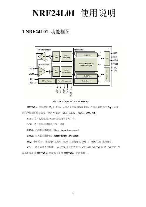
NRF24L01使用说明1 NRF24L01功能框图Fig.1 NRF24L01 BLOCK DIAGRAMNRF24L01的框图如 Fig.1所示,从单片机控制的角度来看,我们只需要关注 Fig.1右面的六个控制和数据信号,分别为 CSN、SCK、MISO、MOSI、IRQ、CE。
CSN:芯片的片选线,CSN为低电平芯片工作。
SCK:芯片控制的时钟线(SPI时钟)MISO:芯片控制数据线(Master input slave output)MOSI:芯片控制数据线(Master output slave input)IRQ:中断信号。
无线通信过程中 MCU主要是通过 IRQ与 NRF24L01进行通信。
CE:芯片的模式控制线。
在 CSN为低的情况下,CE协同 NRF24L01的 CONFIG寄存器共同决定 NRF24L01的状态(参照 NRF24L01的状态机)。
2 NRF24L01状态机NRF24L01的状态机见 Fig.2所示,对于 NRF24L01的固件编程工作主要是参照NRF24L01的状态机。
主要有以下几个状态Power Down Mode:掉电模式Tx Mode:发射模式Rx Mode:接收模式Standby-1Mode:待机1模式Standby-2 Mode:待机2模式上面五种模式之间的相互切换方法以及切换所需要的时间参照 Fig.2。
Fig.2 NRF24L01 State Machine对 24L01的固件编程的基本思路如下:1)置 CSN为低,使能芯片,配置芯片各个参数。
(过程见 3.Tx与 Rx的配置过程)配置参数在 Power Down状态中完成。
2)如果是 Tx模式,填充 Tx FIFO。
3)配置完成以后,通过 CE与 CONFIG中的 PWR_UP与 PRIM_RX参数确定 24L01 要切换到的状态。
Tx Mode:PWR_UP=1; PRIM_RX=0; CE=1 (保持超过 10us就可以);Rx Mode: PWR_UP=1; PRIM_RX=1; CE=1;4) IRQ引脚会在以下三种情况变低:Tx FIFO发完并且收到 ACK(使能 ACK情况下)Rx FIFO收到数据达到最大重发次数将 IRQ接到外部中断输入引脚,通过中断程序进行处理。
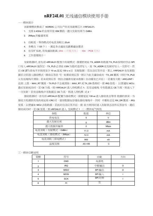
nRF24L01无线通信模块使用手册一、模块简介该射频模块集成了NORDIC公司生产的无线射频芯片I1RF24L01:1. 支持2.4GHz的全球开放ISM频段,最大发射功率为OdBm2. 2Mbps,传输速率高3. 功耗低,等待模式时电流消耗仅22uA4. 多频点(125个),满足多点通信及跳频通信需求5. 在空旷场地,有效通信距离:25m (外置天线)、10m (PCB天线)6. 工作原理简介:发射数据时,首先将nRF24L01配巻为发射模式,接着把地址TX_ADDR和数据TX_PLD 按照时序由SPI 口写入nRF24L01缓存区,TX_PLD必须在CSN为低时连续写入,而TX_ADDR在发射时写入一次即可,然后CE置为高电平并保持至少10 us,延迟130 u s后发射数据:若自动应答开启,那么I1RF24L01在发射数据后立即进入接收模式,接收应答信号。
如果收到应答,则认为此次通信成功,TX_DS置髙,同时TX_PLD 从发送堆栈中淸除: 若未收到应答,则自动重新发射该数据(自动重发已开启),若重发次数(ARCJ2NT)达到上限,MAX_RT置髙,TX.PLD不会被淸除;MAX_RT或TX_DS巻髙时,使IRQ变低,以便通知MCU.最后发射成功时,若CE为低,则I1RF24L01进入待机模式1:若发送堆栈中有数据且CE为髙,则进入下一次发射:若发送堆栈中无数据且CE为高,则进入待机模式2。
接收数据时,首先将nRF24L01配置为接收模式,接着延迟130 us进入接收状态等待数据的到来。
当接收方检测到有效的地址和CRC时,就将数据包存储在接收堆栈中,同时中断标志位RX_DR置高,IRQ 变低,以便通知MCU去取数据。
若此时自动应答开启,接收方则同时进入发射状态回传应答信号。
最后注:上图为示总连接,可根据自己实际需求进行更改:使用AT89S52MCU模块时,请将NH24L01通讯模块每个端口(MOSL SCK、CSN和CE)接4.7K的排阻上拉到VCC増强其驱动能力(如下图:)。

NRF24L01使用参考资料1、内部组成图
NRF24L01的状态:
Power Down Mode:掉电模式
Tx Mode:发射模式
Rx Mode:接收模式
Standby-1Mode:待机1模式
Standby-2Mode:待机2模式
2、NRF24L01的SPI读写时序:
3、编程基本思路:
拉低CSN,使能芯片,配置芯片各个参数。
配置参数在Power Down状态中完成。
如果是Tx模式,填充Tx FIFO。
配置完成后,通过CE与CONFIG中的PWR_UP与PRIM_RX参数确定24L01要切换的状态。
Tx Mode:PWR_UP=1;PRIM_RX=0;CE=1(保持超过10us就可以);
Rx Mode:PWR_UP=1;PRIM_RX=1;CE=1;
IRQ引脚会在以下三种情况变低:
Tx FIFO发完并且收到ACK(使能ACK情况下)
Rx FIFO收到数据
达到最大重发次数
将IRQ接到外部中断输入引脚,通过中断程序进行处理。
4、控制命令
命令字:由高位到低位(每字节)。
数据字节:低字节到高字节,每一字节高位在前。
5、相关寄存器地址宏定义
5、引脚功能
6、三个数据
7、管脚定义
8、设计参考图。
NRF24L01详细教程NRF24L01是一款低功耗2.4GHz无线收发模块,广泛应用于各种无线通信项目中。
它可以使微控制器与其他设备进行无线通信,例如Arduino 与Arduino之间的通信、Arduino与无线传感器节点的通信等。
下面是一个详细的NRF24L01教程。
1.NRF24L01的基本介绍NRF24L01是一款由Nordic Semiconductor公司生产的低功耗无线收发模块,采用2.4GHz频段,具有快速的通信速率、低功耗、高阻塞容限等特点。
它可以与各种微控制器(如Arduino)进行通信,是一种理想的无线通信解决方案。
2.NRF24L01的物理连接在开始使用NRF24L01之前,需要将其与微控制器进行物理连接。
NRF24L01模块有8个引脚,分别是:VCC、GND、CE、CSN、SCK、MOSI、MISO和IRQ。
其中,VCC和GND连接到供电电源,CE和CSN连接到微控制器的任意数字引脚,而SCK、MOSI和MISO连接到SPI总线。
3.NRF24L01的库文件安装在编程之前,需要安装与NRF24L01相关的库文件。
可以在Arduino IDE的库管理器中并安装"nRF24L01"库。
安装完成后,就可以在程序中引用该库文件了。
4.NRF24L01的基本设置在程序中,首先需要进行NRF24L01的基本设置。
首先,在程序开头引入"NRF24L01.h"库文件。
然后,在setup(函数中,通过调用"NRF24L01"类的对象进行初始化设置。
设置包括设置CE与CSN引脚、设置通信频率、设置收发地址等。
5.NRF24L01的通信在进行基本设置之后,可以开始进行NRF24L01的通信。
通信包括发送数据和接收数据两个方面。
对于发送数据,可以使用"NRF24L01"类的write(函数将数据发送给另外一个NRF24L01模块;对于接收数据,则可以使用available(函数判断是否有数据接收到,并使用read(函数读取数据。
NRF24L01使用文档基于c8051f330单片机目录芯片简介 (3)1 NRF24L01功能框图 (4)2 NRF24L01状态机 (5)3 Tx与Rx的配置过程 (7)3.1 Tx 模式初始化过程 (7)3.2 Rx模式初始化过程 (8)4控制程序详解 (9)4.1 函数介绍 (9)4.1.1 uchar SPI_RW(uchar byte) (9)4.1.2 uchar SPI_RW_Reg (uchar reg, uchar value) (10)4.1.3 uchar SPI_Read (uchar reg); (10)4.1.4 uchar SPI_Read_Buf (uchar reg, uchar *pBuf, uchar bytes); (11)4.1.5 uchar SPI_Write_Buf (uchar reg, uchar *pBuf, uchar bytes); (11)4.1.6 void RX_Mode(void) (12)4.1.7 void TX_Mode(void) (13)4.2 NRF24L01相关命令的宏定义 (13)4.3 NRF24L01相关寄存器地址的宏定义 (14)5 实际通信过程示波器图 (16)1)发射节点CE与IRQ信号 (17)2)SCK与IRQ信号(发送成功) (18)3)SCK与IRQ信号(发送不成功) (19)芯片简介NRF24L01是NORDIC公司最近生产的一款无线通信通信芯片,采用FSK调制,内部集成NORDIC自己的Enhanced Short Burst 协议。
可以实现点对点或是1对6的无线通信。
无线通信速度可以达到2M(bps)。
NORDIC公司提供通信模块的GERBER文件,可以直接加工生产。
嵌入式工程师或是单片机爱好者只需要为单片机系统预留5个GPIO,1个中断输入引脚,就可以很容易实现无线通信的功能,非常适合用来为MCU系统构建无线通信功能。
nRF24E1中文资料,应用电路,引脚图(1)1nRF24E1的主要特点nRF24E1是北欧集成电路公司(NORDIC)推出的一款带2.4GHz无线收发器nRF2401和增强型8051内核的无线收发模块。
nRF24E1适用于各种无线设备的短距离互连应用场合,工作于ISM(工业、科学和医学)频段。
该器件有125个频点,能够实现点对点、点对多点的无线通信,同时可采用改频和跳频来避免干扰。
nRF24E1最大传输速率可达1Mbit/s,其最大发射功率为0dBm,在比较理想环境中,其室内传输距离可达30~40米,室外传输距离可达100~200米。
nRF24E1的灵敏度为-90dBm,工作电压为1.9V~3.3V,工作温度范围为-40~+80℃。
nRF24E1的主要特性如下:● 带有2.4GHz无线收发器;● 内含增强型8051控制器;● 可工作在低电压 1.9V~3.6V 下;● 内有电压调节器;● 待机电流可低至2μA,同时器件还带有唤醒定时器;● 采用0.18μm的CMOS技术制造;● 所需外围器件很少;● 设计简单。
2引脚功能nRF24E1采用36脚QFN(6×6mm)封装,其引脚排列如图1所示,各引脚功能如下:nRF24E1有11个数字I/O引脚,由P0口(DIO2~DIO9)和P1口(DIO0、DIO1、DIN0)组成,除了DIN0只能用于输入外,其余都是双向引脚,而且大部分数字I/O有复用功能。
P0口各个引脚的复用功能如表1所列。
表1 P0口引脚的复用功能此外,P0口还有两个控制寄存器P0ALT和P0DIR。
其中P0ALT的控制优先级高于P0DIR。
设计时可以通过设定P0ALT来决定哪些引脚使用复用功能,没有选用复用功能的引脚则为GPIO,而可用P0DIR来设置这些P0口是输入还是输出。
P1口只有3个引脚,可设为SPI接口或GPIO,nRF24E1使用SPI时,只能作为主机。
SPI接口的引脚功能如下:P1.2(DIN0):串行数据输入脚;P1.1(DIN1):串行数据输出脚;;P1.0(DIO0):串行时钟引脚。
温馨提示:如果您是新手推荐您按照我们写的顺序看哦!若您第一遍看的不是很明白,那么只要能够用起来就可以了,使用多了慢慢就会更深入明白这个无线模块(nrf24l01)了。
先来看接口电路,使用的IO口不是唯一的哦,可随意定义接口,当然是在使用IO口模拟SPI 且IRQ中断引脚不使用的使用查询方法判断接收状态的情况下了。
作为初探我们就是用简单的IO模拟SPI的方法了,中断使用查询的方式。
那么该教程讲解的接口与单片机的连接如下:213602b31mfzox8tfvp8of.png (20.38 KB, 下载次数: 0)下载附件保存到相册NRF24L01无线无线模块发射简易教程【图文】新手必备2015-6-6 16:22 上传首先您需要了解NRF24L01,请参阅“NRF24L01芯片中文资料”或者“NRF24L01芯片英文资料”。
我们的教程是以一个简单的小项目为大家展示NRF24L01的使用方法与乐趣。
我们所写的教程均是以这种方式的呢,让您在学习的时候明白它能做什么,使您学起来不至于枯燥无味。
作为简易的教程,我们只需要知道它是怎么使用的就够了,我们本教程的目的是用NRF24L01发送数据和接收数据,且接收方会对比发送的数据与接收的数据,若完全相同则控制LED闪烁一次,并且把接收到的数据通过串口发送到PC端,通过串口工具查看接收到的数据。
具体的要求如下:1、具备发送和接收的能力。
2、发送32个字节的数据,接收方接收到正确数据之后给予提示,通过LED闪烁灯形式。
3、把接收到的数据传送到PC进行查看。
4、发送端每隔大约1.5秒发送一次数据,永久循环。
以上是程序的要求,若您想自行设计出硬件接口,您也是可以添加一条呢:使用DIY方式设计NRF24L01的接口板,且包含含单片机平台,使用PCB方式或者万用板方式均可。
如果您想让自己学的很扎实,那么推荐您自行做出接口板子呢。
当然若您的能力不足,那么我们不推荐自行做板呢,因为这样会增加您学习的难度,反而起到了反效果呢。