DESIGN OF EMBEDDED CONTROLLER USING HYBRID SYSTEMS FOR INTEGRATED BUILDING SYSTEMS
- 格式:pdf
- 大小:147.10 KB
- 文档页数:10
建筑方案生成英文翻译Architectural Design ProposalIntroduction:This architectural design proposal aims to present a comprehensive plan for the construction of a new building. The proposal includes a detailed analysis of the site, design concepts, construction timeline, and budget estimations. The primary objective is to create a functional and visually appealing structure that meets the client's requirements.Site Analysis:The proposed building will be located on a plot of land measuring approximately 10,000 square meters. The site analysis considers various factors such as orientation, topography, access, and neighboring structures. The location is conveniently situated near major roads and public transportation, ensuring ease of accessibility for future occupants. Additionally, the topography of the site provides an opportunity to incorporate sustainable design strategies, such as natural ventilation and daylighting.Design Concepts:The design concept of the building takes into account the client's vision, functional requirements, and aesthetic preferences. Our design approach seeks to create a harmonious integration of form and function. The proposed building will have a modern and contemporary design style, using a combination of glass, steel, and concrete materials. The façade will feature large windows, allowing ample daylight to penetrate the interior spaces. Landscaping and greenery will also be incorporated, providing apleasant and inviting environment.The building will have multiple floors, with each floor dedicated to specific functionalities. The ground floor will house the reception area, lobby, and common spaces, while the upper floors will consist of office spaces. Special attention will be given to space planning and circulation to ensure efficient utilization of the building's footprint. In addition, sustainable design features, such as rainwater harvesting and energy-efficient systems, will be integrated into the design to minimize environmental impact. Construction Timeline:The construction of the proposed building will follow a carefully planned timeline. The project will be divided into various phases, ensuring efficient coordination and timely completion. The initial phase will involve site preparation, including land clearing and leveling. Following this, the foundation and structural elements will be erected. Subsequently, the architectural and interior works will commence, including the installation of fixtures and finishes. Regular progress reports will be provided to the client, ensuring transparency and effective communication throughout the construction process.Budget Estimations:A comprehensive budget estimation has been prepared, considering the various aspects of the project. The budget includes costs related to construction materials, labor, equipment, and professional fees. Additionally, contingency provisions have been made to account for unforeseen circumstances or changes in the scope of work. Regular financial statements will be provided to theclient, ensuring transparency and accountability in financial management.Conclusion:This architectural design proposal provides a detailed outline for the construction of a new building. The comprehensive analysis of the site, design concepts, construction timeline, and budget estimations ensures a well-planned and efficient project. By incorporating sustainable design strategies and addressing the client's requirements, the proposed building aims to create a functional and visually appealing structure. Overall, this proposal sets the foundation for a successful and rewarding architectural project.。
Focus more on business outcomes, worry less about security needs with Honeywell Pro-Watch software.PRO-WATCH INTEGRATED SECURITY SUITE combines the power of Pro-Watch Access Control, Pro-Watch Intelligent Command with Pro-Watch VMS to create information-driven insights that are delivered in a unified dashboard. System tools such as system health dashboards and bulk firmware and password updates lower operational costs and improve operator efficiency. A unified view of alarms in maps and allowing for customized salvo views enhances situational awareness. Automated operating procedure workflows reduce compliance costs and everyday operational costs. Pro-Watch Integrated Security suite also reduces total cost of ownership by leveraging existing infrastructureAdditionally, Pro-Watch Integrated Security Suite uses data from the customer's system to provide proactive diagnostics – allowing the user to accurately budget for maintenance costs. Regional regulations create everyday challenges for security teams. By automating compliance, Pro-Watch reduces the risks of potential fines that could be levied for non-compliance. Automated workstreams allow the security operator to focus on daily needs, instead of on compliance activities.Pro-Watch Integrated Security Suite's flexible architecture achieves 24x7 availability with the industry’s lowest installation and lifecycle costs. The user-friendly design blends functional richness and configurability with an intuitive design requiring minimal operational training. Embedded system tours guide new operators through the basics of system operation, enabling them to be effective within 10 minutes – eliminating the need for costly on-site training.Situational awareness is a core concept in security systems. Pro-Watch Integrated Security Suite uses artificial intelligence to make sense of the mountain of data from multiple systems as it looks for abnormal situations. When detected, the location of the incident is represented on a building map and an incident workflow is created while SOP is executed. All actions related to an incident are archived for later analysis and packaged for external review.Pro-Watch delivers comprehensive options for audit and reporting to address forensics, compliance and business intelligence data mining needs.PRO-WATCH ®5.5Integrated Security SuiteHoneywell Pro-Watch 5.5, part of the Pro-Watch Integrated Security Suite platform, provides robust, global integrated access control, video surveillance and intrusion detection in a single view to protect staff,property, optimize productivity and comply with strict industry regulations all while reducingoperational costs.• Web Based Client for Badging, Reporting, Alarm and Event Monitoring • Mobile Client for Badging, Badging Verification, and Door Control•Server support including Windows® Server 2012/2016/2019, Windows 10 (32-bit and 64-bit), SQL Server 2014/ 2016/2019• Single user interface for multiple security and business functions•Honeywell Software Development Kit(HSDK) and Pro-Watch can be integrated with other building systems such as secondary fire, lighting and heating, ventilation, and air conditioningPERFORMANCE FEATURES AT A GLANCE• Web Services API enables Integration to third-party systems and Active Directory • Certification Management•Event/action associations including sending emails, running a storedprocedure, or triggering a panel I/O point •Pro-Watch-level triggered events for panel-to-panel and panel-to-software actions or within a panel for local actions • Advanced Reports• Support for Microsoft Azure•Virtualization support for VMWare and Microsoft® Hyper-V• HID Origo™ Integration•Compliance Reports that offer data and statistical reporting; auto generated reports upon schedules• Easy system setup and maintenance with user definable hardware templates •Database partitioning and definable operator permissions• Mercury Series 3 Controller •Mercury M5 (CASI) and MS Bridge (Software House) Controller • Lite, Professional, Corporate and Enterprise editionsSMALL SYSTEMS:PRO-WATCH LITE ANDPRO-WATCH PROFESSIONAL EDITIONSPro-Watch Lite Edition (PWLT) and Pro- Watch Professional Edition (PWPE) are optimized for the needs of smaller security systems.These editions leverage Microsoft SQL Express 2019, so the server can be accommodated on either a workstation for a single PC or on a separate server. In either case, additional clients may be connected to the server up to supported limits. Refer to the specifications guide on page 5 for more details.Pro-Watch Lite Edition offers basic functionality for the small office and features Pro-Watch PW Series access controllers. Up to four total client licenses can be added as needed.Pro-Watch Professional Edition is ideal for sites requiring more than 32 readers or up to 6 client workstations.MEDIUM & LARGE SYSTEMS: PRO-WATCH PROFESSIONAL AND PRO-WATCH CORPORATE EDITIONSBoth Pro-Watch Professional Edition(PWPE) and Pro-Watch Corporate Edition (PWCE) are targeted for the needs of medium to large installations.Figure 1. Integrations available using Pro-WatchCameraPrinterBadging workstationLite,Professional and Corporate editions MAXPRO® Workstationand server with Pro-Watch ClientVideo wallDVRNVR Analogmatrix switchPro-Watch workstation and serverMAXPRO® NVR IP camerasVISTA® and Galaxy* Dimension intrusion integrationFacial recognition reader Smart card readerPW-7000PW-7000Prox card readerFingerprint readerWith the exception of Badging and Vista,integration to these systems is not available on Pro-Watch Lite Edition*Galaxy is not available in the USThe reporting application includes basic report templates and the capability to generate custom reports exported as XLS, CSV and PDF formats.Pro-Watch provides a solid and proven security management solution. It is successfully deployed in enterprises of many sizes and across various vertical platform for intelligent campuses, government facilities and critical infrastructure.Additional licensed features include:• Alarm roll-up on maps • GIS maps implementation• System health dashboards for accessdevices• Exporting incidents as PDF• Bulk firmware and password updatesfor non-Honeywell camerasCorporate edition Corporate editionCorporate editionCorporate edition Pro-WatchEnterpriseeditionENTERPRISE SYSTEMS:PRO-WATCH ENTERPRISE EDITIONPro-Watch Enterprise Edition (PWEE) provides a security solution for the global organization by sharing badge holder identities and event data across the organization.With a PWEE system, an enterprise server facilitates two-way data sharing among regional servers. This enables single credential solutions across organizations. If equipped with two or more Pro-Watch Corporate Editions (PWCE), an organization may easily upgrade its servers to become part of an Enterprise system. Each corporate edition server becomes a regional server and retains regional system control.Table 1. Pro-Watch 5.5 specifications1 Must have a standard client license on a machine in order to run an Advanced Badging client license. 2Must order one regional server in an Enterprise system for each PWCE server in the system.Enterprise systems link together two or more Corporate edition systems to share badgeholder identities and events among the Corporate edition systems.PROFESSIONAL, CORPORATE AND ENTERPRISE EDITIONS• Standard badging and advancedbadging client • 2D PDF417 barcode add-on licensefor badging • Option for Transportation SecurityClearinghouse (TSC) background checks in Pro-Watch AP (Airport) and Vendor Management Portal • Integration to Honeywell VISTA®panels 128 /250 FBP, FBPT, BPE, and BPT, and GX in North America and to Honeywell Galaxy® Dimension GD-48, GD-96, GD-264, GD-520 in Europe • Event procedures triggers onconsecutive duplicate events • Mustering, anti-passback and guardtour • Minimum and maximum occupancyenforcement • Integrates video devices added inMAXPRO VMS • Supports Commend® intercomsystem servers GE200, GE300, GE700 and GE800• Detailed historic records for trackingconfiguration changes, security operations and device events to comply with audit • Intercoms linked to readers andlocations on maps provide quick access to specific units • Options for integrating biometrics,third-party hardware, radar-video solutions and IT convergence • High availability and redundantserver solutions (Corporate and Enterprise Edition)• Support for wireless locksets fromAllegion, Assa Abloy and Salto • Support for disconnected locksetsfrom Salto • Direct support for biometric readersfrom Morpho™ and Iris ID™• FICAM PACS Infrastructure APLlistedTable 2. Pro-Watch 5.5 SpecificationsIncludes RAM required by the customer's computer to run the Windows operating system.12RAID technology used for the larger system server – disk sets 1 and 2. When several physical disks are set up to use RAID technology, the operating system will be installed on a single disk(OS installed on RAID1 mirrored set) and the database and storage on a separate disk (RAID 5 or 10 disk set)3To estimate database storage space, use the following approximations and add to the base database size of 500MB:• Badgeholder storage = (number of badgeholders) x (75 KB)* estimate based on typical captured picture size• Event history storage = (number of events per day) x (2.5 KB) x (number of days to retain in server)• Audit history storage = [(number of cardholder changes per day) + (number of system configuration changes per day)+(number of events per day)+(number of operator system changes per day)]* (1.2 KB) x (number of days to retain in server)4Honeywell highly recommends some type of removable media for daily database backups. Database backups should be removed from the server and stored in a safe, secure location so in the event of system failure, this valuable data can be recovered. Honeywell recommends two or more removable media per server based upon end-user processes. Alternatively, Honeywell system installers can engage the end-users' IT group to participate in some type of network backup program.• Important Notice – These server and workstation hardware guidelines are intended for use as a reference only. The specifications are subject to changes due to market conditions, software updates, manufacturing changes and other variables outside of our control. Honeywell recommends for planning based on system growth and expansion, operating system updates and upgrades, database engine updates and upgrades, end-user system expansion, historical data retention requirements and archive data storage requirements. Please consult with Honeywell as applicable for assistance.Table 3. Pro-Watch 5.5 Part Number and DescriptionsMicrosoft®, Windows™, Azure®, Hyper-V®, Windows Server®, SQL Server® are trademarks or registered trademarks of Microsoft, Inc. in the United States and other countries.VMware® is a registered trademark of VMware, Inc. in the United States and other countries.HID® and Mercury™ are trademarks or registered trademarks of HID Global Corporation in the United States and other countries.Intel®, Xeon® , and Core™ are trademarks or registered trademarks of Intel Corporation or its subsidiaries in the United States or other countries.AutoCAD is a trademark or registered trademark of Autodesk, Inc., in the United States and other countries.Stentofon is a trademark or registered trademark of Zenitel Norway ASA in the United States and other countries.HID Origo™ is a trademark or registered trademark of HID Global Corporation/ASSA ABLOY AB.COMMEND is a trademark or registered trademark of Commend International GmbH in the United States and other countries.MORPHO™ is a trademark or registered trademark of Idemia Identity & Security France in the United States and other countries.IRIS ID™ is a trademark or registered trademark of Datastrip, Inc. in the United States and other countries.Neverfail® is a trademark or registered trademark of Hierholzer Holdings Inc. in the United States and other countries.Pro-Watch®, VISTA®, Galaxy®, LobbyWorks® and MAXPRO® are trademarks or registered trademark of Honeywell International Inc. in the United States and other countries.Honeywell reserves the right, without notification, to make changes in product design or specifications.HIS-PRW55-02-US-EN(1121)DS-IL © 2021 Honeywell International Inc.For More Information/security Honeywell Commercial Security 715 Peachtree St NE Atlanta, GA 303081.800.323.4576。
Validation and Testing of Design Hardening for Single Event Effects Using the 8051 MicrocontrollerAbstractWith the dearth of dedicated radiation hardened foundries, new and novel techniques are being developed for hardening designs using non-dedicated foundry services. In this paper, we will discuss the implications of validating these methods for the single event effects (SEE) in the space environment. Topics include the types of tests that are required and the design coverage (i.e., design libraries: do they need validating for each application?). Finally, an 8051 microcontroller core from NASA Institute of Advanced Microelectronics (IAμE) CMOS Ultra Low Power Radiation Tolerant (CULPRiT) design is evaluated for SEE mitigative techniques against two commercial 8051 devices.Index TermsSingle Event Effects, Hardened-By-Design, microcontroller, radiation effects.I. INTRODUCTIONNASA constantly strives to provide the best capture of science while operating in a space radiation environment using a minimum of resources [1,2]. With a relatively limited selection of radiation-hardened microelectronic devices that are often two or more generations of performance behind commercialstate-ofthe-art technologies, NASA’s performance of this task is quite challenging. One method of alleviating this is by the use of commercial foundry alternatives with no or minimally invasive design techniques for hardening. This is often called hardened-by-design (HBD).Building custom-type HBD devices using design libraries and automated design tools may provide NASA the solution it needs to meet stringent science performance specifications in a timely,cost-effective, and reliable manner.However, one question still exists: traditional radiation-hardened devices have lot and/or wafer radiation qualification tests performed; what types of tests are required for HBD validation?II. TESTING HBD DEVICES CONSIDERATIONSTest methodologies in the United States exist to qualify individual devices through standards and organizations such as ASTM, JEDEC, and MIL-STD- 883. Typically, TID (Co-60) and SEE (heavy ion and/or proton) are required for device validation. So what is unique to HBD devices?As opposed to a “regular” commercial-off-the-shelf (COTS) device or application specific integrated circuit (ASIC) where no hardening has been performed, one needs to determine how validated is the design library as opposed to determining the device hardness. That is, by using test chips, can we “qualify” a future device using the same library?Consider if Vendor A has designed a new HBD library portable to foundries B and C. A test chip is designed, tested, and deemed acceptable. Nine months later a NASA flight project enters the mix by designing a new device using Vendor A’s library. Does this device require complete radiation qualification testing? To answer this, other questions must be asked.How complete was the test chip? Was there sufficient statistical coverage of all library elements to validate each cell? If the new NASA design uses a partially or insufficiently characterized portion of the design library, full testing might be required. Of course, if part of the HBD was relying on inherent radiation hardness of a process, some of the tests (like SEL in the earlier example) may be waived.Other considerations include speed of operation and operating voltage. For example, if the test chip was tested statically for SEE at a power supply voltage of 3.3V, is the data applicable to a 100 MHz operating frequency at 2.5V? Dynamic considerations (i.e., nonstatic operation) include the propagated effects of Single Event Transients (SETs). These can be a greater concern at higher frequencies.The point of the considerations is that the design library must be known, the coverage used during testing is known, the test application must be thoroughly understood and the characteristics of the foundry must be known. If all these are applicable or have been validated by the test chip, then no testing may be necessary. A task within NASA’s Electronic Parts and Packaging (NEPP) Program was performed to explore these types of considerations.III. HBD TECHNOLOGY EVALUATION USING THE 8051 MICROCONTROLLERWith their increasing capabilities and lower power consumption, microcontrollers are increasingly being used in NASA and DOD system designs. There are existing NASA and DoD programs that are doing technology development to provide HBD. Microcontrollers are one such vehicle that is being investigated to quantify the radiation hardness improvement. Examples of these programs are the 8051 microcontroller being developed by Mission Research Corporation (MRC) and the IAμE (the focus of this study). As these HBD technologies become available, validation of the technology, in the natural space radiation environment, for NASA’s use in spaceflight systems is required.The 8051 microcontroller is an industry standard architecture that has broad acceptance, wide-ranging applications and development tools available. There are numerous commercial vendors that supply this controller or have it integrated into some type of system-on-a-chip structure. Both MRC and IAμE chose this device to demonstrate two distinctly different technologies for hardening. The MRC example of this is to use temporal latches that require specific timing to ensure that single event effects are minimized. The IAμE technology uses ultra low power, and layout and architecture HBD design rules to achieve their results. These are fundamentally different than the approach by Aeroflex-United Technologies Microelectronics Center (UTMC), the commercial vendor of a radiation–hardened 8051, that built their 8051 microcontroller using radiationhardened processes. This broad range of technology within one device structure makes the 8051an ideal vehicle for performing this technology evaluation.The objective of this work is the technology evaluation of the CULPRiT process [3] from IAμE. The process has been baselined against two other processes, the standard 8051 commercial device from Intel and a version using state-of-the-art processing from Dallas Semiconductor. By performing this side-by-side comparison, the cost benefit, performance, and reliability trade study can be done.In the performance of the technology evaluation, this task developed hardware and software for testing microcontrollers. A thorough process was done to optimize the test process to obtain as complete an evaluation as possible. This included taking advantage of the available hardware and writing software that exercised the microcontroller such that all substructures of the processor were evaluated. This process is also leading to a more complete understanding of how to test complex structures, such as microcontrollers, and how to more efficiently test these structures in the future.IV. TEST DEVICESThree devices were used in this test evaluation. The first is the NASA CULPRiT device, which is the primary device to be evaluated. The other two devices are two versions of a commercial 8051, manufactured by Intel and Dallas Semiconductor, respectively.The Intel devices are the ROMless, CMOS version of the classic 8052 MCS-51 microcontroller. They are rated for operation at +5V, over a temperature range of 0 to 70 °C and at a clock speeds of 3.5 MHz to 24 MHz. They are manufactured in Intel’s P629.0 CHMOS III-E process.The Dallas Semiconductor devices are similar in that they are ROMless 8052 microcontrollers, but they are enhanced in various ways. They are rated for operation from 4.25 to 5.5 Volts over 0 to 70 °C at clock speeds up to 25 MHz. They have a second full serial port built in, seven additional interrupts, a watchdog timer, a power fail reset, dual data pointers and variable speed peripheral access. In addition, the core is redesigned so that the machine cycle is shortened for most instructions, resulting in an effective processing ability that is roughly 2.5 times greater (faster) than the standard 8052 device. None of these features, other than those inherent in the device operation, were utilized in order to maximize the similarity between the Dallas and Intel test codes.The CULPRiT technology device is a version of the MSC-51 family compatible C8051 HDL core licensed from the Ultra Low Power (ULP) process foundry. The CULPRiT technology C8051 device is designed to operate at a supply voltage of 500 mV and includes an on-chip input/output signal level-shifting interface with conventional higher voltage parts. The CULPRiT C8051 device requires two separate supply voltages; the 500 mV and the desired interface voltage. The CULPRiT C8051 is ROMless and is intended to be instruction set compatible with the MSC-51 family.V. TEST HARDWAREThe 8051 Device Under Test (DUT) was tested as a component of a functional computer. Aside from DUT itself, the other componentsof the DUT computer were removed from the immediate area of the irradiation beam.A small card (one per DUT package type) with a unique hard-wired identifier byte contained the DUT, its crystal, and bypass capacitors (and voltage level shifters for the CULPRiT DUTs). This "DUT Board" was connected to the "Main Board" by a short 60-conductor ribbon cable. The Main Board had all other components required to complete the DUT Computer, including some which nominally are not necessary in some designs (such as external RAM, external ROM and address latch). The DUT Computer and the Test Control Computer were connected via a serial cable and communications were established between the two by the Controller (that runs custom designed serial interface software). This Controller software allowed for commanding of the DUT, downloading DUT Code to the DUT, and real-time error collection from the DUT during and post irradiation. A 1 Hz signal source provided an external watchdog timing signal to the DUT, whose watchdog output was monitored via an oscilloscope. The power supply was monitored to provide indication of latchup.VI. TEST SOFTWAREThe 8051 test software concept is straightforward. It was designed to be a modular series of small test programs each exercising a specific part of the DUT. Since each test was stand alone, they were loaded independently of each other for execution on the DUT. This ensured that only the desired portion of the 8051 DUT was exercised during the test and helped pinpoint location of errors that occur during testing. All test programs resided on the controller PC until loaded via the serial interface to the DUT computer. In this way, individual tests could have been modified at any time without the necessity of burning PROMs. Additional tests could have also been developed and added without impacting the overall test design. The only permanent code, which was resident on the DUT, was the boot code and serial code loader routines that established communications between the controller PC and the DUT.All test programs implemented:• An external Universal Asynchronous Receive and Transmit device (UART) for transmission of error information and communication to controller computer.• An external real-time clock for data error tag.•A watchdog routine designed to provide visual verification of 8051 health and restart test code if necessary.• A "foul-up" routine to reset program counter if it wanders out of code space.• An external telemetry data storage memory to provide backup of data in the event of an interruption in data transmission.The brief description of each of the software tests used is given below. It should be noted that for each test, the returned telemetry (including time tag) was sent to both the test controller and the telemetry memory, giving the highest reliability that all data is captured.Interrupt –This test used 4 of 6 available interrupt vectors (Serial, External, Timer0 Overflow, and Timer1 Overflow) to trigger routines that sequentially modified a value in the accumulator which was periodically compared to a known value. Unexpected values were transmitted with register information.Logic –This test performed a series of logic and math computations and provided three types of error identifications: 1) addition/subtraction, 2) logic and 3) multiplication/division. All miscompares of computations and expected results were transmitted with other relevant register information.Memory – This test loaded internal data memory at locations D:0x20 through D:0xff (or D:0x20 through D:0x080 for the CULPRiT DUT), indirectly, with an 0x55 pattern. Compares were performed continuously and miscompares were corrected while error information and register values were transmitted.Program Counter -The program counter was used to continuously fetch constants at various offsets in the code. Constants were compared with known values and miscompares were transmitted along with relevant register information. Registers – This test loaded each of four (0,1,2,3) banks of general-purpose registers with either 0xAA (for banks 0 and 2) or 0x55 (for banks 1 and 3). The pattern was alternated in order to test the Program Status Word (PSW) special function register, which controls general-purpose register bank selection. General-purpose register banks were then compared with their expected values. All miscompares were corrected and error information was transmitted.Special Function Registers (SFR) – This test used learned static values of 12 out 21 available SFRs and then constantly compared the learned value with the current one. Miscompares were reloaded with learned value and error information was transmitted.Stack – This test performed arithmetic by pushing and popping operands on the stack. Unexpected results were attributed to errors on the stack or to the stack pointer itself and were transmitted with relevant register information.VII. TEST METHODOLOGYThe DUT Computer booted by executing the instruction code located at address 0x0000. Initially, the device at this location was an EPROM previously loaded with "Boot/Serial Loader" code. This code initialized the DUT Computer and interface through a serial connection to the controlling computer, the "Test Controller". The DUT Computer downloaded Test Code and put it into Program Code RAM (located on the Main Board of the DUT Computer). It then activated a circuit which simultaneously performed two functions: held the DUT reset line active for some time (~10 ms); and, remapped the Test Code residing in the Program Code RAM to locate it to address 0x0000 (the EPROM will no longer be accessible in the DUT Computer's memory space). Upon awaking from the reset, the DUT computer again booted by executing the instruction code at address 0x0000, except this time that code was not be the Boot/Serial Loader code but the Test Code.The Test Control Computer always retained the ability to force the reset/remap function, regardless of the DUT Computer's functionality. Thus, if the test ran without a Single Event Functional Interrupt (SEFI) either the DUT Computer itselfor the Test Controller could have terminated the test and allowed the post-test functions to be executed. If a SEFI occurred, the Test Controller forced a reboot into Boot/Serial Loader code and then executed the post-test functions. During any test of the DUT, the DUT exercised a portion of its functionality (e.g., Register operations or Internal RAM check, or Timer operations) at the highest utilization possible, while making a minimal periodic report to the Test Control Computer to convey that the DUT Computer was still functional. If this reportceased, the Test Controller knew that a SEFI had occurred. This periodic data was called "telemetry". If the DUT encountered an error that was not interrupting the functionality (e.g., a data register miscompare) it sent a more lengthy report through the serial port describing that error, and continued with the test.VIII.DISCUSSIONA. Single Event LatchupThe main argument for why latchup is not an issue for the CULPRiT devices is that the operating voltage of 0.5 volts should be below the holding voltage required for latchup to occur. In addition to this, the cell library used also incorporates the heavy dual guard-barring scheme [4]. This scheme has been demonstrated multiple times to be very effective in rendering CMOS circuits completely immune to SEL up to test limits of 120 MeV-cm2/mg. This is true in circuits operating at 5, 3.3, and 2.5 Volts, as well as the 0.5 Volt CULPRiT circuits. In one case, a 5 Volt circuit fabricated on noncircuits wafers even exhibited such SEL immunity.B. Single Event UpsetThe primary structure of the storage unit used in the CULPRiT devices is the Single Event Resistant Topology (SERT) [5]. Given the SERT cell topology and a single upset node assumption, it is expected that the SERT cell will be completely immune to SEUs occurring internal to the memory cell itself. Obviously there are other things going on. The CULPRiT 8051 results reported here are quite similar to some resultsobtained with a CULPRiT CCSDS lossless compression chip (USES) [6]. The CULPRiT USES was synthesized using exactly the same tools and library as the CULPRiT 8051.With the CULPRiT USES, the SEU cross section data [7] was taken as a function of frequency at two LET values, 37.6 and 58.5 MeV-cm2/mg. In both cases the data fit well to a linear model where cross section is proportional to clock. In the LET 37.6 case, the zero frequency intercept occurred essentially at the zero cross section point, indicating that virtually all of these SEUs are captured SETs from the combinational logic. The LET 58.5 data indicated that the SET (frequency dependent) component is sitting on top of a "dc-bias" component –presumably a second upset mechanism is occurring internal to the SERT cells only at a second, higher LET threshold.The SET mitigation scheme used in the CULPRiT devices is based on the SERT cell's fault tolerant input property when redundant input data is provided to separate storage nodes. The idea is that the redundant input data is provided through a total duplication of combinational logic (referred to as “dual rail design”) such that a simple SET on one rail cannot produce an upset. Therefore, some other upset mechanism must be happening. It is possible that a single particle strike is placing an SET on both halves of the logic streams, allowing an SET to produce an upset. Care was taken to separate the dual sensitive nodes in the SERT cell layouts but the automated place-and-route of the combinatorial logic paths may have placed dual sensitive nodes close enough.At this point, the theory for the CULPRiT SEU response is that at about an LET of 20, the energy deposition is sufficiently wide enough (and in the right locations) to produce an SET in both halves of the combinatorial logic streams. Increasing LET allows for more regions to be sensitive to this effect, yielding a larger cross section. Further, the second SEU mechanism that starts at an LET of about 40-60 has to do with when the charge collection disturbance cloud gets large enough to effectively upset multiples of the redundant storage nodes within the SERT cell itself. In this 0.35 μm library, the node separation is several microns. However, since it takes less charge to upset a node operating at 0.5 Volts, with transistors having effective thresholds around 70 mV, this is likely the effect being observed. Also the fact that the per-bit memory upset cross section for the CULPRiT devices and the commercial technologies are approximately equal, as shown in Figure 9, indicates that the cell itself has become sensitive to upset.IX. SUMMARYA detailed comparison of the SEE sensitivity of a HBD technology (CULPRiT) utilizing the 8051 microcontroller as a test vehicle has been completed. This paper discusses the test methodology used and presents a comparison of the commercial versus CULPRiT technologies based on the data taken. The CULPRiT devices consistently show significantly higher threshold LETs and an immunity to latchup. In all but the memory test at the highest LETs, the cross section curves for all upset events is one to two orders of magnitude lower than the commercial devices. Additionally, theory is presented, based on the CULPRiT technology, that explain these results.This paper also demonstrates the test methodology for quantifying the level of hardness designed into a HBD technology. By using the HBD technology in a real-world device structure (i.e., not just a test chip), and comparing results to equivalent commercial devices, one can have confidence in the level of hardness that would be available from that HBD technology in any circuit application.ACKNOWLEDGEMENTSThe authors of this paper would like to acknowledge the sponsors of this work. These are the NASA Electronic Parts and Packaging Program (NEPP), NASA Flight Programs, and the Defense Threat Reduction Agency (DTRA).。
英文小四号字,单倍行距,首行缩进2个字符,不能定义文档网格。
约3千英文单词。
MCU DescriptionSCM is also known as micro-controller (Microcontroller Unit), commonly used letters of the acronym MCU MCU that it was first used in industrial control. Only a single chip by the CPU chip developed from a dedicated processor. The first design is by a large number of peripherals and CPU on a chip in the computer system, smaller, more easily integrated into a complex and demanding on the volume control device which. INTEL's Z80 is the first designed in accordance with this idea processor, then on the development of microcontroller and dedicated processors have parted ways.一、SCM historySCM was born in the late 20th century, 70, experienced SCM, MCU, SoC three stages.SCM the single chip microcomputer (Single Chip Microcomputer) stage, mainly seeking the best of the best single form of embedded systems architecture. "Innovation model" success, laying the SCM and general computer completely different path of development. In the open road of independent development of embedded systems, Intel Corporation contributed.MCU the micro-controller (Micro Controller Unit) stage, the main direction of technology development: expanding to meet the embedded applications, the target system requirements for the various peripheral circuits and interface circuits, highlight the object of intelligent control.It involves the areas associated with the object system, therefore,the development of MCU's responsibility inevitably falls on electrical, electronics manufacturers. From this point of view, Intel faded MCU development has its objective factors. In the development of MCU, the most famous manufacturers as the number of Philips Corporation.Philips company in embedded applications, its great advantage, the MCS-51 single-chip micro-computer from the rapid development of the micro-controller. Therefore, when we look back at the path of development of embedded systems, do not forget Intel and Philips in History.二、Embedded SystemsEmbedded system microcontroller is an independent development path, the MCU important factor in the development stage, is seeking applications to maximize the solution on the chip; Therefore, the development of dedicated single chip SoC trend of the natural form. As the microelectronics, IC design, EDA tools development, application system based on MCU SoC design have greater development. Therefore, the understanding of the microcontroller chip microcomputer can be, extended to the single-chip micro-controller applications.三、MCU applicationsSCM now permeate all areas of our lives, which is almost difficult to find traces of the field without SCM. Missile navigation equipment, aircraft, all types of instrument control, computer network communications and data transmission, industrial automation, real-time process control and data processing, extensive use of various smart IC card, civilian luxury car security system, video recorder, camera, fully automatic washing machine control, and program-controlled toys, electronic pet, etc., which are inseparable from the microcontroller. Not to mention the area of robot control, intelligent instruments, medical equipment was. Therefore, the MCU learning, development and application of the large number of computer applications andintelligent control of the scientists, engineers.SCM is widely used in instruments and meters, household appliances, medical equipment, aerospace, specialized equipment, intelligent management and process control fields, roughly divided into the following several areas:1.In the application of Intelligent InstrumentsSCM has a small size, low power consumption, controlling function, expansion flexibility, the advantages of miniaturization and ease of use, widely used instrument, combining different types of sensors can be realized Zhuru voltage, power, frequency, humidity, temperature, flow, speed, thickness, angle, length, hardness, elemental, physical pressure measurement. SCM makes use of digital instruments, intelligence, miniaturization, and functionality than electronic or digital circuits more powerful. Such as precision measuring equipment (power meter, oscilloscope, various analytical instrument).2.In the industrial control applicationWith the MCU can constitute a variety of control systems, data acquisition system. Such as factory assembly line of intelligent control3.In Household AppliancesCan be said that the appliances are basically using SCM, praise from the electric rice, washing machines, refrigerators, air conditioners, color TV, and other audio video equipment, to the electronic weighing equipment, varied, and omnipresent.4.In the field of computer networks and communications applicationsMCU general with modern communication interface, can be easy with the computer data communication, networking and communications in computer applications between devices had excellent material conditions,are basically all communication equipment to achieve a controlled by MCU from mobile phone, telephone,mini-program-controlled switchboards, building automated communications call system, train radio communication, to the daily work can be seen everywhere in the mobile phones, trunked mobile radio, walkie-talkies, etc..5.Microcomputer in the field of medical device applicationsSCM in the use of medical devices is also quite extensive, such as medical respirator, the various analyzers, monitors, ultrasound diagnostic equipment and hospital beds, etc. call system.6. In a variety of major appliances in the modular applicationsDesigned to achieve some special single specific function to be modular in a variety of circuit applications, without requiring the use of personnel to understand its internal structure. If music integrated single chip, seemingly simple function, miniature electronic chip in the net (the principle is different from the tape machine), you need a computer similar to the principle of the complex. Such as: music signal to digital form stored in memory (like ROM), read by the microcontroller, analog music into electrical signals (similar to the sound card).In large circuits, modular applications that greatly reduce the volume, simplifies the circuit and reduce the damage, error rate, but also easy to replace.7. Microcontroller in the application field of automotive equipmentSCM in automotive electronics is widely used, such as a vehicle engine controller, CAN bus-based Intelligent Electronic Control Engine, GPS navigation system, abs anti-lock braking system, brake system, etc..In addition, the MCU in business, finance, research, education, national defense, aerospace and other fields has a very wide range of applications.四、Application of six important part of learning MCU learning an important part of the six applications1.BusWe know that a circuit is always made by the devices connected by wires, in analog circuits, the connection does not become a problem because the device is a serial relationship between the general, the device is not much connection between the , but the computer is not the same circuit, it is a microprocessor core, the device must be connected with the microprocessor, the device must be coordination between, so they need to connect on a lot, as if still analog circuit like the microprocessor and devices in the connection between the individual, the number of lines will be a little more surprising, therefore the introduction of the microprocessor bus Zhong Each device Gongtong access connections, all devices 8 Shuju line all received eight public online, that is the equivalent of all devices together in parallel, but only this does not work, if there are two devices send data at the same time, a 0, a 1, then, whether the receiver received what is it? This situation is not allowed, so to be controlled by controlling the line, time-sharing the device to work at any time only one device to send data (which can have multiple devices to receive both). Device's data connection is known as the data bus, the device is called line of control all the control bus. Internal or external memory in the microcontroller and other devices have memory cells, the memory cell to be assigned addresses, you can use, distribution, of course, to address given in the form of electrical signals, and as more memory cells, so, for the address allocation The line is also more of these lines is called the address bus.2.data、address、commandThe reason why these three together because of the nature of these three are the same - the number, or are a string of '0 'and '1' form the sequence. In other words, addresses, instructions are also data. Instruction: from single chip designer provides a number of commonly used instructions with mnemonic we have a strict correspondence between the developer can not be changed by the MCU. Address: the search for MCU internal, external storage units, input and output port based on the address of the internal unit value provided by the chip designer is good, can not be changed, the external unit can be single chip developers to decide, but there are a number of address units is a must (see procedures for the implementation of the process).3. P0、P2 and P3 port of the second function I useBeginners often on the P0 port, P2 and P3 port I use the second function puzzled that the second function and have a switch between the original function of the process, or have a directive, in fact, the port The second feature is automatic, do not need instructions to convert. Such as P3.6, P3.7 respectively WR, RD signal, when the microchip processing machines external RAM or external I / O port, they are used as a second function, not as a general-purpose I / O port used, so long as a A microprocessor implementation of the MOVX instruction, there will be a corresponding signal sent from the P3.6 or P3.7, no prior use of commands. In fact 'not as a general-purpose I / O port use' is also not a 'no' but (user) 'not' as a general-purpose I / O port to use. You can arrange the order of a SETB P3.7's instructions, and when the MCU execution to the instruction, the also make P3.7 into a high, but users will not do so because this is usually will cause the system to collapse.4.the program's implementationReduction in power after the 8051 microcontroller within the program counter (PC) in the value of 0000 ', the process is always from the 0000' units started, that is: the system must exist in ROM 0000 'this unit , and in 0000 'unit must be stored in a single instruction.5.the stackStack is a region, is used to store data, there is no special about the region itself is a part of internal RAM, special access to its data storage and the way that the so-called 'advanced post out backward first out ', and the stack has a special data transmission instructions that' PUSH 'and' POP ', has a special expertise in its services unit, that is, the stack pointer SP, whenever a PUSH instruction execution, SP on (in the Based on the original value) automatically add 1, whenever the implementation of a POP instruction, SP will (on the basis of the original value) automatically by 1. As the SP values can be changed with the instructions, so long as the beginning of the process to change the value of the SP, you can set the stack memory unit required, such as the program begins, with an MOV SP, # 5FH instructions When set on the stack starting from the memory unit 60H unit. There is always the beginning of the general procedure with such a directive to set the stack pointer, because boot, SP initial value of 07H, 08H This unit from the beginning to stack next, and 08H to 1FH 8031 is the second in the region, three or four working register area, often used, this will lead to confusion of data. Different authors when writing programs, initialize the stack is not exactly the same directive, which is the author's habit. When set up the stack zone, does not mean that the region become a special memory, it can still use the same memory region as normal, but generally the programmer does not regard it as an ordinary memory used.中文小四号字,单倍行距,首行缩进2个字符,不能定义文档网格。
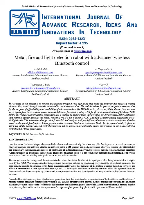
ISSN: 2454-132XImpact factor: 4.295(Volume 4, Issue 2)Available online at: Metal, fire and light detection robot with advanced wirelessBluetooth controlAkhil BaddiKoneru Lakshmaiah Education Foundation, Guntur,Andhra PradeshU NagamalleshKoneru Lakshmaiah Education Foundation, Guntur,Andhra PradeshPrashanth G RajuKoneru Lakshmaiah Education Foundation, Guntur,Andhra PradeshNiloy ChKoneru Lakshmaiah Education Foundation, Guntur,Andhra PradeshABSTRACTThe concept of our project is to control and monitor trough mobile app using blue-tooth the elements like based on sensing elements fire, metal through the code embedded in the microcontroller. The code is written in general purpose microcontroller for the purpose of affordability and availability of microcontrollers like MCS-51 series, pic-series, Motorola etc. Here we have taken inputs from three sensors named as a metal detector for metal sensing, LDR for fire and a combination of LDR and LED. All the above three convert analog parameters into a voltage by keeping them into potential divider networks. After calibration with potential divider network, the output voltage is fed to 8-bit, 8-channel ADC. The ADC converts analog parameters into 8-bit digital code. The microcontroller gets data from ADC and analyses with pre-defined values and takes necessary control action based on the pre-defined values. It has got two modes - Manual Mode and Automatic Mode. In the manual mode, it gives an alarm for all the parameters, but control action will not be taken. In the automatic mode, the program in the microcontroller controls all the three parameters.Keywords: Metal, Fire and Light Detection.1. INTRODUCTIONOn this mother Earth anything can be controlled and operated automatically, but there are still a few important sectors in our control where automation has not been adopted or not been put to a 100 percent use, perhaps because of several reasons like affordability and availability. Automation is a process of controlling of industrial machinery and processes, thereby replacing human operators. Although this set-up overcomes the problems caused due to human errors it is not completely automated and expensive. The system comprises of sensors, Analog to Digital Converter and Microcontroller.The sensors sense the change and the microcontroller reads this from the data at its input ports after being converted to a digital form by the ADC. The microcontroller then performs the needed actions by employing relays until the strayed-out parameter has been brought back to its optimum level. Since a microcontroller is used as the heart of the system, it makes the set-up low-cost and effective nevertheless. As the system also employs an LCD display for continuously alerting the user. Thus, this system eliminates the drawbacks of the existing set-ups mentioned in the previous section and is designed as an easy to maintain flexible and low-cost solution.An embedded system is a system which does a predefined task that is defined as a combination of both software and hardware. A general-purpose definition of embedded systems is that they are devices used to control, monitor or assist the operation of equipment, machinery or plant. "Embedded" reflects the fact that they are an integral part of the system. At the other extreme, a general-purpose computer may be used to control the operation of a large complex processing plant, and its presence will be essential.All embedded systems are including computers or microprocessors. Some of these mini computers are however very simple systems as compared with a personal computer. The very simplest embedded systems are capable of performing only a single function or set of functions to meet a single useful purpose. In more complex systems an application program that enables the embedded system to be used for a particular purpose in a specific application determines the functioning of the embedded system.The ability to have programs means that the same embedded system can be used for a variety of different purposes. In some cases, a microprocessor may be designed in such a way that application software for a particular purpose can be added to the basic software in a second process, after which it is not possible to make further changes. The applications software on such processors is sometimes referred to as firmware.The simplest devices consist of a single microprocessor (often called a "chip”), which may itself b e packaged with other chips in a hybrid system or Application Specific Integrated Circuit (ASIC). Its input comes from a detector or sensor and its output goes to a switch or activator which (for example) may start or stop the operation of a machine or, by operating a valve, may control the flow of fuel to an engine. As the embedded system is the combination of both software and hardware.Block Diagram Explanation:The block diagram shows the construction of the protection from the fire, smoke, and heat. The sensing of the three parameters by using the sensors these sensors send the analog information about the three parameters.The analog data is connected to the ADC controller. The ADC controller will convert the input analog data to the equivalent digital data. This data is given to the micro controller. Because of the micro controller can only understand the digital information only. The micro controller taka the data and store that data in the memory. This data is compared with the internal ideal data. If any change in the input data then the micro controller related change of the output device with respect to the change of the input device.The reset logic is used to protect the data stored in the micro controller when in the power spikes are present in the line voltage. From the circuit 5v, dc and 12 v dc is required to drive the all the components. The mains give the 230v ac so first we step down the 230v ac into 12v ac by using a step down transformer. Then the output is given to the full wave rectifier as given in the circuit diagram. The rectifier is eliminating the negative peek voltage of the input voltage the output of the rectifier is the pulsating dc as shown in the block diagram of the rectifier. The error pulses are eliminating using capacitor filter. Then the output at the parallel of the capacitor is the 12v dc. But the Micro Controller is work on 5v dc so convert the 12v dc in the 5v dc by using a regulator (7805) the output of the regulator is constant irrespective of the input voltage.The Micro Controller requires the preset logic circuit for protection of the internal program and internal clock when in the power failure. A sudden change in the power may cause data error. These types of the errors will corrupt the internal program. The reset logic circuit contains one capacitor and a resistor. This arrangement is shown in the Micro Controller circuit.RESET LOGICXTAL1 and XTAL2 are the input and output, respectively. An inverting amplifier which is configured an on-chip oscillator, as shown in Figure 1. Either a quartz crystal or ceramic resonator may be used. To drive the device from an external clock source, XTAL2 should be left unconnected while XTAL1 is driven as shown in Figure 2. There are no requirements on the duty cycle of the external clock signal since the input to the internal clocking circuitry is through a divide-by-two flip-flop, but minimum and maximum voltage high and low time specifications must be observed.Blue Tooth DataBluetooth is a radio standard and communications protocol primarily designed for low power consumption, with a short range (power-class-dependent: 1 meter, 10 meters, 100 meters) based on low-cost transceiver microchips in each device.Bluetooth lets these devices communicate with each other when they are in range. The devices use a radio communications system, so they do not have to be in the line of sight of each other, and can even be in other rooms, as long as the received transmission is powerful enough.Class Maximum Permitted Power(mW/dBm)Range (approximate)Class 1 100 mW (20 dBm) ~100 metersClass 2 2.5 mW (4 dBm) ~10 metersClass 3 1 mW (0 dBm) ~1 meterBluetooth is implemented in a variety of new products such as phones, printers, modems, and headsets. Bluetooth is acceptable for situations when two or more devices are in proximity to each other and don't require high bandwidth. Bluetooth is most commonly used with phones and hand-held computing devices, either using a Bluetooth headset or transferring files from phones/PDAs to computers.Bluetooth also simplifies the discovery and setup of services. Bluetooth devices advertise all services they provide. This makes the utility of the service that much more accessible, without the need to worry about network addresses, permissions and all the other considerations that go with typical networks.2. SOFTWARE USED∙Assembly language for 8052∙8052 Cross-compiler∙Universal Programmer soft ware∙ORCAD for PCB designing and layout.3. ADVANTAGES∙Small in size∙Easy to controlling the heat, smoke, and fire.∙Cost of manufacturing is moderate.4. DISADVANTAGES∙Complete automation in terms of pest and insect detection and eradication cannot be achieved.∙No self-test system to detect a malfunction of sensors.5. APPLICATIONS∙Used in industries.∙Used in military applications∙Used in power stations.∙Used at boilers.6. RESULTAUTOMATICAL DETECTOR the three parameters fire, METAL, heat are detected and controlled. The fire was detected by the LDR and can be observed in the LCD provided and controlled automatically through the wmotor to the motor driver. Similarly, a combination of LDR and LED detects the smoke when it exceeds a certain limit. When this occurs, the buzzer will start automatically and the amount of smoke that is detected is displayed in the LCD. Metal is detected with the metal detection sensor and as the metal is detected there is an alarm7. CONCLUSIONIf the project is to control and monitor trough mobile app using blue-tooth the elements like based on sensing elements fire, heat through the code embedded in the microcontroller. We have written a code in general purpose microcontroller for the purpose of economy and availability of microcontrollers like MCS-51 series, pic-series, Motorola etc. Here we have taken inputs from three sensors named as thermostats for temperature, LDR for fire and a combination of LDR and LED. All the above three convert analog parameters into a voltage by keeping them into potential divider networks. After calibration with potential divider network, the output voltage is fed to 8-bit, 8-channel ADC. The ADC converts analog parameters into 8-bit digital code. The microcontroller gets data from ADC and analyses with pre-defined values and takes necessary control action based on the pre-defined values. It has got two modes - Manual Mode and Automatic Mode. In the manual mode, it gives an alarm for all the parameters, but control action will not be taken. In the automatic mode, the program in the microcontroller controls all the three parameters.8. REFERENCES[1] Muhammad Ali Mazidi, Janice Gillispie Mazidi, Rolin D. Mc Kinlay , nd The 8051 Microcontroller & Embedded Systems, Pearson Education Inc. 2 Edition, 2008.[2] Myke Predko, Programming and Customising the 8051 Microcontroller, TMH, 1999.[3] Kenneth J Ayala, the 8051 Microcontroller Architecture, Programming & Applications Penram International, 2nd Edition, 1996.。
6 Steps to Fielding Smart, Integrated C4ISR SystemsL3Harris TechnologiesTHIS INFORMATION IS NOT EXPORT CONTROLLED THIS INFORMATIONIS APPROVED FOR RELEASE WITHOUT EXPORT RESTRICTIONS INACCORDANCE WITH A REVIEW OF THE INTERNATIONAL TRAFFIC INTABLE OF CONTENTS Executive summary (3)Start with your end goal in mind (4)Design for ease-of-use and rapid deployment (5)Beware of introducing information overload (6)Build on your existing systems as you add new capabilities (7)Plan for post-acquisition training, support and maintenance (8)Demand a focus on sovereignty (9)6 Steps to Fielding Smart, Integrated C4ISR Systems EXECUTIVE SUMMARYPutting the necessary assets and infrastructure in place to create a real-time, multi-echelon Common Operational Picture (COP) is the desire of most militaries. But fielding these smart, integrated, cognitive systems can become overly complicated, costly and time-consuming—hindering their effective implementation in the short term and over time.Your ability to overcome the complexities, timelines and cost challenges associated with C4ISR system integration—and to ensure the integration is sustainable over time—is closely tied to the partner you choose to work with. Having a partner that serves as a trusted advisor with the experience and willingness to put your needs first (selling capability instead of products) is a critical success factor.L3Harris is the established leader in developing and deploying customized, integratedC4ISR systems and the infrastructure needed to gather, synthesize and share a diverse range of battlefield reconnaissance data. Our long history of being there “in field” with our customers through times of peace and conflict positions us to recommend solutions that help the world’s militaries put intelligence into action. Success can be fast-tracked, deploying pre-configured packages available for quick delivery as building blocks to an otherwise complex, bespoke system implementation.Here are the top 6 pre-purchase steps that should be considered when developing and implementing an integrated C4ISR system:1. Start with your end goal in mind2. Design for ease-of-use and rapid deployment3. Beware of introducing information overload4. Build on your existing systems as you add new capabilities5. Plan for post-acquisition training, support and maintenance6. Demand a focus on sovereignty1. Start with your end goal in mindOUR OBSERVATION: Choose a partner with direct access to the necessary technologies and proven experience in developing and deploying integrated military command systems. The best partner will understand and anticipate the specific needs of each user group from headquarters to the front line. Ensure your partner can demonstrate their understanding of how users will be impacted by the result, as well as the journey during implementation. That partner should play an advisory role throughout the process, helping you to:•Understand how you are operating today likely differs from what you will be doing tomorrow. It’s not enough to simply update systems. Commanders must understand and articulate the benefits of increased C4ISR awareness well before delivery so that new doctrine can be written, and end users can be trained prior to fielding. Following this type of implementation strategy will greatly reduce the time it takes to get from delivery to improved, real-time tactical decision making.•U se focused terms for what you’re trying to achiev e. It may not need to be a nationwide C4- or C5ISR system. The scale and scope of your migration should be based on your actual needs today—and not become overcomplicated by extra capabilities you may not use.•Develop specific, measurable goals and objectives for each stage of the project. The overall objective is to get the right information to the right personat the right time to enhance decision making. Plan a number of steps in yourdevelopment. New capabilities, delivered incrementally, allow for short-termsuccesses in pursuit of the greater goal.•Count on your partner to develop a vision that delivers on your specific measurable goals and objectives. You are purchasing experience, labor and services as much as technologies and equipment. Your partner should show how they plan to help you ensure forward and backward interoperability and avoid“analysis paralysis” by solving today’s mission while leaving room for futuregrowth and adaptation.L3Harris is ideally suited to guide you on your journey, given our decadesof experience in the international systems market, demonstrated customer relationships, in-country partnerships (175+) and reputation as cutting-edge integrators. This combination of reputation and knowledge drives us to have the right conversations with the right people—and to solve today’s mission challenges while planning for the requirements for future adaptation. Along with our position as a world leader in waveform development and fielding, we bring valuable real-life experiences to the implementation of C4 Battle Management Systems (BMS) and related solutions.2. Design for ease-of-use and rapid deploymentOUR OBSERVATION: Systems must be designed with your current end user’s capabilities in mind. The easier a system is to use, and the faster it can be deployed, the more likely it is to be adopted and implemented to its full potential. Highly effective system designs:•Understand that a soldier’s user experience is key to both the adoption and effectiveness of a given solution. The goal is to free up users so they can spend more time on valuable situational analysis and less on figuring out how to use agiven system.•Take an iterative approach. Start with what you have (tactical radios, for example) and build from there so new capabilities can be fielded quickly and more easily.Teach users how to adopt new technologies in iterative content blocks to avoidoverwhelming them all at once.•Include a cadence of new capability “quick wins.” Incremental successes will demonstrate a measurable return on investment to stakeholders up and down the command chain. They will also help to keep your users engaged in the development, design and delivery process, while building consensus regarding next stepsduring fielding.•Stay focused on the need. Since new program phases are often budget-driven, put your resources into what is most critical for sovereign protection, rather thanadditional advanced features you may not be ready for, or able to implement totheir full potential.L3Harris takes the user experience seriously, and our 50 years in the field—combined with a workforce comprising 15% ex-military personnel—havehoned our understanding of how technologies are used in the real worldunder high-stress conditions. This extends even to small details, like how easyit is to operate a radio while wearing gloves, or how a piece of technology with extraneous light or sounds could inadvertently reveal locations at night.3. Beware of introducing information overloadOUR OBSERVATION: Relying on an ever-increasing number of battlefield sensors presents a significant challenge: how to process all the data collected by each sensor and deliver relevant situational understanding in real time to aid in decision making. Collecting the information from tens to hundreds of sensors in the field creates more information than the human mind can interpret; therefore, an effective system must provide some information processing and simplification:•Identify who needs what data, when. It will no longer be possible for everyone to know everything. Data will be delivered at different need and classification levels so that various decision makers will only receive what they need, when they need it. •Understand that Artificial Intelligence (AI) is not just hype, it is a requirement.Data collection, analysis and target identification need to be implemented in-fieldtoday. As your partner, we will help identify what data should be processed where, how it can be automated, when human input is necessary or desired, and whereto use each tool. For example, a warfighter engaged in combat often can’t readdetailed environmental information in real time. By presenting the data graphically using visualization tools, the same information becomes instantly actionable in atime-critical decision-making process.•To design for project success, start small and build gradually.Don’t change or replace everything at once. It’s better to make incremental changes to data collection and processing that will help users adapt and adopt more easily.L3Harris will implement systems that deliver relevant information to each operational role using machine learning and AI to control information overload and keep warfighters laser-focused on their tasks.4. Build on your existing systems as youadd new capabilitiesOUR OBSERVATION: Many vendors are more proprietary than they admit. Inevitably, lack of interoperability (or imperfect interoperability) can result in missed data—and even missed targets. True interoperability requires proactive effort on the part of the integrator. Although the industry claims to operate on an “open systems” architecture, the reality is that many aren’t there yet. Proactive, effective integrators will continually:•Invest in developing two-way, responsive relationships. Look for a partner witha record of industry collaboration and th e ability to leverage relationships to get whatthey need from other suppliers.•Take your own buying habits into account. Many purchasers buy for a specific mission, program, or end user, resulting in splintered acquisitions over time. Consider an evolving procurement approach with a focus on long-term program sustainability rather than a “big bang” single-need or one-off purchase.•Develop a phased plan that ensures each program investment solves both immediate problems and longer-term goals. Don’t sacrifice the future for a“right now” solution.•Steer away from partners who force a single-system approach, and who will hold you hostage to their products for future interoperability. You need to be able to plug new capabilities into your C4ISR solution—and they won’t necessarily come from the same vendor. Stressing the use of open standards eases this problem. L3Harris is relentlessly focused on open architecture and open systems.Our industry relationships and integration experience, along with our commitment to understanding and solving the specific challenges faced by our customers, translateto robust solutions and the ability to deliver advanced capabilities today without limiting the possibilities for tomorrow.5. Plan for post-acquisition training, support,and maintenanceOUR OBSERVATION: Purchasers often don’t consider the ongoing trainingand maintenance requirements—and costs—for the systems they buy. It’sup to us to be your partner and help ensure you plan accordingly and to the appropriate budget levels:• A system that lacks proper training/maintenance funding will not be used or usable. Plan for up to 15%–20% ongoing costs above and beyond the initial system investment.•Understand the emerging battlefield environment and develop new concepts of operation, as well as determine how these approaches will impactperformance. In a sense, your partner will need to understand the big picture as well as or better than you do, given duty rotations and other operationalrealities. They should provide a level of continuity to help maintain their corporate knowledge—and your institutional knowledge—as personnel come and go.L3Harris is known for industry-leading post-delivery support and sustainment packages tailored to specific customer needs. We offer a wide range of services, such as installation, maintenance support, sovereign maintenance capability, training, and in-field customer support. Every system, whether turnkey or custom-built, is delivered with detailed user documentation as well as maintenance schedules.6. Demand a focus on sovereigntyOUR OBSERVATION: This is only possible when a partner has an absolute commitment to their customers’ sovereignty—and is willing to make investments to support and develop local workforces in every region in which they operate. Having a sovereign-focused mindset will ensure you can:•Work with your partner to source labor and materials locally. For example, rather than ship shelters from an out-of-country vendor, find the shelters locally, fit them out locally, and you’ll be creating a trained workforce rather than simply importing finished products.•Plan for local delivery of training, service and maintenance over a period of time. This will help to create local jobs and build the local economy.•Identify a partner that uses local relationships that can be leveraged throughout the planning and implementation process, including thedevelopment of specific technologies that can further local capabilities.L3Harris is committed to local partnering and has a long history of partnershipin the countries we serve. This is a core element of our business process atL3Harris, and one of the reasons we are able to achieve such close customer relationships. For example, in Australia, L3Harris has created opportunitiesfor over 500 full-time local employees and fostered ongoing technology innovation. Formoreinformation,contactJakeWilliams(**************************).。

综合英语4-第三单元unit3课文1 The term "organic architecture" was coined by Frank Lloyd Wright(1867 - 1959).It is a philosophy of architecture that promotes harmony between human habitation and the natural world through design approaches,which are so sympathetic and well integrated with its site that buildings,' furnishings, and surroundings become part of a unified, interrelated composition According to Wright, the idea of organic architecture refers not only to the buildings' literal relationship to the natural surroundings,but also how the buildings' design is carefully thought out as a unified organism Geometries throughout Wright's works build a central mood and theme. Essentially organic architecture is the literal design of every element of a building: from the windows, to the floors, to the individual chairs, intended to fill the space. Everything relates to one another, reflecting the symbiotic ordering of systems of nature.2 Organic buildings are characterized by wavy line, and curved shapes that suggest natural forms, instead .of being linear or rigidly geometric. Wright once said that all twentieth century, Modernist architects took the concept of organic architecture to new heights. By using new forms of concrete and cantilever trusses,architects could create swooping arches without visible beams or pillars.1“有机建筑”一词是由弗兰克·劳埃德·赖特(1867-1959年)创造的)。
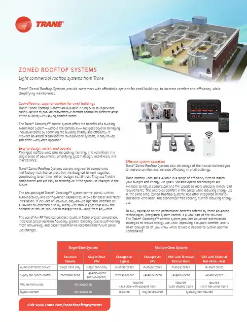
visit /zonedrooftopsystemsEf fi cient system operationTrane® Zoned Rooftop Systems take advantage of the newest technologies to improve comfort and increase ef fi ciency in small buildings.Trane rooftop units are available in a range of ef fi ciency tiers to match your budget and energy use goals. Variable-speed technologies areavailable to adjust compressor and fan speeds to more precisely match load requirements. This improves comfort in the space while reducing energy use at the same time. Zoned Rooftop Systems also offer integrated demand-controlled ventilation and economizer free cooling, further reducing energy use.To fully capitalize on the performance bene fi ts offered by these advanced technologies, integrated system control is a vital part of the solution. The Tracer® Concierge™ control system provides advanced optimization strategies to reduce energy use while improving occupant comfort, and is smart enough to let you know when service is needed to sustain optimal performance.Cost-effective, superior comfort for small buildingsTrane® Zoned Rooftop Systems are available in single- or multiple-zone con fi gurations to provide cost-effective comfort control for different areas of the building with varying comfort needs.The Tracer® Concierge™ control system offers the bene fi ts of a building automation system—without the complexity—and goes beyond managing individual rooms by operating the building smartly and ef fi ciently. It provides advanced capabilities for multiple-zone systems, is easy to use, and offers worry-free operation.Easy to design, install, and operatePackaged rooftop units provide cooling, heating, and ventilation in a single piece of equipment, simplifying system design, installation, and maintenance.Trane® Zoned Rooftop Systems use pre-engineered components and factory-installed controls that are designed to work together, contributing to on-time and on-budget installation. They use familiar components and are easy to recon fi gure if the space use changes in the future.The pre-packaged Tracer® Concierge™ system control panel, with its auto-discovery and con fi guration capabilities, allows for easier and faster installation. It includes an intuitive, easy-to-use operator interface on a 10-inch touchscreen display, along with mobile apps that allow the operator or service provider to manage the building from anywhere.The use of Air-Fi® Wireless controls results in faster project completion, increased sensor location fl exibility, greater reliability due to self-healing mesh networking, and easier relocation to accommodate future space use changes.ZO N E D R O O F TO P S YS T E M SLight commercial rooftop systems from TraneTrane® Zoned Rooftop Systems provide customers with affordable options for small buildings, to increase comfort and ef fi ciency, whilesimplifying maintenance.VAV terminal units (200 to 8000 cfm)• Trane fl ow ring provides unmatched air fl ow measurement accuracy and control • Durable, heavy-gauge air valve cylinder• modulating control• Air-Fi® Wireless communications • Retro fit dampers available for upgrading existing systemsTrane - by Trane Tech nologies (NYSE: TT), a global climate innovator - creates comfortable, energy efficient indoor environments for commercial and residential applications. For more information, please visit or .Trane h as a policy of continuous product and product data improvement and reserves th e righ t to ch ange design and specifications without notice. We are committed to using environmentally conscious print practices.All trademarks referenced are the trademarks of their respective owners.©2020 Trane. All Rights Reserved. ENV-SLB024C-ENNovember 5, 2020•single piece of equipment• able-speed fan control• Three tiers of effi ciency: standard, high, or ultra-high•••Pre-programmed, factory-installed ReliaT el™ DDC controls with wired or Air-Fi® Wireless communicationsAir-Fi® Wireless controls• Eliminates wires between equipment controllers and zone sensors, and between equipment and system controllers, allowing for faster installation, increased location fl exibility, and easier relocation• Self-healing wireless mesh and extended signal range maximize reliability• Supports open communication protocols through conformance with ASHRAE® Standard 135 (BACnet®/ZigBee®)• Up to four sensing functions in one zone sensor: temperature, humidity, occupan-cy, and CO 2• 15-year lifetime batteries。
INNOVATIVE PV MICRO-INVERTER TOPOLOGY ELIMINATES ELECTROLYTIC CAPACITORS FOR LONGER LIFETIMEWard Bower1, Rick West2, Art Dickerson31Sandia National Laboratories, Albuquerque, NM 87185; USA, wibower@ 2Distributed Power, San Luis Obispo, CA 93401; USA, Rick.West@ 3Bluepoint Associates, San Luis Obispo, CA 93401; USA, adickersn@ABSTRACTAn extremely reliable micro-inverter is critical to the success of the AC PV Building Block and the AC PV Module concepts.[1,2,3,4]An innovative inverter design has been developed and prototyped in order to address some of the most critical issues associated with extending the mean time between failure (MTBF) and the total lifetime of the micro-inverter when it is integrated onto a PV module. The innovative micro-inverter addressed in this paper uses a unique proprietary circuit topology to reduce the numbers and sizes of capacitors, is currently rated at 150W, and has been shown to be thermally robust and feasible. Additionally, the smaller capacitors used in the design use advanced technology exhibiting much longer lifetime (30-year)in the anticipated thermal environment. The unconventional micro-inverter design considerations, layout, early findings from modeling and evaluation results are presented.Preliminary findings for a proposed redesign to increase the rating to 300W are presented.An initial assessment of a reliability requirement study for micro-inverters is also discussed.[5]INTRODUCTIONThe concepts known as the AC Photovoltaic Building Block and AC PV module can revolutionize the photovoltaic industry by offering ultimate plug-n-play products that need no system designer and that can be sold directly to the customer as a complete system.[4] Both concepts offer sweeping technical and installation challenges as well as advantages over the conventional photovoltaic system. With the AC PV Building Block, photovoltaic modules are fully integrated with a micro-inverter mounted into the frames or rails. The frames and rails also serve as approved electrical conduit, micro-inverter housing, enclosed interconnects, ac buses,and safety device housings. They could be marketed as a complete,certified plug-and-play system.The AC PV Building Block concept can easily reduce other balance-of-systems (BOS) and installation costs by at least 50% and can improve reliability through mass production and ease of installation by offering a standardized, snap-together, modular design. The success of implementing both concepts relies on: (1) mass-production of extremely high quality components using the latest technology and (2) all of the elements and components integrated together into a rugged, reliable, low cost, and proven package. The integrated micro-inverters must have lifetimes and mean time between failures (MTBF) comparable to the 20-30 years common in today’s high quality silicon photovoltaic modules.The fully-packaged nature of the AC PV Building Block concept brings utility-compatible photovoltaic products directly to the utility-interactive market by eliminating many design, installation, and purchasing headaches. The concept can also be used in hybrid and stand-alone applications with little or no change to the micro-inverter or internal package, but with small additional control schemes for the system.The topology, design and construction of a micro-inverter that is to be mounted upon or near to PV modules cannot be business as usual. One objective of this project was to prove the feasibility of a new innovative inverter design that uses no electrolytic capacitors. A second wasto show that the inverter operates in a package layout consistent with being contained within the frame of a PV module or as a rail member that is also used for mounting the PV module. Lifetime and MTBF issues for micro-inverters are predominantly electrolytic capacitors and thermal management because they are exposed to brutal environmental conditions that are not commonly addressed for typical consumer electronic circuitry. Other critical reliability-sensitive considerations included surge protection (on the ac and dc side), long-lived connectors, corrosion resistant interconnects, and improved magnetic materials. A commercially available wide-band-gap semiconductor device was included in this design,but as more advanced wide-band-gap devices become economically available it is expected even more lifetime issues will be eliminated.Employing the evolutionary technical innovations of devices and components in new micro-inverter designs can incrementally improve the lifetime of micro-inverters, but the environment presented on rooftops and the close coupling with photovoltaic modules virtually dictates a need for leapfrog advances in some components and micro-inverter designs. Innovative circuitry can revolutionize inverter designs by eliminating short-lived components and utilizing digital signal processing coupledto state-of-the-art integrated devices. This prototype development was a first step, and was intended primarilyto prove the feasibility of the innovative circuitry and to study the thermal management aspects of the unique packaging layout that fits into a frame (bar in Fig. 1) or railof a PV module.The initial success has prompted a newprototype design to operate at a 300W level as discussed later in this paper.As already indicated,the innovative micro-inverter described in this paper uses a unique circuit topology to reduce the numbers and sizes of capacitors. Additionally, the smaller capacitors used in the design use an advanced technology exhibiting much longer lifetime (30-year) in the expected environment. The innovative circuit uses the advantages of a single photovoltaic module package, close dc coupling that reduces inductive issues, simplified controls for maximum-power-point-tracking and dc set points, high-speed switching, no system diodes and other cost saving plug-and-play AC PV Building Block features as shown in Fig.1.[4]The PV module chosen for this prototype was a 72-cell, BP Solar,multi-crystalline technology.It has a nominal maximum power point (MPP) at 30 to 34 Vdc and a (STP)power rating of 160W.This prototype micro-inverter required a boost circuit with a significant voltage boost ratio ranging from 10 to 14 with this PV module. This high boost ratio resulted in inverter losses that can easily be reduced with higher maximum power point voltages.The likelihood of PV manufacturers marketing higher voltage modules in the 150-W power ranges rests entirely upon prospects for a very large market for the AC PV Building Block or AC PV modules. The real trade off that must be considered is whether a more complex PV module with more series tabs or a micro-inverter with higher efficiency fits into the design for the desired end product.[6,7]Advanced power semiconductors, including some silicon-carbide devices are becoming commercially available at reasonable costs and are being included in the new design.[7]An ultimate goal is to use additional high-temperature wide-band-gap devices in future iterations. Higher temperature operation with improved lifetimes and high-speed performance are some advantages offered by newly-developed silicon-carbide power switches and diodes,but it must be noted that with higher temperatures, the entire package must be innovative to prevent detrimental thermal effects on other conventional electronic components.INVERTER COSTSCosts remain a critical issue for successful AC PV Building Block micro-inverter designs. The cost of a complete AC PV Building Block or AC PV module can generally exceed the cost of a conventional PV system because lower installation costs, modularity, flexibility in orientation, array utilization and overall performance will likely otherwise lower installation costs. The additional cost of the micro-inverter for the AC PV Building Block must be a consideration of final designs, but must be balanced with performance and high reliability.[6] Today’s cost goal for the complete integrated product in quantities of greater than 10,000 is a cost of less than $4.50/W. That is slightly higher,but consistent with the new U.S.Department of Energy Solar America Initiative goals that are targeting levelized cost of energy (LCOE) for PV power generation of $.08 to $.10/kWh by the year 2015for residential size systems.[8]The higher AC PV Building Block cost must be balanced with value added features that include built-in communications either via power-line carrier or wireless, and plug-n-play features that reduce installation expenses.F eatures including advanced integrated surge suppression, input and output communications with the consumer, advanced digital signal processing, and electromagnetic susceptibility must be designed into the final micro-inverter. Cost and surge issues were priority considerations in the developed prototype and that work is continuing. Table 1 shows estimated costs and the (elongated)form factor for various power ratings of the innovative inverter.Table 1. Estimated costs and thermal considerations for the innovative micro-inverter designINVERTER PERFORMANCEThis innovative micro-inverter design,suitable for use with AC PV modules or the AC PV Building Block concept has been completed and preliminary evaluations are now complete. As noted, the prototype design addressed only the most critical issues associated with extending the mean time between failure and the total lifetime of a micro-Fig. 1. Artists Concept of an AC PV Building Blockinverter for an AC PV Building Block. Both frame and rail applications are being considered with plans to use the same micro-inverter design and layout in each. Results from circuit modeling, simulations and bench testing are very encouraging.Array utilization has been simulated using input from measured parameters and found to be nearly 100%, even with fast moving clouds. Other simulations and bench testing have aided in selecting components, compensation factors, and determining some of the effects of different switching frequencies.The measured efficiency is consistent with design calculations,but must be improved for the final design. Conducted and radiated electromagnetic susceptibility and emanations have been measured and were not problematic,and in fact, additional filtering on the ac line was not needed. Surge protection remains unmeasured at this time and studies are ongoing. The evaluation results have been very encouraging prompting further evolution of the design to a 300-W rating. Slightly more than a 300-W rating will be necessary to accommodate the largest PV modules that are available today.A State Energy Program(SEP) Special Projects program conducted by the U.S.Department of Energy has issued a grant to measure, model and analyze the operating environment experienced by the micro-inverter mounted on the back of the 300-W PV module.[5]To accomplish this,several non-functional prototypes will be constructed and installed at several test facilities where instrumentation will fully characterize temperatures and other parameters over an extended period if time. Several different inverter attachment methods will be investigatedto ascertain the impacts on thermal operating conditions. These investigations will lay the groundwork for more extensive thermal modeling, innovative thermal management, electronic circuit design analysis and lifetime assessment for the micro-inverters now in development.Figure 2shows the prototype constructed for thermal analysis reported herein. Preliminary measurements indicate that a heat sink will not be needed for 150-W ratings. Initial validation of the circuit topology has shown impressive performance with only a few areas needingimprovements. F igure 3 shows a close-up showing theinput capacitor for this prototype. The resulting dc current ripple,that is generally significant with single-phase inverters,is shown in Fig.4with a reference to half sine current. The dc current ripple is only 0.3%when the power delivered is 90W in this oscillograph. This low value of dc ripple allows excellent array utilization and maximum-power-point tracking. F igure 5shows the output power and the array voltage ripple. The ripple represented here is accomplished with the3.3 µF filtercapacitor at the PV module (dc)input of the inverter.The peak efficiency of this prototype was measured to be in the high 80s. This relatively low peak efficiency is primarily a result of off-the-shelf magnetic components that were used for the proof-of-feasibility prototype,and to a lesser extent that discrete control components are currently being used instead of a digital signal processor with integrated controls.It is estimated that core magnetic losses can be reduced by 50%with advanced magnetic materials. Further, since this unit was constructed,new semiconductor devices have been announced with Fig. 3. Micro-inverter input section showing the small3.3 µF filter capacitor.Fig. 2.Micro-inverter prototype layout for the thermal analysis project Half-PM3394A DC Currentadvanced MOSFET switches exhibiting a 50% reduction in on-resistance.Additionally, the use of a digital-signal-processor(DSP),an optimized switching frequency and integrated controls will further improve efficiency and reduce internal heat generation.It has been estimated through calculations and analysis that advanced magnetic core materials and lower on-resistance MOSF ETs alone will permit operation of this prototype with 300-W PV modules having a maximum-power-point rating around92V. This improved power rating is related to the fact that over 50% of the losses in the prototype derive from I2R sources, while approximately 20% derive from other sources that vary with power throughput. Thus a 300-W unit compared to the 150-W unit would have a reduction in I2R losses approximately equal to the proposed increase in power-throughput losses. In essence, the heat release of the lower current 300-W unit would essentially equal that of the higher current 150-W unit.Computer simulations using SPICE also have been run for PV modules of 200W at 40V and 300W at92V MPP ratings. The simulations verify the early calculations cited above. The SPICE simulations also agree closely with the still-air tests at ambient air temperatures up to 60°C which were conducted on the original feasibility prototype.CONCLUSIONSThe innovative inverter topology, the circuit layout and the design concept have been shown to be feasible and the very encouraging results have been nearly as originally calculated. Cost estimates are consistent with the needs for the AC PV Building Block or AC PV modules and with the goals of the U.S. Department of Energy Solar America Initiative. Initial thermal analysis shows the design resulted in adequate thermal dissipation when the 150-W inverter is mounted within a frame of a PV module.F urther thermal analysis and performance studies are being conducted as part of a U.S. Department of Energy, State Energy Program Special Projects study to determine the extremes and ranges of environmental requirements expected for micro-inverters. The study is now under way.A redesigned, higher voltage, higher power throughput micro-inverter with ratings up to 300W is being designedusing the same control package and with advanced andhigher voltage power handling components.ACKNOWLEDGEMENTSSandia is a multiprogram laboratory operated by Sandia Corporation, a Lockheed Martin company, for the U.S.DOE National Nuclear Security Administration under contract DE-AC04-94AL85000. The authors wish tothank Dr. Jean Posbic of BP Solar for providing the PV modules used in this development.REFERENCES[1]Kern, G., “SunSine™300: Manufacture of an AC Photovoltaic Module,” A PVMaT Contractors Final Reportby Ascension Technology, Phases I & II, NREL/SR-520-26085, Golden, CO, Mar 1999.[2]Odenkamp, H., deJong I., Baltus, C., Verhoeven, S., Elstgeest, S., "Reliability and Accelerated Life Tests of theAC Module-mounted OKE4 Inverter," Proceedings of the25th IEEE Photovoltaic Specialists Conference, Washington, DC, May 13-17, 1996.[3]Strong, S., Wohlgemuth, J., Kaelin, M., Development Standardized Low-cost AC PV Systems: Phase I Annual Report, A PVMaT report by Solar Design Associates, Solarex and Advanced Energy Systems, NREL/SR-520-23002, Golden, CO, Jun 1997.[4]Bower, W., The AC PV Building Block -Ultimate Plug-n-Play That Brings Photovoltaics Directly to the Customer, Proceedings of the 2004 PV Program Review, Denver,CO, Oct 24-27, 2004.[5]“Evaluation and Analysis of the Thermal Environmentfor a Module-Integrated Micro-Inverter”, State Energy Program (SEP) Special Projects, Project DE-PS26-05NT42396-07.[6]Ton, D., Bulawka, A., Bower, W., Summary Report onthe DOE Workshop On a Systems-driven Approach To Inverter Research and Development, U.S.Department of Energy,EERE Solar Technology Program, /solar/pdfs/sda_inverter.pdfSep 2003.[7] Ton, D., Bower, W., Summary Report on the DOEHigh-tech Inverter Workshop; U.S. Department of Energy,EERE Solar Technology Program, /solar/pdfs/inverter_II_workshop.pdf; Jan 2005.[8]“Notice of Program Interest: DE-PS36-06GO96020,”U.S.Department of Energy, Solar Technologies Program,/solar/about.html, Mar 2006.Fig.5. Power output (60W/div) and PV module voltage (1V/div “ac”coupled)。
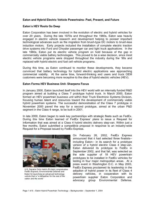
Eaton and Hybrid Electric Vehicle Powertrains- Past, Present, and FutureEaton’s HEV Roots Go DeepEaton Corporation has been involved in the evolution of electric and hybrid vehicles for over 20 years. During the late 1970s and throughout the 1980s, Eaton was heavily engaged in electric vehicle research and development helping to pioneer important technological advances such as the migration from brush-type DC motors to brush-less induction motors. Early projects included the installation of complete electric traction drive systems into Ford and Chrysler passenger car and light truck applications. In the late 1980s, Eaton put its electric vehicle program on hold because of the gap in commercially viable battery technologies. This proved to be a wise decision, since most electric vehicle programs were dropped throughout the industry during the ‘90s and replaced with hybrid electric and fuel cell vehicle programs.During this time, as Eaton continued to monitor these developments, they became convinced that battery technology for hybrid electric applications was approaching commercial viability. At the same time, forward-thinking end users and truck OEM customers were becoming more receptive to the idea of hybrid electric vehicles (HEV).Eaton Forms HEV Business Unit- Sharpens FocusIn January 2000, Eaton launched itself into the HEV world with an internally funded R&D program aimed at building a Class 7 prototype hybrid truck. In March 2000, Eaton formed an HEV powertrain business unit within their Truck Electronic Systems Division, focusing human talent and resources toward the development of commercially viable hybrid powertrain systems. The successful demonstration of the Class 7 prototype in November 2000 paved the way for a second prototype, aimed at the urban P&D segment in the Class 4 range, to be built in 2001.In late 2000, Eaton began to seek key partnerships with strategic fleets such as FedEx. During this time Eaton learned of FedEx Express’ plans to issue a Request for Information that was aimed at a Class 4 hybrid electric delivery step-van. Within just a few months, Eaton submitted a competitive proposal in response to an industry-wide Request for a Proposal issued by FedEx Express.On February 26, 2002, FedEx Expressannounced that it had selected three finalists--including Eaton-- in its search for a prototypeversion of a hybrid electric Class 4 step-van.Eaton delivered its prototype to FedEx inSeptember 2002, and that fall, was selected asthe sole supplier of 18 HEV powertrainprototypes to be installed in FedEx vehicles fortesting in four major metropolitan areas. At apress event in Washington D.C. in May 2003,FedEx Express proclaimed its leadership in the adoption of hybrid power in its fleet of Class 4 delivery vehicles, in cooperation with its powertrain supplier Eaton Corporation and advocacy group Environmental Defense.U.S. Senator Orrin Hatch (R-Utah) congratulates FedEx Express, Environmental Defense andEaton for launching an advanced technology vehicle that is "a bellwether for the rest of the nation and the world."Adding importance to the event were appearances by U.S. Senator Orin Hatch (R-Utah) and Environmental Protection Agency director Christine Todd-Whitman, both hailing the announcement as a real and positive step towards the adoption of fuel-saving and pollution-reducing technologies.Meanwhile, in September 2002, Eaton was awarded a $7.1 million contract to lead a project in the Advanced Heavy Hybrid Propulsion System (AHHPS) Program sponsored by the U.S. Department of Energy. Through this program Eaton, in partnership with International Truck & Engine, will develop a heavy hybrid propulsion system designed to increase fuel efficiency and decrease emissions for commercial vehicles in the Class 4-7 weight range. Recently, a prototype UPS urban delivery vehicle was built using this new system and is currently in the testing stage.At the state capitol ceremony in SacramentoFedEx Express President David Bronczek explains the FedEx hybrid program to California Governor Arnold Schwarzenegger while Eaton’sJim Sweetnam and Fred Krupp of EnvironmentalDefense look on. On March 30, 2004, at a state capitol ceremonyin Sacramento, CA, FedEx Express, incollaboration with Sacramento Metropolitan AirQuality Management District and EnvironmentalDefense, placed the first of 18 Eaton hybridelectric powered delivery vehicles into service.The official rollout of the FedEx OptiFleet E700took place on the capitol steps with CaliforniaGovernor Arnold Schwarzenegger inattendance. Since late February, two FedExOptiFleet vehicles have been tested in theSacramento area to demonstrate thecommercial viability of the lower-emissionpowertrain in heavy-duty vehicles. Throughout the rest of 2004, Eaton will be placing an additional 16 trucks into service in selected cities. These trucks will endure real-world FedEx operating conditions to verify and provetheir viability in commercial applications.In May 2004, Eaton, in collaboration with International Truck and Engine, submitted a proposal to build a hybrid electric drive system for heavy-duty utility trucks. The proposal was submitted in response to a Request for Proposal from the HTUF Utility Hybrid Truck Working Group (Hybrid Task Force). Before submitting their proposal Eaton and International conducted several “Day-in-the-Life” sessions with members of the HTUF Utility Task Force Fleets. These sessions were held to better understand how the equipment is used in the field and have directly impacted the proposed design. In August 2004, the HTUF Working Group notified Eaton and International that their proposal had been selected.In October 2004, Eaton will host the fourth annual national meeting for the Hybrid Truck Users Forum (HTUF) in Kalamazoo, MI. In addition to hosting the event, Eaton will showcase several HEV commercial vehicle prototypes of varying vocations with a “ride-and-drive” at the Eaton Proving Grounds in Marshall, MI.Eaton’s Hybrid Mission & StrategyHybrid electric systems are critical to the automotive and truck industry’s technological roadmap that ultimately leads to fuel cell powertrains and beyond. The successful introduction of electric motor drives, inverters, energy storage devices and advanced power management controls on HEVs will pave the way for future migration to fuel cell powertrains.Eaton recognizes that in order to be commercially viable, hybrid electric vehicles will need to deliver significant fuel savings and environmental benefits. They are convinced that the most successful hybrid products will have the lowest price premiums compared to conventional vehicles as well as demonstrate exceptional reliability “out-of-the-box.” These objectives are what drives Eaton’s commitment to develop a hybrid electric system that will enable truck OEMs and engine manufacturers to comply with strict emissions regulations, reduce fuel consumption, improve drivability and increase functionality by providing on-board electrical power generation.By combining their successful automated manual transmission and clutch products with electric motor drives and related components, Eaton will be able to create integrated hybrid drivetrain units that are attractive to various commercial truck segments.Product Strategy: Series Vs. ParallelWhen building an HEV powertrain there are two basic configurations: series and parallel.• A “series” configuration has a generator mounted directly to the engine. All power from the engine is converted directly into electrical energy, which is then used to drive traction motors at the axle or wheel ends. In this type of design there is no mechanical drive path between the engine and the drive wheels.• A “parallel” configuration maintains conventional mechanical drivetrain architecture, but adds the ability to augment engine torque with electrical horsepower. A parallel system provides operating redundancy not found in a series system, whereby the conventional power can continue to operate in the event of an electrical power malfunction.Eaton is focused on developing parallel-hybrid drivetrainsystems that provide the best cost-benefit balance formany commercial truck applications. Most hybridsuppliers began working on series-hybrid systems andhave since transitioned to parallel hybrid architecture forsimilar reasons.Eaton’s first prototype truck featured a Full Hybridsystem that made it possible to operate the engineindependently from the vehicles’ road load conditions.This freedom was accomplished by combining a CVT-like device with an electric motor used to fill the gap between the most desirable engine operating conditions and the vehicle operating demands. The Full Hybrid An Eaton Fuller automated medium-duty transmission is fitted with an automated clutch and an electric motor-generator in the latest prototype.architecture provides the maximum potential for reducing fuel consumption and exhaust emissions of commercial trucks.Eaton’s second prototype truck features a Direct Hybrid system that incorporates an electric motor/generator located between the output of an automated clutch and the input to the AutoShift® transmission. This architecture makes it possible to recover energy normally lost during braking and store that energy in batteries or other devices. Electric torque can be blended with engine torque to improve vehicle performance and to operate the engine in the most fuel-efficient range for a given speed or to operate the vehicle with electric power only. In addition, this configuration creates a built-in power generator function into the vehicle for applications where remote power may be critical. Finally, this design provides a level of redundancy by enabling the vehicle to operate in electric-only or engine-only modes if the other system experiences a failure.Product and Technology DevelopmentHybrid electric vehicles require an unprecedented level of integration and partnership between truck OEMs, the engine manufacturer, and the suppliers of the drivetrain and major electrical components. Eaton’s strategy includes early and significant collaboration with truck OEMs, engine manufacturers and key technology/component suppliers.Eaton plans to offer complete, integrated Hybrid Drive Units to truck OEMs that include automated clutch, electric motor/generator, motor controller/inverter, energy storage, automated manual transmission, and an integrated supervisory Hybrid Control Module.Eaton’s HEV vision includes the Hybrid Drive Unit, which includes an automated clutch, a motor/generator,automated transmission and inverter/controls, as well as the supervisory Hybrid Control Module.HEV: Commercial StatusMany industry observers believe that hybrid electric technology is readily available. They point to the increasing popularity of passenger cars like the Toyota Prius and the Honda Insight as examples of successful passenger car applications. Recent moves by the transit departments in New York City and Seattle to purchase hundreds of hybrid electric transit buses are cited as examples of successful heavy hybrid vehicle application. Since most commercial trucks fall between the gross vehicle weights of these two hybrid examples, shouldn’t commercial trucks be an easy next step?Eaton, in partnership with International Truck & Engine, was recently selected by WestStart’s Hybrid Truck Users Forum (HTUF) to manufacture more than 20 advanced, pre-production hybrid-electric work trucks for national deployment and assessment.This is the first announcement by a U.S. truck OEM regarding production plans for Class 4-8 (light, medium and heavy-duty) hybrid vehicles. Unlike city buses and passenger cars, commercial trucks are subject to unique durability, reliability and operating requirements and expectations. For example, a typical passenger car’s useful life of 100,000 to 125,000 miles is not even close to being acceptable for commercial truck applications. Many commercial fleets put 100,000 miles or more on a truck in a single year. Other fleets may keep their trucks for 10 years or more.Today, the use of hybrid electric technology in commercial trucks faces many challenges. From a technological standpoint, these challenges include hybrid electric systems being able to create the increased torque and horsepower required in medium or heavy-duty trucks. The durability and reliability of battery systems and motor/inverter components must be proven in hybrid applications where battery cycles and operating environments are consistent with actual commercial truck field conditions before truck OEMs will invest in product development programs leading to production release. Furthermore, the production volumes of commercial trucks are much smaller than passenger cars, making it more difficult to recover the R&D and tooling investment. Thus, strong business cases from both the fleet operator and OEM manufacturer’s perspectives must be demonstrated before truck OEMs will commit to large investments. For these and other reasons, successful commercialization of hybrid electric trucks will require government support of initial technological development and demonstration of reliability in the field. In 2000, four federal government departments and 16 industrial partners, including Eaton, formed the 21st Century Truck Partnership to address these issues.The 21st Century Truck Partnership was formed to bring industry and the government together in research and development efforts and share the associated costs. The role of the federal agencies is to build on existing research and to assign priority to major new research identified by the Partnership. These research efforts will address concerns specific to all trucks, tractor-trailers, transit buses and military vehicles.Currently, Eaton is engaged in planning discussions with certain truck OEMs, engine manufacturers and key early adopter fleets. Increasingly, these discussions focus on characterizing sales volume forecasts and component cost structures required for successful commercialization.Eaton Hybrid In The NewsEaton’s rapid progress in hybrid power technology over the last two years has earned visibility not only in its own market, but by the general public as well. In addition to being featured in trucking industry news and environmental journals for its groundbreaking efforts, Eaton has also been featured along with its teammates FedEx Express and Environmental Defense on CNN and CNN Headline News, as well as CNBC, MSNBC, the New York Times and other national and international media.SummaryEaton has established a Hybrid Electric Powertrain business unit and is investing aggressively in the technology and product development necessary to develop commercially attractive solutions for cost effective, reliable hybrid drive systems. At present, Eaton is optimistic that battery durability, reliability and cost will improve to the point where these systems are attractive for commercial fleet customers. In the meantime, aggressive government R&D funding and purchasing incentives are essential to bridge the gaps between today’s technology and a significant hybrid penetration in the future.###。
Labview图形化编程语⾔中英⽂对照外⽂翻译⽂献中英⽂资料外⽂翻译National Instruments LabVIEW: A Programming Environment for Laboratory Automation and Measurement .National Instruments LabVIEW is a graphical programming language that has its roots in automation control and data acquisition. Its graphical representation, similar to a process flow diagram, was created to provide an intuitive programming environment for scientists and engineers. The language has matured over the last 20 years to become a general purpose programming environment. LabVIEW has several key features which make it a good choice in an automation environment. These include simple network communication, turnkey implementation of common communication protocols (RS232, GPIB, etc.), powerful toolsets for process control and data fitting, fast and easy user interface construction, and an efficient code execution environment. We discuss the merits of the language and provide an example application suite written in-house which is used in integrating and controlling automation platforms.Keywords: NI LabVIEW; graphical programming; system integration; instrument control; component based architecture; robotics; automation; static scheduling; dynamic scheduling; databaseIntroductionCytokinetics is a biopharmaceutical company focused on the discovery of small molecule therapeutics that target the cytoskeleton. Since inception we have developed a robust technology infrastructure to support our drug discovery efforts. The infrastructure provides capacity to screen millions of compounds per year in tests ranging from multiprotein biochemical assays that mimic biological function to automated image-based cellular assays with phenotypic readouts. The requirements for processing these numbers and diversity of assays have mandated deployment of multiple integrated automation systems. For example, we have several platforms for biochemical screening, systems for live cell processing, automated microscopy systems, and an automated compound storage and retrieval system. Each in-house integrated system is designed around a robotic arm and contains an optimal set of plate-processing peripherals (such as pipetting devices, plate readers, and carousels) depending on its intended range of use. To create the most flexible, high performance, and cost-effective systems, we have taken the approach of building our own systems in-house. This has given us the ability to integrate the most appropriate hardware and software solutions regardless of whether they are purchased from a vendor or engineered de novo, and hence we can rapidly modify systems as assay requirements change.To maximize platform consistency and modularity, each of our 10 automated platforms is controlled by a common, distributed application suite that we developed using National Instruments (NI) LabVIEW. This application suite described in detail below, enables our end users to create and manage their own process models (assayscripts) in a common modeling environment, to use these process models on any automation system with the required devices, and allows easy and rapid device reconfiguration. The platform is supported by a central Oracle database and can run either statically or dynamically scheduled processes.NI LabVIEW BackgroundLabVIEW, which stands for Laboratory Virtual Instrumentation Engineering Workbench is a graphical programming language first released in 1986 by National Instruments (Austin, TX). LabVIEW implements a dataflow paradigm in which the code is not written, but rather drawn or represented graphically similar to a flowchart diagram Program execution follows connector wires linking processing nodes together. Each function or routine is stored as a virtual instrument (VI) having three main components: the front panel which is essentially a form containing inputs and controls and can be displayed at run time, a block diagram where the code is edited and represented graphically, and a connector pane which serves as an interface to the VI when it is imbedded as a sub-VI.The top panel (A) shows the front panel of the VI. Input data are passed through “Controls” which are shown to the left. Included here are number inputs, a file path box, and a general error propagation cluster. When the VI runs, the “Indicator”outputs on the right of the panel are populated with output data. In this example, data include numbers (both as scalar and array), a graph, and the output of the error cluster. In the bottom panel (B) the block diagram for the VI is shown. The outer case structure executes in the “No Error” case (VIs can make internal errors o r if called as a sub-VI the caller may propagate an error through the connector pane).Unlike most programming languages, LabVIEW compiles code as it is created thereby providing immediate syntactic and semantic feedback and reducing the time required for development and testing.2Writing code is as simple as dragging and droppingfunctions or VIs from a functions palette onto the block diagram within process structures (such as For Loops, or Case Structures) and wiring terminals (passing input values, or references). Unit testing is simplified because each function is separately encapsulated; input values can be set directly on the front panel without having to test the containing module or create a separate test harness. The functions that generate data take care of managing the storage for the data.NI LabVIEW supports multithreaded application design and executes code in an inherently parallel rather than sequential manner; as soon as a function or sub-VI receives all of its required inputs, it can begin execution. In Figure 1b, all the sub-VIs receive the array input simultaneously as soon as the For Loop is complete, and thus they execute in parallel. This is unique from a typical text-based environment where the control flows line by line within a function. When sequential execution is required, control flow can be enforced by use of structures such as Sequences, Events, or by chaining sub-VIs where output data from one VI is passed to the input of the next VI.Similar to most programming languages, LabVIEW supports all common data types such as integers, floats, strings, and clusters (structures) and can readily interface with external libraries, ActiveX components, and .NET framework. As shown in Figure 1b, each data type is graphically represented by wires of different colors and thickness. LabVIEW also supports common configuration management applications such as Visual SourceSafe making multideveloper projects reasonable to manage.Applications may be compiled as executables or as Dynamic Link Libraries (DLLs) that execute using a run-time engine similar to the Java Runtime Environment. The development environment provides a variety of debugging tools such as break-points, trace (trace), and single-step. Applications can be developed using a variety of design patterns such as Client-Server, Consumer-Producer, andState-Machine. There are also UML (Unified Modeling Language) modeling tools that allow automated generation of code from UML diagrams and state diagrams.Over the years, LabVIEW has matured into a general purpose programming language with a wider user base.NI LabVIEW as a Platform for Automation and InstrumentationOur experience creating benchtop instrumentation and integrated automation systems has validated our choice of LabVIEW as an appropriate tool. LabVIEW enables rapid development of functionally rich applications appropriate for both benchtop applications and larger integrated systems. On many occasions we have found that project requirements are initially ill defined or change as new measurements or new assays are developed.. There are several key features of the language that make it particularly useful in an automation environment for creating applications to control and integrate instrumentation, manage process flow, and enable data acquisition.Turnkey Measurement and Control FunctionLabVIEW was originally developed for scientists and engineers .The language includes a rich set of process control and data analysis functions as well as COM, .NET, and shared DLL support. Out of the box, it provides turnkey solutions to a variety of communication protocols including RS232, GPIB, and TCP/IP. Control structures such as timed While Loops allow synchronized and timed data acquisition from a variety of hardware interfaces such as PCI, USB, and PXI. DataSocket and VI ServerDeployment of an integrated system with multiple control computers requires the automation control application to communicate remotely with instrument drivers existing on remote computers. LabVIEW supports a distributed architecture by virtue of enabling seamless network communication through technologies such as VI Server and DSTP (data sockets transfer protocol). DSTP is an application layer protocol similar to http based on Transmission Control Protocol/Internet Protocol (TCP/IP). Data sockets allow easy transfer of data between remote computers with basic read and write functions. Through VI server technology, function calls can be made to VIs residing on remote computers as though they are residing on the local computer. Both Datasockets and VI server can be configured to control accesses privileges.Simple User Interface (UI) ImplementationIn addition to common interface controls such as text boxes, menu rings, and check-boxes, LabVIEW provides a rich set of UI controls (switches, LEDs, gauges, array controls, etc.) that are pertinent to laboratory equipment. These have their origins in LabVIEWs laboratory roots and help in development of interfaces which give scientists a clear understanding of a system's state. LabVIEW supports UI concepts including subpanels (similar to the Multiple Document Interface), splitter bars, and XControls (analogous to OCX controls).Multithreaded Programming EnvironmentThe inherent parallel environment of LabVIEW is extremely useful in the control of laboratory equipment. Functions can have multiple continuous While Loops where one loop is acquiring data rapidly and the other loop processes the data at a much slower rate. Implementing such a paradigm in other languages requires triggering an independent function thread for each process and developing logic to manage synchronization. Through timed While Loops, multiple independent While Loops can be easily synchronized to process at a desired period and phase relative to one another. LabVIEW allows invoking multiple instances of the same function witheach maintaining its own data space. For instance, we could drag many instances of the Mean sub-VI onto the block diagramin Figure 1b and they would all run in parallel, independent of one another. To synchronize or enforce control flow within the dataflow environment, LabVIEW also provides functions such as queues, semaphores, and notification functions.NI LabVIEW Application Example: The Open System Control Architecture (OSCAR)OSCAR is a LabVIEW-based (v7.1) automation integration framework and task execution engine designed and implemented at Cytokinetics to support application development for systems requiring robotic task management. OSCAR is organized around a centralized Oracle database which stores all instrumentation configuration information used to logically group devices together to create integrated systems (Fig. 2). The database also maintains Process Model information from which tasks and parameters required to run a particular process on a system can be generated and stored to the database. When a job is started, task order and parameter data are polled by the Execution Engine which marshals tasks to each device and updates task status in the database in real time. Maintaining and persisting task information for each system has two clear benefits. It allows easy job recovery in the event of a system error, and it also provides a process audit trail that can be useful for quality management and for troubleshooting process errors or problems.Each OSCAR component is distributed across the company intranet and communicates with a central database. Collections of physical devices controlled through OSCAR Instrument packages (OIP) make up systems. Users interact with systems through one of the several applications built on OSCAR. Each application calls the RTM which marshals tasks from the database to each OIP. OSCAR has sets of tools for managing system configurations, creating Process Models, monitoring running processes, recovering error-state systems, and managing plate inventory in storage devices.OSCAR uses a loosely coupled distributed component architecture, enabled in large part by LabVIEWs DSTP and remote VI technologies that allow system control to be extended beyond the confines of the traditional central control CPU model. Any networked computer or device can be integrated and controlled in an OSCAR system regardless of its physical location. This removes the proximity constraints of traditional integrated systems and allows for the utilization of remote data crunchers, devices, or even systems. The messaging paradigm used shares many similarities with current Service Oriented Architectures or Enterprise Service Bus implementations without a lot of required programming overhead or middleware; a centralized server is not required to direct the XML packets across the network. An additional benefit to this loosely coupled architecture is the flexibility in front-end application design. OSCAR encapsulates and manages all functionality related to task execution and device control, which frees the developer to focus on the unique requirements of a given application. For example, an application being created for the purpose of compound storage and retrieval can be limited in scope to requirements such as inventory management and LIMS integration rather than device control, resource allocation, and task synchronization.The OSCAR integration framework consists of multiple components that enable device and system configuration, process modeling, process execution, and process monitoring. Below are descriptions of key components of the framework. Integration PlatformThe Oscar Instrument Package (OIP) is the low level control component responsible for communicating with individual devices. It can support any number of devices on a system (including multiple independent instances of the same type of device) and communicates to the Runtime Manager (RTM) via serialized XMLstrings over DSTP. This allows the device controller and RTM components to exist on separate networked computers if necessary. Additionally, the OIP controller communicates with a device instance via LabVIEW remote VI calls which provide a lower level of distribution and allow the device drivers to exist on a separate networked computer from the controller. At Cytokinetics, we currently support approximately 100 device instances of 30 device types which are distributed across 10 integrated systems.System ManagementAn OSCAR system is a named collection of device instances which is logically represented in the database. The interface for each device (commands and parameters) is stored in the database along with the configuration settings for each device instance (i.e., COM port, capacity). The System Manager component provides the functionality to easily manipulate this information (given appropriate permissions). When a physical device is moved from one system to another, or a processing bottleneck alleviated by addition of another similar device, system configuration information is changed without affecting the processes that may be run on the system.Process ModelingA process model is the logical progression of a sequence of tasks. For example, a biochemical assay might include the following steps (1) remove plate from incubator, (2) move plate to pipettor, (3) add reagent, (4) move plate to fluorescent reader, (5) read plate, and (6) move plate to waste. The Process Modeler component allows the end user to choose functions associated with devices and organize them into a sequence of logical tasks. The resulting process model is then scheduled via a static schedule optimization algorithm or saved for dynamic execution (Fig. 3). Aprocess model is not associated with a physical system, but rather a required collection of devices. This has two importantbenefits: (1) the scientist is free to experiment with virtual system configurations to optimize the design of a future system or the reconfiguration of an existing system, and (2) any existing process model can be executed on any system equipped with the appropriate resources.The top panel (A) shows the Process Schedule Modeler, an application that graphically displays statically scheduled processes. Each horizontal band represents a task group which is the collection of required tasks used by a process; tasks are color coded by device. The bottom panel (B) shows the UI from the Automated Imaging System application. The tree structure depicts the job hierarchy for an imaging run. Jobs (here AIS_Retrieval and AIS_Imaging) are composed of task groups. As the systems runs, the tasks in the task group are executed and their status is updated in the database.Process ExecutionProcess execution occurs by invoking the OSCAR RTM. The RTM is capable of running multiple differing processes on a system at the same time allowing multiple job types to be run in parallel. The RTM has an application programming interface (API) which allows external applications to invoke its functionality and consists of two main components, the Task Generator Module (TGM) and the Execution Engine. External applications invoke an instance of a Process Model through the TGM at which point a set of tasks and task parameters are populated in the OSCAR database. The Execution Engine continually monitors the database for valid tasks and if a valid task is found it is sent to the appropriate device via the OIP. The OSCAR system supports running these jobs in either a static or dynamic mode. For processes which must meet strict time constraints (often due to assay requirements), or require the availability of a given resource, a static schedule is calculated and stored for reuse.The system is capable of optimizing the schedule based on actual task operation times (stored in the database).Other types of unconstrained processes benefit more from a dynamic mode of operation where events trigger the progress of task execution as resources become available in real-time. When operating dynamically, intelligent queuing of tasks among multiple jobs allows optimal use of resources minimizing execution time while allowing for robust error handling.Process MonitoringAll systems and jobs can be monitored remotely by a distributed application known as the Process Monitor. This application allows multiple users to monitor active jobs across all systems for status and faults and provides email notification for fault situations.ConclusionCytokinetics has built and maintains an automation software infrastructure using NI LabVIEW. The language has proven to be a powerful tool to create both rapid prototype applications as well as an entire framework for system integration and process execution. LabVIEW's roots in measurement instrumentation and seamless network communication protocols have allowed systems to be deployed containing multiple control computers linked only via the network. The language continues to evolve and improve as a general purpose programming language and develop a broad user base.。
Supercharging T est and Measurement SystemsWith Windows 10, an Intel Xeon CPU, and PCI Express Gen 3 TechnologyC O N T E N T SWindows 10 SupportPXIe-8880 Intel Xeon-Based Embedded ControllerPXIe-1085 24 GB/s ChassisPXIe-8830mc Coprocessing ModuleKey Application AreasAdditional ResourcesWindows 10 SupportAs the test and measurement industry continues to evolve, the reliance on software to perform the majority of instrumentation continues to increase. Virtual instrumentation, which was a term coined in the late 1980s torepresent the importance of software, is now common terminology in the industry. A synergistic combination of the OS and application development environment is crucial to the success of virtual instrumentation. NI worked with Microsoft to ensure that all the application development environments and hardware device drivers work seamlessly and harvest the extensive capabilities of the OS.Starting from Microsoft DOS and Windows 3.1 to the latest and greatest Windows 10 OS, NI’s hardware and software tools have been tested and optimized to perform at their best with the operating system. With renewed focus on system security and application optimization and best-in-class driver support, NI recommends Windows10 for most test and measurement applications. National Instruments is proud to be the first test andmeasurement vendor to provide PXI Embedded controllers with Windows 10NI recommends Windows.For more information, visit /windows10.Figure 1. The PXIe-1085 24 GB/s Chassis, PXIe-8880 Intel Xeon-Based Embedded ControllerWith Windows 10 Support, and Various Modular InstrumentsPXIe-8880 Intel Xeon-based Embedded ControllerNI collaborated with Intel to deliver the server-class power of Intel Xeon processors to the test and measurement market. The PXIe-8880 embedded controller features eight cores, up to 24 GB of DDR4 memory, and 24 lanes of PCI Express Gen 3 connectivity to the backplane. This gives engineers and scientists up to twice the processing power and bandwidth compared with previous-generation controllers.Controller Technology at a Glance∙Intel Xeon E5-2618L v3 processor With 2.3 GHz (base) and 3.4 GHz (Turbo Boost)∙8 physical and 16 logical CPU Cores∙8 GB DDR4 1866 MHz RAM (standard); 24 GB maximum∙Up to 24 GB/s system bandwidth (each direction)∙240 GB, 1.8 in. SSD hard drive∙ 2 USB 3.0, 4 USB 2.0, 1 DisplayPort v1.2, 2 Gigabit Ethernet, GPIB, SMB trigger∙Windows 10 64-bit or LabVIEW Real-Time OSSee the Resources section of the PXIe-8880 model page for the full user manual and specifications.Figure 2. (Left) Teardown View of PXIe-8880 Embedded Controller With Intel Xeon Processor Exposed and two 8 GB RAM Upgrades; (Right) Front View of the PXIe-8880 Embedded Controller With Peripherals Performance BenchmarksTo understand the value of the new PXIe-8880 controller, consider the raw performance power of the CPU. Because most test and measurement systems are more computationally intensive than graphically intensive, we used more processor-centric CPU benchmarks. Figure 3 shows that the new PXIe-8880 with an eight-core Intel Xeon E5-2618L v3 processor performs 76 percent better than the previous-generation PXIe-8135 quad-core Intel Core i7-3610QE processor in the CPU Mark benchmark.Figure 3. The PXIe-8880 has a 76 percent CPU Mark performance improvementcompared to the previous-generation PXIe-8135 embedded controller.You also need to look at how the PXIe-8880 performs when used with test and measurement software, such as LabVIEW graphical system design software. A processor-intensive measurement that is commonly used in test and measurement is the fast Fourier transform (FFT). In Figure 4 below, you can see that the PXIe-8880 can compute 91 percent more FFTs than the previous-generation PXIe-8135 quad-core Intel Core i7-3610QE processor in the benchmarked time window. LabVIEW is a natively multithreading application software, so it highly leverages the eight cores of the Intel Xeon processor of the PXIe-8880 embedded controller.Figure 4. The PXIe-8880 computes 91 percent more LabVIEW FFTs comparedto the previous-generation PXIe-8135 embedded controller.“The use of the latest Intel Xeon processors is a new milestone for our collaboration with NI. The Internet of Things requires the highest possible processing power to reduce time to market and lower the cost of test, and NI’s approach with PXI is critical toward that goal.”—Shahram Mehraban Director, Market Development for Industrial IoT, IntelPXIe-1085 24 GB/s ChassisSince the inception of the PXI standard in 1997, NI has played a key role in building a foundation for innovation by continually delivering a broad and high-performance chassis portfolio to meet the I/O point and performanceneeds of customer applications. With the latest chassis release, NI has delivered the first PXI chassis based on PCI Express Gen 3 technology to offer engineers twice the slot and system bandwidth of previous-generation chassis.Chassis Technology at a Glance∙PXI Express with PCI Express Gen 3 technology∙16 hybrid slots; 1 PXI Express system timing slot; 1 system slot∙Up to 24 GB/s system bandwidth (each direction)∙Up to 8 GB/s slot bandwidth (each direction)∙Removable power shuttle; 925 W total system power∙38.25 W power and cooling capability per slot∙Optional rack-mount kitSee the Resources section of the PXIe-1085 24 GB/s model page for the full user manual and specifications.Figure 5. Front View of a Vacant PXIe-1085 24 GB/s ChassisPXI Express SpecificationAs the complexity of customer applications and demand for processing power and bandwidth have grown over the past decades, the PXI specification has evolved to meet these needs. Initially PXI was based on PCI technology and provided 132 MB/s of data bandwidth. This specification then evolved into PXI Express by using PCI Express technology, which sends data serially through pairs of transmit and receive connections called lanes, providing the ability to transfer data at 250 MB/s per direction with PCI Express Gen 1 technology. Multiple lanes are grouped together to form x4, x8, and x16 links to increase bandwidth.This then grew to 500 MB/s per lane with PCI Express Gen 2 technology. With the release of the PXIe-1085 24 GB/s chassis, the industry’s first chassis that is based on PCI Express Gen 3 technology, the lane bandwidth has been doubled to 1 GB/s per lane, and with 24 data lanes (x24), a total of 24 GB/s of data per direction can be sent from the controller to the PXI Express backplane as seen in Figure 6 below.The system bandwidth outlined in the previous paragraph addresses only the amount of data that can be transferred between the system controller and the chassis. When using peer-to-peer (P2P) communication between peripheral modules, the total amount of data that can be transferred in the chassis increases dramatically. As an example, with three peripheral modules streaming to the system controller at 8 GB/s and seven pairs of modules using P2P at 8GB/s, in theory, total system bandwidth becomes 80 GB/s in single direction and 160 GB/s bidirectionally. Actual system bandwidth will vary based on many factors such as memory bandwidth, PCI Express packet sizes and overhead, single versus bidirectional traffic, and so on.Figure 6. System Bandwidth for Each Generation of PXI and PXI ExpressBased on the 24 Available Data Lanes (x24)All Hybrid SlotsAlong with advancements in chassis communication buses to incorporate the latest PC technology, PXI peripheral modules have evolved from PXI to PXI Express to take advantage of PCI Express communication bus capabilities. To ensure module compatibility between PXI and PXI Express modules, the PXI specification added the hybrid slot. With this slot, you can insert hybrid-compatible PXI or PXI Express peripheral modules in PXI chassis and use any previous investments in hybrid-compatible PXI modules. As with the previous 12 GB/s PXIe-1085 chassis, the 24 GB/s variant is an 18-slot chassis (1 system controller + 17 peripheral slots) with 16 hybrid slots.PXI Backplane TechnologyA key benefit of the PXI platform over traditional instrumentation is the integration of triggering, power, reference clocks, and data buses, which are normally external cables, into the PXI chassis backplane. For the PXIe-1085 24 GB/s chassis based on PCI Express Gen 3 technology, the key innovation is implementation of two Gen 3 switches as seen in Figure 7. These switches handle the routing of information from module to module and between the modules and controllers.Figure 7. Rear View of the PXIe-1085 24 GB/s Chassis With the Power Shuttle Removedto View the PCI Express Gen 3 Switching TechnologyPXIe-8830mc Coprocessing ModuleA recent development in the PXI platform is the PXI MultiComputing (PXImc) specification, which allows two ormore intelligent systems to exchange data through PCI Express. Previously, you could use the PXIe-8383peripheral slot to physically connect to a remote processor such as a workstation computer. The new PXIe-8830mc is an embedded coprocessing module that you can install directly into any PXI Express peripheral slot to quickly add processing power to your system. For example, in an 18-slot chassis, you can combine the PXIe-8880 with eight NI PXIe-8830mc co-processing modules for a total of 40 physical cores.Coprocessing Module at a Glance∙Intel Core i7-4700EQ processor∙ 4 Physical and 8 logical cores∙ 2 USB 2.0, 1 Gigabit Ethernet LAN ports∙ 4 GB (1 x 4 GB DIMM) single-channel 1600 MHz DDR3 RAM∙Up to 4GB/s theoretical (2.7 GB/s actual) bandwidth for data transfer (single direction)∙ 5 μs t otal (software plus hardware) latency between coprocessing module and main CPU See resources section of PXIe-8830mc model page for full user manual and specifications.Figure 8. A PXI System Full of High-Bandwidth, Signal-Processing Intensive RF Instrumentation and a PXIe-8830mc Coprocessing Module in Slots 6 and 7 to Add Four Processing Cores“Over the past two decades, we have witnessed a gradual shift from traditional instru mentation in favor of the PXI platform for automated test. With the addition of Intel Xeon processor technology, we expect the adoption of PXI to only increase for high-performance applications.”—Jessy Cavazos Industry Manager, Measurement and Instrumentation Frost & SullivanKey Application AreasIn addition to the key application areas below, the new chassis and controller are ideal for any computationally intensive or high-bandwidth test and measurement application, as well as any application that must scale into the future without sacrificing performance.Wireless TestSince the implementation of the AMPS protocol in 1978, wireless communication protocols have continuallydemanded more bandwidth to transmit data. This means that the test systems built to validate theimplementation of these protocols in devices must be able to acquire, analyze, and present large sets of datafrom instrumentation. With the average life span of five to seven years for a test system, wireless test engineers are adopting a modular approach to mitigate retooling costs to update software and hardware as each newprotocol becomes implemented.Semiconductor TestThough test systems for semiconductor, such as the Semiconductor Test System (STS), do not consume large sets of data, they do need to consume many sets of data in parallel to increase their test throughput or part per hour. A big contributor for multisite test throughput is the parallel test efficiency (PTE) of a test system, which is typically fixed for a system. But for a modular approach such as the STS, the ability to add an eight-core IntelXeon processor and powerful multicore test executive software like TestStand provides an economical approach for increasing PTE, and therefore production throughput for semiconductor test engineers.5G PrototypingPrototyping fifth-generation (5G) cellular systems requires intense signal processing, tight synchronization,control functionality, and the I/O points that can achieve multigigabit per second data rates. Along with powerful software such as the LabVIEW Communications System Design Suite, the multicore processing and high-bandwidth of the PXIe-8880 controller and PXIe-1085 24 GB/s chassis provide an ideal starting point for anyprototyping platform.Building a Future-Proofed Test and Measurement System on the Bedrock of NI PXIThe past two decades have seen more technological innovation than we could have ever predicted. It tookroughly 18 years to go from 1G to 2G cellular communication but LTE replaced 3G in just under 6 years. We have seen analog-to-digital converters go from hundreds of MS/s to tens of GS/s. And the predictions around theimpact of the Internet of Things, which encourage us to enable every “thing” to sense, compute andcommunicate, will all be exceeded if the adoption rates continue at their current trajectory.But innovation has implications. Going from “it works” in a design environment to “it works” when the useropens the box requires multiple test and measurement steps, and the need for increased bandwidth andprocessing power is increasing each year. Though sacrificing product quality is not a preferable option, neither is spending valuable time and money to bolt on additional hardware and software each time a new productreleases. Predicting the future of product innovation is not possible, but choosing an architecture that accounts for flexibility and scalability is. With the modularity to meet evolving requirements, the combination of the PXIe-8880 embedded controller, the PXIe-1085 24 GB/s chassis, Windows 10 support, and the largest portfolio ofmodular instrumentation makes PXI a zero-compromise solution for any test and measurement application. Additional ResourcesPXIe-8880 Embedded ControllerPXIe-1085 24 GB/s ChassisPXIe-8830mc Co-Processing ModuleLearn about the NI PXI PlatformStreaming Architecture of the Industry’s Highest Performance PXI Express Platform©2016 National Instruments. All rights reserved. LabVIEW, National Instruments, NI, NI TestStand, and are trademarks of National Instruments. Other product and company names listed are trademarks or trade names of their respective companies.。
HC900 Hybrid ControllerWhen you need more than just discrete controlProduct Note - Positional Proportional OutputBackground:Many processes under control today have requirements that are best satisfied using energy regulating devices that are directly connected to electromechanical motor actuators. Electromechanical actuators have been in use in industry for control system regulation for more than 50 years, and there is a large installed base of these devices. Many control system upgrade projects focus on the electronic hardware located in the control room, but fail to include motor actuators in the project, particularly if they are functioning acceptably. Although newer “Smart” actuators can offer numerous maintenance and asset management advantages, they are often overlooked when upgrade projects are planned.The motor actuator used for regulation uses a bi-directional motor that holds its last position when deactivated. Many actuators use a position sensing device to provide a signal to the control system of the actual actuator position. One of the most common sensors used for this function, because of its low cost, simple design and rugged performance, is a variable resistor or slidewire. Since the slidewire is a passive electronic device, one of the requirements of the control system is to provide an excitation voltage in order to obtain a position output signal. Although the slidewire is a cost effective and rugged device, it does have a mechanical attribute that is subject to wear over time. For this reason, some actuator suppliers offer electronic position sensors that can supply a voltage or current without the dependency on wear component hardware. For these devices, control systems typically only require a high level analog measurement capability and an algorithm to position the motor. Algorithms used to position actuators with feedback sensors do not have a standard terminology for their identification but a few of the most common names used are: Position Proportional Outputs (PPO), Position Adjusting Type (PAT), and Motor Positioner (MP). Honeywell uses the PPO terminology.When knowing the actual motor position in a control system is not important, many actuators are supplied without a position sensor. The control systems used to regulate these actuators depend on a special algorithm that simulates an internal feedback to substitute for the actual feedback signal. The most commonly recognized algorithm for this type of control is the “Three-Position-Step” algorithm.Both the Position Proportional Output (PPO) and the Three Position Step Control (TPSC) can provide excellent process control when properly engineered into the control system.Problem Statement:Many first time application engineers approach position proportional control as a very simple task. Just measure the analog signal representing position, compare it to the desired position, and if the value is lower than required, turn a digitaloutput ON to increase the position, and if the value is too high, turn the decreasing output ON. To keep the motor from oscillating, add some dead-band, or said another way, compromise position accuracy to improve motor life. This is typically not more than a few program statements in a PLC.Before putting the system on-line the following problems must be addressed:1. The passive slidewire position sensor of the actuator requires electrical excitation, (typically DC power source with avoltage low enough not to cause the resistive element to heat up or burn out). If the controller does not provide this voltage, an external power supply must be used.Once on-line, other problems surface:2. Once the slidewire is powered and the actuator is moved to its 0% and 100% travel limits based on the setting of themotor limit switches, a common observation is that the limit switches stop the motor before the slidewire contact reaches its 0% and 100% voltage limits. If the power supply used to excite the slidewire was 5 volts, the feedback voltage measured between 0% and 100% may typically be between ~0.3V and ~4.8V. A measurement of feedback based on a 5V span would have an error of 0.5V or a 10% error. To correct this error the actual span value of the feedback signal as measured on a 5V analog input range must be re-spanned to have 0.3V and 4.8V represent 0% and 100% travel of the motor.3. Once the feedback is addressed, positioning the motor becomes the next issue. If a simple compare algorithm isused to determine when to increase or decrease the motor, an oscillation of the motor is guaranteed. This is because it takes time to measure the analog feedback, process the compare function, and turn an output OFF. During this time the motor is still moving. When the motor is finally deactivated, it will have already passed the compare point that initiated the action to turn off. The amount of overshoot is based on the algorithm processing time and motor speed. Also, if the update rate of the algorithm is not consistent or varies with processor loading, the amount of overshoot will also vary.To avoid this overshoot condition, a timed output approach is typically used to position the motor. With this approach, if a 15 second motor is at its 0% position and a new request comes in for a 50% position, the output algorithm would turn ON its output for 7.5 seconds. This feature adds a new complexity, to measure the time for full scale motor travel and use this value in the output algorithm calculation.4. Another variable that must be considered is the amount of motor over-travel that may occur after power to the motor isremoved. To minimize this condition, many actuators employ a gearing or braking system, but it can seldom be reduced to zero. To optimize control of this variable, a combination of timed pulses and a dead-band are typically used.When fully implemented the final program often requires significantly more work than initially planned. The Solution:The HC900 “Position Proportional Output” (PPO)The HC900 Position Proportional Output is designed to provide optimum actuator position control with a minimum of setup complexity. From a standard analog input range for feedback slidewire measurements to a fully automatic feedbackcalibration feature, the HC900 PPO algorithm excels. Once on-line, the PPO algorithm provides additional benefits with a scaled output of the actual motor position that may be used on displays or integrated into the control strategy, and diagnostics routines that run in the background that detect actuator problems. The following are a few of the HC900 PPO algorithm highlights and benefits.1. Standard analog ranges embedded in the PPO algorithm to measure slidewire resistances between 100 and 1000ohms. (No external power supply required. Uses a simple 3-wire connection to the standard universal AI module.) Voltage ranges of 0 to 5V, 0 to 1V, and current ranges 0 to 20mA , 4 to 20mA are also supported for feedback inputs.2. Flexibility to use any type of digital output module with the PPO algorithm, AC, DC or Relay. (No special outputmodules or incompatible voltages.)3. Complete actuator control setup from a single PPO function block including analog input hardware and range, digitaloutput hardware, actuator feedback scaling and motor speed, actuator sensitivity (dead-band). ( Easy to setup, easy to troubleshoot.)4. Fully automatic feedback signal calibration. Scales the actual feedback signal values to represent 0 to 100% outputand calculates motor speed. (The easy choice for easy to use.)5. Semi-automatic feedback calibration (user initiated step-by-step process) and manual feedback calibration (usermanually moves the motor) also supported. (Offers flexibility when required.)6. User entered dead-band support for values from 0.5% to +/- 5.0%. Ideal for actuators without braking action.7. Input scaling support is included to allow reverse scaling for heating/cooling applications using Duplex control (0 to 50,50 to 0).8. User entered output limit values supported. For users who want to limit actual actuator travel to values less than 0and 100%.9. Actuator position output pin provided for displays or connection to other function blocks.10. Feedback failure detect output pin provided. Digital output turns ON if the algorithm detects a failed slidewire.11. Automatically defaults to Three-Position–Step control on feedback failure.12. Fault output pin turns ON upon detection of a failed or stalled motor.The HC900 controller can support up 64 PPO algorithms, or two for each PID loop. The algorithms also execute independently from the PID algorithms, allowing them to accept setpoint signals from other sources. For example, a single manually entered variable from an OI overview display could be used to set the position of multiple actuators simultaneously. Another application might connect two actuators to the same PID algorithm with the actuators operating in series, applying unique input scaling to each actuator. These are only a few examples of the control flexibility afforded users with the HC900 PPO algorithm.How to Order:The PPO algorithm is offered in the HC900 controller at no additional cost in CPU versions 900C51-0011, 900C52-0011, 900C31-0011, 900C32-0011 and later versions. If direct slidewire measurements are required, analog input module 900A01-0002 is required. This module is a direct replacement for module 900A01-0001 in all applications.Use the HC900 PPO algorithm in retrofit applications and in new applications when accurate positioning of drive actuators is required.Typical Position Proportional Configuration and Wiring:Analog Input Module AC Output Module。
Building Programmable Automation Controllers with LabVIEWFPGAOverviewProgrammable Automation Controllers (PACs) are gaining acceptance within the industrial control market as the ideal solution for applications that require highly integrated analog and digital I/O, floating-point processing, and seamless connectivity to multiple processing nodes. National Instruments offers a variety of PAC solutions powered by one common software development environment, NI LabVIEW. With LabVIEW, you can build custom I/O interfaces for industrial applications using add-on software, such as the NI LabVIEW FPGA Module.With the LabVIEW FPGA Module and reconfigurable I/O (RIO) hardware, National Instruments delivers an intuitive, accessible solution for incorporating the flexibility and customizability of FPGA technology into industrial PAC systems. You can define the logic embedded in FPGA chips across the family of RIO hardware targets without knowinglow-level hardware description languages (HDLs) or board-level hardware design details, as well as quickly define hardware for ultrahigh-speed control, customized timing and synchronization, low-level signal processing, and custom I/O with analog, digital, and counters within a single device. You also can integrate your custom NI RIO hardware with image acquisition and analysis, motion control, and industrial protocols, such as CAN and RS232, to rapidly prototype and implement a complete PAC system.Table of Contents1.Introduction2.NI RIO Hardware for PACs3.Building PACs with LabVIEW and the LabVIEW FPGA Module4.FPGA Development Flowing NI SoftMotion to Create Custom Motion Controllers6.Applications7.ConclusionIntroductionYou can use graphical programming in LabVIEW and the LabVIEW FPGA Module to configure the FPGA (field-programmable gate array) on NI RIO devices. RIO technology, the merging of LabVIEW graphical programming with FPGAs on NI RIO hardware, provides a flexible platform for creating sophisticated measurement and control systems that you could previously create only with custom-designed hardware.An FPGA is a chip that consists of many unconfigured logic gates. Unlike the fixed, vendor-defined functionality of an ASIC (application-specific integrated circuit) chip, you can configure and reconfigure the logic on FPGAs for your specific application. FPGAs are used in applications where either the cost of developing and fabricating an ASIC is prohibitive, or the hardware must be reconfigured after being placed into service. The flexible,software-programmable architecture of FPGAs offer benefits such as high-performance execution of custom algorithms, precise timing and synchronization, rapid decision making, and simultaneous execution of parallel tasks. Today, FPGAs appear in such devices as instruments, consumer electronics, automobiles, aircraft, copy machines, andapplication-specific computer hardware. While FPGAs are often used in industrial control products, FPGA functionality has not previously been made accessible to industrial control engineers. Defining FPGAs has historically required expertise using HDL programming or complex design tools used more by hardware design engineers than by control engineers.With the LabVIEW FPGA Module and NI RIO hardware, you now can use LabVIEW, a high-level graphical development environment designed specifically for measurement and control applications, to create PACs that have the customization, flexibility, andhigh-performance of FPGAs. Because the LabVIEW FPGA Module configures custom circuitry in hardware, your system can process and generate synchronized analog and digital signals rapidly and deterministically. Figure 1 illustrates many of the NI RIO devices that you can configure using the LabVIEW FPGA Module.Figure 1. LabVIEW FPGA VI Block Diagram and RIO Hardware PlatformsNI RIO Hardware for PACsHistorically, programming FPGAs has been limited to engineers who have in-depth knowledge of VHDL or other low-level design tools, which require overcoming a very steep learning curve. With the LabVIEW FPGA Module, NI has opened FPGA technology to a broader set of engineers who can now define FPGA logic using LabVIEW graphical development. Measurement and control engineers can focus primarily on their test and control application, where their expertise lies, rather than the low-level semantics of transferring logic into the cells of the chip. The LabVIEW FPGA Module model works because of the tightintegration between the LabVIEW FPGA Module and the commercial off-the-shelf (COTS) hardware architecture of the FPGA and surrounding I/O components.National Instruments PACs provide modular, off-the-shelf platforms for your industrial control applications. With the implementation of RIO technology on PCI, PXI, and Compact Vision System platforms and the introduction of RIO-based CompactRIO, engineers now have the benefits of a COTS platform with the high-performance, flexibility, and customization benefits of FPGAs at their disposal to build PACs. National Instruments PCI and PXI R Series plug-in devices provide analog and digital data acquisition and control for high-performance, user-configurable timing and synchronization, as well as onboard decision making on a single device. Using these off-the-shelf devices, you can extend your NI PXI or PCI industrial control system to include high-speed discrete and analog control, custom sensor interfaces, and precise timing and control.NI CompactRIO, a platform centered on RIO technology, provides a small, industrially rugged, modular PAC platform that gives you high-performance I/O and unprecedented flexibility in system timing. You can use NI CompactRIO to build an embedded system for applications such as in-vehicle data acquisition, mobile NVH testing, and embedded machine control systems. The rugged NI CompactRIO system is industrially rated and certified, and it is designed for greater than 50 g of shock at a temperature range of -40 to 70 °C.NI Compact Vision System is a rugged machine vision package that withstands the harsh environments common in robotics, automated test, and industrial inspection systems. NICVS-145x devices offer unprecedented I/O capabilities and network connectivity for distributed machine vision applications.NI CVS-145x systems use IEEE 1394 (FireWire) technology, compatible with more than 40 cameras with a wide range of functionality, performance, and price. NI CVS-1455 and NI CVS-1456 devices contain configurable FPGAs so you can implement custom counters, timing, or motor control in your machine vision application.Building PACs with LabVIEW and the LabVIEW FPGA Module With LabVIEW and the LabVIEW FPGA Module, you add significant flexibility and customization to your industrial control hardware. Because many PACs are already programmed using LabVIEW, programming FPGAs with LabVIEW is easy because it uses the same LabVIEW development environment. When you target the FPGA on an NI RIO device, LabVIEW displays only the functions that can be implemented in the FPGA, further easing the use of LabVIEW to program FPGAs. The LabVIEW FPGA Module Functions palette includes typical LabVIEW structures and functions, such as While Loops, For Loops, Case Structures, and Sequence Structures as well as a dedicated set of LabVIEWFPGA-specific functions for math, signal generation and analysis, linear and nonlinear control, comparison logic, array and cluster manipulation, occurrences, analog and digital I/O, and timing. You can use a combination of these functions to define logic and embed intelligence onto your NI RIO device.Figure 2 shows an FPGA application that implements a PID control algorithm on the NI RIO hardware and a host application on a Windows machine or an RT target that communicates with the NI RIO hardware. This application reads from analog input 0 (AI0), performs the PID calculation, and outputs the resulting data on analog output 0 (AO0). While the FPGA clock runs at 40 MHz the loop in this example runs much slower because each component takes longer than one-clock cycle to execute. Analog control loops can run on an FPGA at a rate of about 200 kHz. You can specify the clock rate at compile time. This example shows only one PID loop; however, creating additional functionality on the NI RIO device is merely a matter of adding another While Loop. Unlike traditional PC processors, FPGAs are parallel processors. Adding additional loops to your application does not affect the performance of your PID loop.Figure 2. PID Control Using an Embedded LabVIEW FPGA VI with Corresponding LabVIEW HostVI.FPGA Development FlowAfter you create the LabVIEW FPGA VI, you compile the code to run on the NI RIO hardware. Depending on the complexity of your code and the specifications of your development system, compile time for an FPGA VI can range from minutes to several hours.To maximize development productivity, with the R Series RIO devices you can use abit-accurate emulation mode so you can verify the logic of your design before initiating the compile process. When you target the FPGA Device Emulator, LabVIEW accesses I/O from the device and executes the VI logic on the Windows development computer. In this mode, you can use the same debugging tools available in LabVIEW for Windows, such as execution highlighting, probes, and breakpoints.Once the LabVIEW FPGA code is compiled, you create a LabVIEW host VI to integrate your NI RIO hardware into the rest of your PAC system. Figure 3 illustrates the development process for creating an FPGA application. The host VI uses controls and indicators on the FPGA VI front panel to transfer data between the FPGA on the RIO device and the host processing engine. These front panel objects are represented as data registers within the FPGA. The host computer can be either a PC or PXI controller running Windows or a PC, PXI controller, Compact Vision System, or CompactRIO controller running a real-time operating system (RTOS). In the above example, we exchange the set point, PID gains, loop rate, AI0, and AO0 data with the LabVIEW host VI.Figure 3. LabVIEW FPGA Development FlowThe NI RIO device driver includes a set of functions to develop a communication interface to the FPGA. The first step in building a host VI is to open a reference to the FPGA VI and RIO device. The Open FPGA VI Reference function, as seen in Figure 2, also downloads and runs the compiled FPGA code during execution. After opening the reference, you read and write to the control and indicator registers on the FPGA using the Read/Write Control function. Once you wire the FPGA reference into this function, you can simply select which controls and indicators you want to read and write to. You can enclose the FPGA Read/Write function within a While Loop to continuously read and write to the FPGA. Finally, the last function within the LabVIEW host VI in Figure 2 is the Close FPGA VI Reference function. The Close FPGA VI Reference function stops the FPGA VI and closes the reference to the device. Now you can download other compiled FPGA VIs to the device to change or modify its functionality.The LabVIEW host VI can also be used to perform floating-point calculations, data logging, networking, and any calculations that do not fit within the FPGA fabric. For added determinism and reliability, you can run your host application on an RTOS with the LabVIEW Real-Time Module. LabVIEW Real-Time systems provide deterministicprocessing engines for functions performed synchronously or asynchronously to the FPGA. For example, floating-point arithmetic, including FFTs, PID calculations, and custom control algorithms, are often performed in the LabVIEW Real-Time environment. Relevant data can be stored on a LabVIEW Real-Time system or transferred to a Windows host computer for off-line analysis, data logging, or user interface displays. The architecture for this configuration is shown in Figure 4. Each NI PAC platform that offers RIO hardware can run LabVIEW Real-Time VIs.Figure 4. Complete PAC Architecture Using LabVIEW FPGA, LabVIEW Real-Time and Host PC Within each R Series and CompactRIO device, there is flash memory available to store a compiled LabVIEW FPGA VI and run the application immediately upon power up of the device. In this configuration, as long as the FPGA has power, it runs the FPGA VI, even if the host computer crashes or is powered down. This is ideal for programming safety power down and power up sequences when unexpected events occur.Using NI SoftMotion to Create Custom Motion ControllersThe NI SoftMotion Development Module for LabVIEW provides VIs and functions to help you build custom motion controllers as part of NI PAC hardware platforms that can include NI RIO devices, DAQ devices, and Compact FieldPoint. NI SoftMotion provides all of the functions that typically reside on a motion controller DSP. With it, you can handle path planning, trajectory generation, and position and velocity loop control in the NI LabVIEW environment and then deploy the code on LabVIEW Real-Time or LabVIEW FPGA-based target hardware.NI SoftMotion includes functions for trajectory generator and spline engine and examples with complete source code for supervisory control, position, and velocity control loop using the PID algorithm. Supervisory control and the trajectory generator run on a LabVIEW Real-Time target and run at millisecond loop rates. The spline engine and the control loop can run either on a LabVIEW Real-Time target at millisecond loop rates or on a LabVIEW FPGA target at microsecond loop rates.ApplicationsBecause the LabVIEW FPGA Module can configure low-level hardware design of FPGAs and use the FPGAs within in a modular system, it is ideal for industrial controlapplications requiring custom hardware. These custom applications can include a custom mix of analog, digital, and counter/timer I/O, analog control up to 125 kHz, digital control up to 20 MHz, and interfacing to custom digital protocols for the following:•Batch control•Discrete control•Motion control•In-vehicle data acquisition•Machine condition monitoring•Rapid control prototyping (RCP)•Industrial control and acquisition•Distributed data acquisition and control•Mobile/portable noise, vibration, and harshness (NVH) analysis ConclusionThe LabVIEW FPGA Module brings the flexibility, performance, and customization of FPGAs to PAC platforms. Using NI RIO devices and LabVIEW graphical programming, you can build flexible and custom hardware using the COTS hardware often required in industrial control applications. Because you are using LabVIEW, a programming language already used in many industrial control applications, to define your NI RIO hardware, there is no need to learn VHDL or other low-level hardware design tools to create custom hardware. Using the LabVIEW FPGA Module and NI RIO hardware as part of your NI PAC adds significant flexibility and functionality for applications requiring ultrahigh-speed control, interfaces to custom digital protocols, or a custom I/O mix of analog, digital, and counters.使用LabVIEW FPGA〔现场可编程门阵列〕模块开发可编程自动化控制器综述工业控制上的应用要求高度集成的模拟和数字输入输出、浮点运算和多重处理节点的无缝连接。
國科會智慧結構、材料與空間歐洲參訪團英國雷汀大學智慧建築研究團隊IBRG參訪紀要中國文化大學建築及都市計畫研究所溫琇玲副教授一、參訪行程說明:94年11月22日(星期二)參訪團一行於倫敦國王十字站(King’s Cross Station)搭乘前往雷汀大學(The University of Reading)的火車,於雷汀大學站下車後轉搭計程車抵達參訪目的地-營建管理及工程學院(School of Construction Management and Engineering)的智慧建築研究團隊(IBRG,Intelligent Building Research Group),途中因遇到火車司機遲到小插曲,造成抵達時間較預定的10:30晚了10分鐘,抵達後由Prof.Derek Clements-Croome於該學院大樓Room2S26熱誠接待。
參訪行程與內容如下表:表1.雷汀大學參訪行程時間行程內容備註10:30Welcome in Room2S26by Professor Derek Clements-Croome11:00Intelligent Buildings Research Group work by Professor DerekClements-Croome11:30Biomimetics and Smart Materials by Professor George Jeronimidis11:50Interaction with Informatics Research Centr by Dr Lily Sun12:00Discussions with Researchers12:30Lunch當天適逢Prof.Derek Clements-Croome在此領域工作滿50週年紀念,大家共同為他慶祝。
13:30Presentations by NSC由楊永斌院長代表簡報二、英國雷汀大學與智慧建築研究團隊IBRG簡介:英國雷汀大學位於英國的南方及倫敦的西方距倫敦約2個半小時的火車行程。
DESIGN OF EMBEDDED CONTROLLER USING HYBRID SYSTEMS FOR INTEGRATED BUILDING SYSTEMS
A. Yahiaoui1, J. Hensen1, L.Soethout2, D. van Paassen3 1Center for Building & Systems TNO-TU/e, 5600MB Eindhoven, Netherlands
2TNO Built Environment and Geosciences, 2600AA Delft, Netherlands
3Department of Mechanical Engineering, TU Delft, 2628CD Delft, Netherlands
E-mail: a.yahiaoui@bwk.tue.nl
ABSTRACT: The design of controllers for integrated building systems has been traditionally carried out using basic techniques validated frequently by simulation. However, the demands on occupants’ comfort, safety and energy consumption increase speedily as the current controllers used in buildings are not efficient and enough flexible to be adapted to any changes. To investigate such issues, this paper focuses mainly on the design of embedded control systems for integrated building plants. So therefore, the challenges of modeling embedded controller for building heating system are treated at higher-level of abstraction with the help of sophisticated tools and new development techniques. Particularity, this paper concerns the relevance and reliability of integrating distributed control and building performance simulation environments by run-time coupling, over TCP/IP protocol suite. In addition, this paper involves a case-study with an important setup where the simulated results are obtained within the use of run-time coupling approach.
Keywords – Building performance simulation, embedded control systems, run-time coupling, hybrid systems, and energy consumption.
1. INTRODUCTION Technology advances allow us to design system embedded controllers for the purpose to achieve high demands on building performance systems because of the combination of hardware and software components and observance of time constraints. These demands such as: comfort and control aspects, flexibility, equipment loads and minimum energy efficiency; can rise rapidly if the systems are composed of components related to different time and signal concepts. At the same time, improved HVAC (Heating, Ventilation and Air-Conditioning) systems and control design strategies can offer numerous opportunities to meet those demands within efficient costs. While HVAC systems consist of physical (mechanical, hydraulic, electrical, etc.) components and exhibit a mix of discrete and continuous behavior, embedded control systems are essential because of their heterogeneity composition of several subsystems and consequently the design problem is divided into a set of sub-problems, e.g. deriving the actual control law, detecting disturbances, defining state events and so on. By modeling these different components with differential equations and finite state automata, it is possible to characterize a wide range of phenomena present in physical systems. With model-based design embedded control system, it is often desirable to firstly describe requirements specification usually necessary to take intrinsic properties of the environment of building systems into account. From an abstract point of view, this task is crucial for the design of embedded control systems as it necessitates hybrid description techniques, which are able to specify both discrete and continuous dynamics (Koopman, 1996). Then, it is clear that hybrid systems are best suited to model embedded controllers for building HVAC systems acting with an analogue environment and designating a class of components that exhibits a dual of multiple natures; such techniques are called heterogeneous or hybrid systems. In addition, hybrid systems are capable to generalize real time systems by considering additional physical continuous properties of the system and its environment, in which those proprieties are then transformed into timing requirements for the embedded control systems. For instance, when there is a decision making in building hybrid systems aids by switching controllers used to achieve control stability and to improve building performance. Although, the power management plays an important role in Building Automation Systems (BAS), the use of hybrid control strategies for building systems can significantly reduce the energy consumption in addition to traditional control systems. However, hybrid systems are necessary to analyze the building behaviors and their complex plant systems in order to have suitable formal tools to manage in some way the intrinsic complexity of such systems. Such a complexity can even be augmented when a system consisting of distinct components, for example in applications like coordinating platoons of different vehicles in Automated Highway Systems (see i.e. Yahiaoui, 2003). The work described in this paper, focuses more on the flexibility of design and modeling embedded controllers for integrated building systems. For such a purpose, a model-based embedded control design is used throughout the design cycle in order to identify challenges encountered and to meet all requirements necessary in the design of control systems. This model-based control design built-in mathematical functions and parameters optimized for designing and analyzing control strategies through an offline simulation. In addition, these systems can be easily coupled with real-time applications, as it is distributed control modeling environments and building performance simulation software by run-time coupling. To deal with the embedded controller of indoor temperature under constraints that avoid undesirable operation regimes, a prototype embedded control system for building plant model is developed following the notion of Statecharts representation. This consists of modeling the temperature control process using a space modeled of continuous-time and discrete-events of different elements forming a feedback loop in system. A model-based design of an embedded controller for building heating system is proposed, in this paper to regulate suitably the indoor temperature in a room. Then, through distributed control and building performance simulation software tools by run-time coupling, simulated results are obtained within a case-study represented with respect to the same material proprieties used in construction. The remainder of this paper is organized as follows: the next section presents a succinct description of distributed control and building performance simulation. Then it follows the analysis behind elaborating the embedded control systems based-design methodology. This is followed by a case study demonstration and its hybrid automaton representation. The fifth section consists of the synthesis relevant to the design of embedded control for integrated building systems in feedback structure. The section of this paper finishes with the simulation results and conclusions.