Farsight-ARMmodule01-MinimumSystem
- 格式:pdf
- 大小:1.02 MB
- 文档页数:60


GETTING STARTED GUIDENI 94858-Channel Solid-State Relay (SSR) Digital Output ModuleThis document explains how to connect to the NI 9485.Note Before you begin, complete the software andhardware installation procedures in your chassisdocumentation.Note The guidelines in this document are specific tothe NI 9485. The other components in the system mightnot meet the same safety ratings. Refer to thedocumentation for each component in the system todetermine the safety and EMC ratings for the entiresystem.Safety GuidelinesOperate the NI 9485 only as described in this document.Caution Do not operate the NI 9485 in a manner notspecified in this document. Product misuse can result ina hazard. You can compromise the safety protectionbuilt into the product if the product is damaged in anyway. If the product is damaged, return it to NI forrepair.2| | NI 9485 Getting Started Guidehnology Group - Quality Instrumentation ... Guaranteed | (888) 88-SOURCE | wwwSafety Guidelines for Hazardous VoltagesIf hazardous voltages are connected to the device, take thefollowing precautions. A hazardous voltage is a voltage greaterthan 42.4 Vpk voltage or 60 VDC to earth ground.Caution Ensure that hazardous voltage wiring isperformed only by qualified personnel adhering to localelectrical standards.Caution Do not mix hazardous voltage circuits andhuman-accessible circuits on the same module.Caution Ensure that devices and circuits connected tothe module are properly insulated from human contact.Caution When module terminals are hazardousvoltage LIVE (>42.4 Vpk/60 VDC), you must ensurethat devices and circuits connected to the module areproperly insulated from human contact. You must usethe NI 9939 connector backshell kit to ensure that theterminals are not accessible.NI 9485 Getting Started Guide| © National Instruments| 3 hnology Group - Quality Instrumentation ... Guaranteed | (888) 88-SOURCE | wwwSafety VoltagesConnect only voltages that are within the following limits.60 VDC, 30 VrmsMaximum voltage, Channel ato Channel bIsolationChannel-to-channel (up to 5,000 m)Continuous60 VDC, MeasurementCategory IWithstand1,000 Vrms, verified by a 5 sdielectric withstand testChannel-to-earth ground (up to 2,000 m)Continuous250 Vrms, MeasurementCategory IIWithstand2,300 Vrms, verified by a 5 sdielectric withstand test4| | NI 9485 Getting Started Guidehnology Group - Quality Instrumentation ... Guaranteed | (888) 88-SOURCE | wwwChannel-to-earth ground (up to 5,000 m)Continuous60 VDC, MeasurementCategory IWithstand1,000 Vrms, verified by a 5 sdielectric withstand testMeasurement Category I is for measurements performed oncircuits not directly connected to the electrical distribution systemreferred to as MAINS voltage. MAINS is a hazardous liveelectrical supply system that powers equipment. This category isfor measurements of voltages from specially protected secondarycircuits. Such voltage measurements include signal levels, specialequipment, limited-energy parts of equipment, circuits poweredby regulated low-voltage sources, and electronics.Caution Do not connect the NI 9485 to signals or usefor measurements within Measurement Categories II,III, or IV.Note Measurement Categories CAT I and CAT O areequivalent. These test and measurement circuits are notintended for direct connection to the MAINS buildingNI 9485 Getting Started Guide| © National Instruments| 5 hnology Group - Quality Instrumentation ... Guaranteed | (888) 88-SOURCE | wwwinstallations of Measurement Categories CAT II,CAT III, or CAT IV.Measurement Category II is for measurements performed oncircuits directly connected to the electrical distribution system.This category refers to local-level electrical distribution, such asthat provided by a standard wall outlet, for example, 115 V forU.S. or 230 V for Europe.Caution Do not connect the NI 9485 to signals or usefor measurements within Measurement Categories IIIor IV.Safety Guidelines for Hazardous LocationsThe NI 9485 is suitable for use in Class I, Division 2, Groups A,B, C, D, T4 hazardous locations; Class I, Zone 2, AEx nA IIC T4and Ex nA IIC T4 hazardous locations; and nonhazardouslocations only. Follow these guidelines if you are installing theNI 9485 in a potentially explosive environment. Not followingthese guidelines may result in serious injury or death.Caution Do not disconnect I/O-side wires orconnectors unless power has been switched off or thearea is known to be nonhazardous.6| | NI 9485 Getting Started Guidehnology Group - Quality Instrumentation ... Guaranteed | (888) 88-SOURCE | wwwCaution Do not remove modules unless power hasbeen switched off or the area is known to benonhazardous.Caution Substitution of components may impairsuitability for Class I, Division 2.Caution For Division 2 and Zone 2 applications,install the system in an enclosure rated to at least IP54as defined by IEC/EN 60079-15.Caution For Division 2 and Zone 2 applications,install a protection device across the positive andnegative terminals of the external power supply (orsupplies). The device must prevent the external powersupply from exceeding 80 V if there is a transientovervoltage condition.Special Conditions for Hazardous Locations Use inEurope and InternationallyThe NI 9485 has been evaluated as Ex nA IIC T4 Gc equipmentunder DEMKO Certificate No. 03 ATEX 0324020X and isIECEx 14.0089X certified. Each NI 9485 is marked II 3G andis suitable for use in Zone 2 hazardous locations, in ambientNI 9485 Getting Started Guide| © National Instruments| 7 hnology Group - Quality Instrumentation ... Guaranteed | (888) 88-SOURCE | wwwtemperatures of -40 °C ≤ Ta ≤ 70 °C. If you are using the NI 9485in Gas Group IIC hazardous locations, you must use the device inan NI chassis that has been evaluated as Ex nC IIC T4, Ex IICT4, Ex nA IIC T4, or Ex nL IIC T4 equipment.Caution You must make sure that transientdisturbances do not exceed 140% of the rated voltage.Caution The system shall only be used in an area ofnot more than Pollution Degree 2, as defined inIEC 60664-1.Caution The system shall be mounted in anATEX/IECEx-certified enclosure with a minimumingress protection rating of at least IP54 as defined inIEC/EN 60079-15.Caution The enclosure must have a door or coveraccessible only by the use of a tool.Electromagnetic Compatibility GuidelinesThis product was tested and complies with the regulatoryrequirements and limits for electromagnetic compatibility (EMC)8| | NI 9485 Getting Started Guidehnology Group - Quality Instrumentation ... Guaranteed | (888) 88-SOURCE | wwwstated in the product specifications. These requirements andlimits provide reasonable protection against harmful interferencewhen the product is operated in the intended operationalelectromagnetic environment.This product is intended for use in industrial locations. However,harmful interference may occur in some installations, when theproduct is connected to a peripheral device or test object, or if theproduct is used in residential or commercial areas. To minimizeinterference with radio and television reception and preventunacceptable performance degradation, install and use thisproduct in strict accordance with the instructions in the productdocumentation.Furthermore, any changes or modifications to the product notexpressly approved by National Instruments could void yourauthority to operate it under your local regulatory rules.Special Conditions for Marine ApplicationsSome products are Lloyd’s Register (LR) Type Approved formarine (shipboard) applications. To verify Lloyd’s Registercertification for a product, visit /certification and searchfor the LR certificate, or look for the Lloyd’s Register mark onthe product.NI 9485 Getting Started Guide| © National Instruments| 9 hnology Group - Quality Instrumentation ... Guaranteed | (888) 88-SOURCE | wwwCaution In order to meet the EMC requirements formarine applications, install the product in a shieldedenclosure with shielded and/or filtered power andinput/output ports. In addition, take precautions whendesigning, selecting, and installing measurement probesand cables to ensure that the desired EMC performanceis attained.Preparing the EnvironmentEnsure that the environment in which you are using the NI 9485 meets the following specifications.Operating temperature(IEC 60068-2-1, IEC 60068-2-2)-40 °C to 70 °COperating humidity (IEC 60068-2-78)10% RH to 90% RH, noncondensingPollution Degree2Maximum altitude5,000 mIndoor use only.10| | NI 9485 Getting Started Guidehnology Group - Quality Instrumentation ... Guaranteed | (888) 88-SOURCE | wwwNote Refer to the device datasheet on /manualsfor complete specifications.Connecting the NI 9485The NI 9485 has a 16-terminal, detachable screw-terminalconnector.NI 9485 Getting Started Guide| © National Instruments| 11 hnology Group - Quality Instrumentation ... Guaranteed | (888) 88-SOURCE | wwwFigure 1. NI 9485 PinoutConnecting LoadsYou can connect loads to the NI 9485.12| | NI 9485 Getting Started Guidehnology Group - Quality Instrumentation ... Guaranteed | (888) 88-SOURCE | wwwFigure 2. Connecting a LoadorACWhen the channel is turned on, the terminal connected to the loaddrives current or applies voltage to the load. When the channel isoff, the terminal does not drive current or apply voltage to theload.Protecting Inductive LoadsWhen you connect inductive loads to the NI 9485 SSR outputs, alarge counter-electromotive force may occur at switching time asa result of the energy stored in the inductive load. These flybackvoltages can damage the relay outputs and/or the external powersupply.NI 9485 Getting Started Guide| © National Instruments| 13 hnology Group - Quality Instrumentation ... Guaranteed | (888) 88-SOURCE | wwwLimit flyback voltages at the inductive load by installing one ofthe following:•For DC loads—Install a flyback diode within 45.72 cm of the load.•For AC loads—Install a metal oxide varistor (MOV) rated for30 Vrms or slightly higher.Figure 3. Contact Protection for DC Inductive LoadsDC14| | NI 9485 Getting Started Guidehnology Group - Quality Instrumentation ... Guaranteed | (888) 88-SOURCE | wwwFigure 4. Contact Protection for AC Inductive LoadsACHigh-Vibration Application ConnectionsIf your application is subject to high vibration, NI recommendsthat you follow these guidelines to protect connections to theNI 9485:•Use ferrules to terminate wires to the detachable connector.•Use the NI 9939 backshell kit.NI 9485 Getting Started Guide| © National Instruments| 15 hnology Group - Quality Instrumentation ... Guaranteed | (888) 88-SOURCE | wwwWhere to Go Nexthnology Group - Quality Instrumentation ... Guaranteed | (888) 88-SOURCE | wwwWorldwide Support and ServicesThe National Instruments website is your complete resource fortechnical support. At /support, you have access toeverything from troubleshooting and application developmentself-help resources to email and phone assistance from NIApplication Engineers.Visit /services for NI Factory Installation Services, repairs,extended warranty, and other services.Visit /register to register your National Instrumentsproduct. Product registration facilitates technical support andensures that you receive important information updates from NI.A Declaration of Conformity (DoC) is our claim of compliancewith the Council of the European Communities using themanufacturer’s declaration of conformity. This system affords theuser protection for electromagnetic compatibility (EMC) andproduct safety. You can obtain the DoC for your product byvisiting /certification. If your product supports calibration,you can obtain the calibration certificate for your product at/calibration.NI 9485 Getting Started Guide| © National Instruments| 17 hnology Group - Quality Instrumentation ... Guaranteed | (888) 88-SOURCE | wwwNational Instruments corporate headquarters is located at11500 North Mopac Expressway, Austin, Texas, 78759-3504.National Instruments also has offices located around the world.For telephone support in the United States, create your servicerequest at /support or dial 1 866 ASK MYNI (275 6964).For telephone support outside the United States, visit theWorldwide Offices section of /niglobal to access the branchoffice websites, which provide up-to-date contact information,support phone numbers, email addresses, and current events.Refer to the NI Trademarks and Logo Guidelines at /trademarks for information onNational Instruments trademarks. Other product and company names mentioned herein aretrademarks or trade names of their respective companies. For patents covering NationalInstruments products/technology, refer to the appropriate location: Help»Patents in your software,the patents.txt file on your media, or the National Instruments Patent Notice at /patents. Y ou can find information about end-user license agreements (EULAs) and third-partylegal notices in the readme file for your NI product. Refer to the Export Compliance Information at/legal/export-compliance for the National Instruments global trade compliance policyand how to obtain relevant HTS codes, ECCNs, and other import/export data. NI MAKES NOEXPRESS OR IMPLIED WARRANTIES AS TO THE ACCURACY OF THE INFORMA TIONCONT AINED HEREIN AND SHALL NOT BE LIABLE FOR ANY ERRORS. U.S. GovernmentCustomers: The data contained in this manual was developed at private expense and is subject tothe applicable limited rights and restricted data rights as set forth in FAR 52.227-14, DFAR252.227-7014, and DFAR 252.227-7015.© 2015 National Instruments. All rights reserved.374820D-01May15hnology Group - Quality Instrumentation ... Guaranteed | (888) 88-SOURCE | www。
Application Note AC401January 20141© 2014 Microsemi Corporation SmartFusion2 SoC FPGA - SPI Master ProgrammingTable of ContentsPurposeThis application note describes how to use the serial peripheral interface (SPI) Master Programming mode on SmartFusion ®2 system-on-chip (SoC) field programmable gate array (FPGA) Development Kit board DVP-102-000400-001 Rev C.Note:Rev A and Rev B Development Kit Board are not supported.Two software utilities, SPI_Memory.exe and SetMuxes.exe, are described in this document. The SPI_Memory.exe is used to program Atmel ® AT25DF641 and SetMuxes.exe is used to configure the multiplexers on the Development Kit board to either perform SPI Memory Programming or initiate SPI Master Programming.IntroductionSPI Master Programming mode, also known as auto-update or reflash is one of the programming methods available to program SmartFusion2 devices. Refer to the SmartFusion2 Programming User's Guide for more information on the available programming modes. On power-up or resetting the device with FLASH_GOLDEN_N pin asserted (driven low), the SmartFusion2 device configures the dedicated SPI port to operate in Master mode. It also reads the attached external SPI memory device from address zero. Auto programming is executed if a valid programming image is found. Figure 1 shows a high level system design to execute auto programming.Purpose . . . . . . . . . . . . . . . . . . . . . . . . . . . . . . . . . . . . . . . . . . . . . . . . . . 1Introduction . . . . . . . . . . . . . . . . . . . . . . . . . . . . . . . . . . . . . . . . . . . . . . . . 1Development Kit Board Programming Circuit Design Description . . . . . . . . . . . . . . . . . . . . 2Programming the SPI Master . . . . . . . . . . . . . . . . . . . . . . . . . . . . . . . . . . . . . . . 4List of Changes . . . . . . . . . . . . . . . . . . . . . . . . . . . . . . . . . . . . . . . . . . . . . . 6Appendix A - SPI Memory Utility . . . . . . . . . . . . . . . . . . . . . . . . . . . . . . . . . . . . . 7Appendix B - SetMuxes Utility . . . . . . . . . . . . . . . . . . . . . . . . . . . . . . . . . . . . . . 7SmartFusion2 SoC FPGA - SPI Master Programming2Development Kit Board Programming Circuit Design DescriptionThe Development Kit board programming circuitry has an on board FT4232H module from Future Technology Devices International (FTDI). This module is a universal serial bus (USB)-to-serial interface converter. For more information on FT432H module, see FTDI website at /Products/Modules/DevelopmentModules.htm. This module is connected to the M2S dedicated SPI port and the SPI memory device using the multiplexers. The multiplexers can then be configured either manually or through SetMuxes.exe utility described below to program the Atmel SPI memory device or to initiate an auto-programming operation. The Development Kit board is designed in this fashion to program the SPI memory device on board through the FTDI chip. Figure 2 shows how the multiplexers are connected.Figure 1 • Auto Programming (SPI- Master) ModeDevelopment Kit Board Programming Circuit Design Description3Figure 2 • Connection of MultiplexersFigure 3 • Development Kit Board Programming Circuit - Auto Programming ModuleSmartFusion2 SoC FPGA - SPI Master Programming4Note:Some of the FT4232H I/O pins control the enable and select signals of the multiplexers.SetMuxes.exe configures these pins to either perform the SPI memory programming manually or initiate auto-programming.Programming the SPI MasterThe following steps describe how to program the SPI master.1.Set the jumpers on the Development Kit board as:–J43 (Pin 1 - Pin 2)–J55 (Pin 1 - Pin 2)–J70 (Pin 2 - Pin 3)2.Install the FTDI drivers based on the operating system as described in the FTDI driver installationguide available at: /Support/Documents/InstallGuides.htm.3.Copy the following files into a local directory on your PC.–FTCJTAG.dll: Used for interfacing FT2232 to devices using the JTAG protocol.Note:Click the file name to download a ZIP file containing the library.–libMPSSE.dll : This library has been created to aid the implementation of I2C designs using FTDI devices which incorporate the FTDI MPSSE.–SetMuxes.exe: Refer "Appendix B - SetMuxes Utility"for more information.–SPI_Memory.exe: Refer "Appendix A - SPI Memory Utility"for more information.–Click here to download a sample demo project containing both the exe files.4.Copy the programming file (.spi) to a local directory on the PC. Use one of the .spi files included inthis demo package or generate a design and export it through Libero ® System-on-Chip (SoC)software. For more information on how to use Libero software, refer /download/software/liberosoc/default.aspx.5.Open the Command Prompt and navigate to the directory where the files are saved.6.Connect the Development Kit board mini USB (J24) to the PC.7.Power-up the Development Kit board.Figure 4 • Development Kit Board Programming Circuit - FT4232H ModuleProgramming the SPI Master58.In the command prompt, type:SetMuxes MEMThis application sets the multiplexers for the FTDI chip to access the Atmel memory device on the board. Figure 4 shows an example message on successful setting-up of the multiplexers.9.In the command prompt, type:SPI_Memory -aprogram <file name>.spiThis updates the Atmel spi memory device, as shown in Figure 6.10.In the command prompt type the following:SetMuxes REFFigure 5 • SetMuxes MEMFigure 6 • aprogram <file name>.spiSmartFusion2 SoC FPGA - SPI Master Programming6This command sets the multiplexers for the M2S chip to access the Atmel memory device on the board and initiates reflash, as shown in Figure 7. The M2S device functions with a delay of approximately a minute. The functioning is based on the design that you programmed.Note:With this configuration, any subsequent resets to the device or board power cycle initiate thereflash operation again.11.In the command prompt type the following:SetMuxes SPIThis application sets the multiplexers for the FTDI chip to access the M2S device, as shown in Figure 8.List of ChangesThe following table lists critical changes that were made in the current version of the document.Figure 7 • SetMuxes REFFigure 8 • SetMuxes SPIRevisionChanges in Current Version (51900145-2/2.08*)Page Revision 1January 2014Updated the section "Programming the SPI Master"(SAR 53223).4Appendix A - SPI Memory Utility7Appendix A - SPI Memory UtilitySPI_Memory.exe is a standalone command line utility that uses the FTDI chip to program the SPI file into the Atmel AT25DF641 memory device used in the Development Kit board. This supports the following platforms:•Windows XP •Windows Vista •Windows 7Usage: spi_memory [options] <filename> Available options:•-h : show help message •-a<action>: Specify action name as follows:–read_id: Read device ID.–Blank: Checks to see if device is in erased state.–Erase: Erases the entire device.–Program: Programs the content of the file into the device starting at address 0.–Verify: Verifies the content of the device against the file.–Read: Reads the content of the device and saves it in ReadBuffer.bin.Appendix B - SetMuxes UtilitySetMuxes.exe configures the multiplexers on the Development Kit board based on the desired operation.This supports the following platforms:•Windows XP •Windows Vista •Windows 7Usage: SetMuxes [options]MEM: Configures the multiplexers to enable FTDI connection to the SPI memory device on the dedicated SPI port.REF: Configures the multiplexers to connect the M2S device to the SPI memory device and initiate reflash.SPI: Configures the multiplexers to connect the M2S device to FTDI for SPI- Slave programming.51900269-1/01-14© 2013 Microsemi Corporation. All rights reserved. Microsemi and the Microsemi logo are trademarks of Microsemi Corporation. All other trademarks and service marks are the property of their respective owners.Microsemi Corporation (NASDAQ: MSCC) offers a comprehensive portfolio of semiconductor solutions for: aerospace, defense and security; enterprise and communications; and industrial and alternative energy markets. Products include high-performance, high-reliability analog and RF devices, mixed signal and RF integrated circuits, customizable SoCs, FPGAs, and complete subsystems. Microsemi is headquartered in Aliso Viejo, Calif. Learn more at .Microsemi Corporate HeadquartersOne Enterprise, Aliso Viejo CA 92656 USAWithin the USA: +1 (949) 380-6100Sales: +1 (949) 380-6136Fax: +1 (949) 215-4996。
Chipintelli Technology Co.,Ltd.CONFIDENTIAL ALL RIGHTS RESERVED.This document is not to be reproduced,modified,adapted,published,translated in any material form in whole or in part nor disclosed to any third party without the priorwritten permission of Chipintelli Technology Co.,Ltd.文档分类:硬件开发文档名称:CI-D0XGS01J 模块数据手册文档日期:2022/09/08请点击下载PDF文档CI-D0XGS01J模块数据手册模块介绍概述本模块是针对低成本离线语音应用方案开发的一款通用、便携、低功耗高性能的语音识别模块,型号为:CI-D0XGS01J,主芯片为CI1301、CI1302、CI1303,可以实现最大300条(型号不同支持的词条数不同)以下的离线命令词识别。
图1 模块框图该模块具有以下特点:模块体积小巧,长宽为30mm×40mm,工作电压为3.6V-5.5V,板载功放,带一路麦克风、一路喇叭和一路5V电源及UART的接口,模块插入麦克风和喇叭直接供电即可使用,也可以直接通过接插件将UART连接到产品主控板,由产品主控板的5V电源进行供电,UART通信或GPIO控制,无需焊接。
模块包含2个3.5mm螺丝孔,方便固定及安装。
模块主芯片支持离线神经网络计算,支持单麦克风降噪增强,360度全方位拾音,可抑制环境噪音,保证嘈杂环境中语音识别的准确性。
使用本模块进行离线语音识别不依赖网络,时延小,性能高,可实现97%以上的高识别率,10米超远距离识别,响应时间最快达到0.2S。
模块可以应用到有能耗等级要求的产品和电池类产品中。
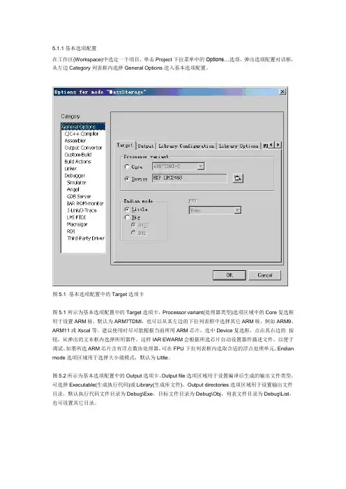
5.1.1基本选项配置在工作区(Workspace)中选定一个项目,单击Project下拉菜单中的Options…选项,弹出选项配置对话框,从左边Category列表框内选择General Options进入基本选项配置。
图5.1 基本选项配置中的Target选项卡图5.1所示为基本选项配置中的Target选项卡,Processor variant(处理器类型)选项区域中的Core复选框用于设置ARM核,默认为ARM7TDMI,也可以从其左边的下拉列表框中选择其它ARM核,例如ARM9、ARM11或Xscal等。
建议使用时尽可能根据当前所用ARM芯片,选中Device复选框,点击其右边的按钮,从弹出的文本框内选择所用器件,这样IAR EWARM会根据所选芯片自动设置器件描述文件,以便于调试。
如果所选ARM芯片含有浮点数协处理器,可在FPU下拉列表框内选取合适的浮点处理单元。
Endian mode选项区域用于选择大小端模式,默认为Little。
图5.2所示为基本选项配置中的Output选项卡。
Output file选项区域用于设置编译后生成的输出文件类型,可选择Executable(生成执行代码)或Library(生成库文件)。
Output directories选项区域用于设置输出文件目录,默认执行代码文件目录为Debug\Exe,目标文件目录为Debug\Obj,列表文件目录为Debug\List,也可设置其它目录。
图5.2基本选项配置中的Output选项卡图5.3基本选项配置中的Library Configuration选项卡图5.3所示为基本选项配置中的Library Configuration选项卡。
IAR C/C++编译器提供了DLIB库,支持ISO/ANSI C和C++以及IEEE754标准的浮点数。
通过Library下拉列表框选择希望采用的运行库。
选择None表示应用程序不链接运行库;选择Normal表示链接普通运行库,其中没有locale接口和C locale,不支持文件描述符,printf and scanf不支持多字节操作,strtod不支持十六进制浮点数操作。


ESP32-C3ESP-AT用户指南Release v2.3.0.0-esp32c3-182-g6e9756e7乐鑫信息科技2023年06月27日Table of contentsTable of contents i 1入门指南31.1ESP-AT是什么 (3)1.2硬件连接 (4)1.2.1硬件准备 (4)1.2.2ESP32-C3系列 (4)1.3下载指导 (5)1.3.1下载AT固件 (5)1.3.2烧录AT固件至设备 (7)1.3.3检查AT固件是否烧录成功 (9)2AT固件112.1发布的固件 (11)2.1.1ESP32-C3-MINI-1系列 (11)3AT命令集133.1基础AT命令 (13)3.1.1AT:测试AT启动 (13)3.1.2AT+RST:重启模块 (14)3.1.3AT+GMR:查看版本信息 (14)3.1.4AT+CMD:查询当前固件支持的所有命令及命令类型 (15)3.1.5AT+GSLP:进入Deep-sleep模式 (15)3.1.6ATE:开启或关闭AT回显功能 (16)3.1.7AT+RESTORE:恢复出厂设置 (16)3.1.8AT+UART_CUR:设置UART当前临时配置,不保存到flash (16)3.1.9AT+UART_DEF:设置UART默认配置,保存到flash (17)3.1.10AT+SLEEP:设置睡眠模式 (18)3.1.11AT+SYSRAM:查询当前剩余堆空间和最小堆空间 (20)3.1.12AT+SYSMSG:查询/设置系统提示信息 (20)3.1.13AT+SYSFLASH:查询或读写flash用户分区 (22)3.1.14AT+FS:文件系统操作 (23)3.1.15AT+RFPOWER:查询/设置RF TX Power (24)3.1.16说明 (25)3.1.17AT+SYSROLLBACK:回滚到以前的固件 (25)3.1.18AT+SYSTIMESTAMP:查询/设置本地时间戳 (25)3.1.19AT+SYSLOG:启用或禁用AT错误代码提示 (26)3.1.20AT+SLEEPWKCFG:设置Light-sleep唤醒源和唤醒GPIO (27)3.1.21AT+SYSSTORE:设置参数存储模式 (28)3.1.22AT+SYSREG:读写寄存器 (29)3.1.23AT+SYSTEMP:读取芯片内部摄氏温度值 (30)3.2Wi-Fi AT命令集 (30)3.2.1AT+CWMODE:查询/设置Wi-Fi模式(Station/SoftAP/Station+SoftAP) (31)3.2.2AT+CWSTATE:查询Wi-Fi状态和Wi-Fi信息 (32)3.2.3AT+CWJAP:连接AP (32)3.2.4AT+CWRECONNCFG:查询/设置Wi-Fi重连配置 (35)3.2.5AT+CWLAPOPT:设置AT+CWLAP命令扫描结果的属性 (36)i3.2.6AT+CWLAP:扫描当前可用的AP (37)3.2.7AT+CWQAP:断开与AP的连接 (38)3.2.8AT+CWSAP:配置ESP32-C3SoftAP参数 (38)3.2.9AT+CWLIF:查询连接到ESP32-C3SoftAP的station信息 (39)3.2.10AT+CWQIF:断开station与ESP32-C3SoftAP的连接 (40)3.2.11AT+CWDHCP:启用/禁用DHCP (40)3.2.12AT+CWDHCPS:查询/设置ESP32-C3SoftAP DHCP分配的IP地址范围 (42)3.2.13AT+CWAUTOCONN:上电是否自动连接AP (42)3.2.14AT+CWAPPROTO:查询/设置SoftAP模式下802.11b/g/n协议标准 (43)3.2.15AT+CWSTAPROTO:设置Station模式下802.11b/g/n协议标准 (44)3.2.16AT+CIPSTAMAC:查询/设置ESP32-C3Station的MAC地址 (44)3.2.17AT+CIPAPMAC:查询/设置ESP32-C3SoftAP的MAC地址 (45)3.2.18AT+CIPSTA:查询/设置ESP32-C3Station的IP地址 (46)3.2.19AT+CIPAP:查询/设置ESP32-C3SoftAP的IP地址 (47)3.2.20AT+CWSTARTSMART:开启SmartConfig (48)3.2.21AT+CWSTOPSMART:停止SmartConfig (49)3.2.22AT+WPS:设置WPS功能 (50)3.2.23AT+MDNS:设置mDNS功能 (51)3.2.24AT+CWJEAP:连接WPA2企业版AP (51)3.2.25AT+CWHOSTNAME:查询/设置ESP32-C3Station的主机名称 (53)3.2.26AT+CWCOUNTRY:查询/设置Wi-Fi国家代码 (54)3.3TCP/IP AT命令 (55)3.3.1AT+CIPV6:启用/禁用IPv6网络(IPv6) (56)3.3.2AT+CIPSTATE:查询TCP/UDP/SSL连接信息 (56)3.3.3AT+CIPSTATUS(弃用):查询TCP/UDP/SSL连接状态和信息 (57)3.3.4AT+CIPDOMAIN:域名解析 (58)3.3.5AT+CIPSTART:建立TCP连接、UDP传输或SSL连接 (58)3.3.6AT+CIPSTARTEX:建立自动分配ID的TCP连接、UDP传输或SSL连接 (62)3.3.7[仅适用数据模式]+++:退出数据模式 (62)3.3.8AT+CIPSEND:在普通传输模式或Wi-Fi透传模式下发送数据 (62)3.3.9AT+CIPSENDL:在普通传输模式下并行发送长数据 (63)3.3.10AT+CIPSENDLCFG:设置AT+CIPSENDL命令的属性 (65)3.3.11AT+CIPSENDEX:在普通传输模式下采用扩展的方式发送数据 (65)3.3.12AT+CIPCLOSE:关闭TCP/UDP/SSL连接 (66)3.3.13AT+CIFSR:查询本地IP地址和MAC地址 (67)3.3.14AT+CIPMUX:启用/禁用多连接模式 (68)3.3.15AT+CIPSERVER:建立/关闭TCP或SSL服务器 (69)3.3.16AT+CIPSERVERMAXCONN:查询/设置服务器允许建立的最大连接数 (70)3.3.17AT+CIPMODE:查询/设置传输模式 (71)3.3.18AT+SAVETRANSLINK:设置开机透传模式信息 (72)3.3.19AT+CIPSTO:查询/设置本地TCP/SSL服务器超时时间 (73)3.3.20AT+CIPSNTPCFG:查询/设置时区和SNTP服务器 (74)3.3.21AT+CIPSNTPTIME:查询SNTP时间 (75)3.3.22AT+CIPSNTPINTV:查询/设置SNTP时间同步的间隔 (76)3.3.23AT+CIUPDATE:通过Wi-Fi升级固件 (76)3.3.24AT+CIPDINFO:设置+IPD消息详情 (79)3.3.25AT+CIPSSLCCONF:查询/设置SSL客户端配置 (79)3.3.26AT+CIPSSLCCN:查询/设置SSL客户端的公用名(common name) (80)3.3.27AT+CIPSSLCSNI:查询/设置SSL客户端的SNI (81)3.3.28AT+CIPSSLCALPN:查询/设置SSL客户端ALPN (82)3.3.29AT+CIPSSLCPSK:查询/设置SSL客户端的PSK (82)3.3.30AT+CIPRECONNINTV:查询/设置Wi-Fi透传模式下的TCP/UDP/SSL重连间隔.833.3.31AT+CIPRECVMODE:查询/设置套接字接收模式 (84)3.3.32AT+CIPRECVDATA:获取被动接收模式下的套接字数据 (85)3.3.33AT+CIPRECVLEN:查询被动接收模式下套接字数据的长度 (86)3.3.34AT+PING:ping对端主机 (86)3.3.35AT+CIPDNS:查询/设置DNS服务器信息 (87)3.3.36AT+CIPTCPOPT:查询/设置套接字选项 (88)ii3.4Bluetooth®Low Energy AT命令集 (90)3.4.1AT+BLEINIT:Bluetooth LE初始化 (91)3.4.2AT+BLEADDR:设置Bluetooth LE设备地址 (92)3.4.3AT+BLENAME:查询/设置Bluetooth LE设备名称 (93)3.4.4AT+BLESCANPARAM:查询/设置Bluetooth LE扫描参数 (94)3.4.5AT+BLESCAN:使能Bluetooth LE扫描 (95)3.4.6AT+BLESCANRSPDATA:设置Bluetooth LE扫描响应 (96)3.4.7AT+BLEADVPARAM:查询/设置Bluetooth LE广播参数 (96)3.4.8AT+BLEADVDATA:设置Bluetooth LE广播数据 (98)3.4.9AT+BLEADVDATAEX:自动设置Bluetooth LE广播数据 (98)3.4.10AT+BLEADVSTART:开始Bluetooth LE广播 (99)3.4.11AT+BLEADVSTOP:停止Bluetooth LE广播 (100)3.4.12AT+BLECONN:建立Bluetooth LE连接 (100)3.4.13AT+BLECONNPARAM:查询/更新Bluetooth LE连接参数 (102)3.4.14AT+BLEDISCONN:断开Bluetooth LE连接 (103)3.4.15AT+BLEDATALEN:设置Bluetooth LE数据包长度 (103)3.4.16AT+BLECFGMTU:设置Bluetooth LE MTU长度 (104)3.4.17AT+BLEGATTSSRVCRE:GATTS创建服务 (105)3.4.18AT+BLEGATTSSRVSTART:GATTS开启服务 (106)3.4.19AT+BLEGATTSSRVSTOP:GATTS停止服务 (106)3.4.20AT+BLEGATTSSRV:GATTS发现服务 (107)3.4.21AT+BLEGATTSCHAR:GATTS发现服务特征 (108)3.4.22AT+BLEGATTSNTFY:服务器notify服务特征值给客户端 (108)3.4.23AT+BLEGATTSIND:服务器indicate服务特征值给客户端 (109)3.4.24AT+BLEGATTSSETATTR:GATTS设置服务特征值 (110)3.4.25AT+BLEGATTCPRIMSRV:GATTC发现基本服务 (111)3.4.26AT+BLEGATTCINCLSRV:GATTC发现包含的服务 (111)3.4.27AT+BLEGATTCCHAR:GATTC发现服务特征 (112)3.4.28AT+BLEGATTCRD:GATTC读取服务特征值 (113)3.4.29AT+BLEGATTCWR:GATTC写服务特征值 (114)3.4.30AT+BLESPPCFG:查询/设置Bluetooth LE SPP参数 (115)3.4.31AT+BLESPP:进入Bluetooth LE SPP模式 (116)3.4.32AT+BLESECPARAM:查询/设置Bluetooth LE加密参数 (117)3.4.33AT+BLEENC:发起Bluetooth LE加密请求 (118)3.4.34AT+BLEENCRSP:回复对端设备发起的配对请求 (119)3.4.35AT+BLEKEYREPLY:给对方设备回复密钥 (119)3.4.36AT+BLECONFREPLY:给对方设备回复确认结果(传统连接阶段) (120)3.4.37AT+BLEENCDEV:查询绑定的Bluetooth LE加密设备列表 (120)3.4.38AT+BLEENCCLEAR:清除Bluetooth LE加密设备列表 (121)3.4.39AT+BLESETKEY:设置Bluetooth LE静态配对密钥 (122)3.4.40AT+BLEHIDINIT:Bluetooth LE HID协议初始化 (122)3.4.41AT+BLEHIDKB:发送Bluetooth LE HID键盘信息 (123)3.4.42AT+BLEHIDMUS:发送Bluetooth LE HID鼠标信息 (124)3.4.43AT+BLEHIDCONSUMER:发送Bluetooth LE HID consumer信息 (125)3.4.44AT+BLUFI:开启或关闭BluFi (125)3.4.45AT+BLUFINAME:查询/设置BluFi设备名称 (126)3.4.46AT+BLEPERIODICDATA:设置Bluetooth LE周期性广播数据 (127)3.4.47AT+BLEPERIODICSTART:开启周期性广播 (128)3.4.48AT+BLEPERIODICSTOP:停止周期性广播同步 (128)3.4.49AT+BLESYNCSTART:开启同步周期性广播 (128)3.4.50AT+BLESYNCSTOP:停止周期性广播同步 (129)3.4.51AT+BLEREADPHY:查询当前连接使用的PHY (130)3.4.52AT+BLESETPHY:设置当前连接的PHY (130)3.5MQTT AT命令集 (131)3.5.1AT+MQTTUSERCFG:设置MQTT用户属性 (131)3.5.2AT+MQTTCLIENTID:设置MQTT客户端ID (132)3.5.3AT+MQTTUSERNAME:设置MQTT登陆用户名 (133)3.5.4AT+MQTTPASSWORD:设置MQTT登陆密码 (133)iii3.5.5AT+MQTTCONNCFG:设置MQTT连接属性 (134)3.5.6AT+MQTTALPN:设置MQTT应用层协议协商(ALPN) (134)3.5.7AT+MQTTCONN:连接MQTT Broker (135)3.5.8AT+MQTTPUB:发布MQTT消息(字符串) (136)3.5.9AT+MQTTPUBRAW:发布长MQTT消息 (137)3.5.10AT+MQTTSUB:订阅MQTT Topic (137)3.5.11AT+MQTTUNSUB:取消订阅MQTT Topic (138)3.5.12AT+MQTTCLEAN:断开MQTT连接 (139)3.5.13MQTT AT错误码 (139)3.5.14MQTT AT说明 (141)3.6HTTP AT命令集 (141)3.6.1AT+HTTPCLIENT:发送HTTP客户端请求 (141)3.6.2AT+HTTPGETSIZE:获取HTTP资源大小 (142)3.6.3AT+HTTPCGET:获取HTTP资源 (143)3.6.4AT+HTTPCPOST:Post指定长度的HTTP数据 (144)3.6.5AT+HTTPURLCFG:设置/获取长的HTTP URL (144)3.6.6HTTP AT错误码 (145)3.7信令测试AT命令 (146)3.7.1AT+FACTPLCP:发送长PLCP或短PLCP (146)3.8驱动AT命令 (146)3.8.1AT+DRVADC:读取ADC通道值 (146)3.8.2AT+DRVPWMINIT:初始化PWM驱动器 (147)3.8.3AT+DRVPWMDUTY:设置PWM占空比 (148)3.8.4AT+DRVPWMFADE:设置PWM渐变 (149)3.8.5AT+DRVI2CINIT:初始化I2C主机驱动 (149)3.8.6AT+DRVI2CRD:读取I2C数据 (150)3.8.7AT+DRVI2CWRDATA:写入I2C数据 (150)3.8.8AT+DRVI2CWRBYTES:写入不超过4字节的I2C数据 (151)3.8.9AT+DRVSPICONFGPIO:配置SPI GPIO (152)3.8.10AT+DRVSPIINIT:初始化SPI主机驱动 (152)3.8.11AT+DRVSPIRD:读取SPI数据 (153)3.8.12AT+DRVSPIWR:写入SPI数据 (154)3.9Web服务器AT命令 (154)3.9.1AT+WEBSERVER:启用/禁用通过Web服务器配置Wi-Fi连接 (155)3.10用户AT命令 (155)3.10.1AT+USERRAM:操作用户的空闲RAM (156)3.10.2AT+USEROTA:根据指定URL升级固件 (157)3.10.3AT+USERDOCS:查询固件对应的用户文档链接 (158)3.11AT命令分类 (159)3.12参数信息保存在flash中的AT命令 (159)3.13AT消息 (160)4AT命令示例1634.1TCP-IP AT示例 (163)4.1.1ESP32-C3设备作为TCP客户端建立单连接 (163)4.1.2ESP32-C3设备作为TCP服务器建立多连接 (165)4.1.3远端IP地址和端口固定的UDP通信 (166)4.1.4远端IP地址和端口可变的UDP通信 (168)4.1.5ESP32-C3设备作为SSL客户端建立单连接 (170)4.1.6ESP32-C3设备作为SSL服务器建立多连接 (171)4.1.7ESP32-C3设备作为SSL客户端建立双向认证单连接 (173)4.1.8ESP32-C3设备作为SSL服务器建立双向认证多连接 (175)4.1.9ESP32-C3设备作为TCP客户端,建立单连接,实现UART Wi-Fi透传 (178)4.1.10ESP32-C3设备作为TCP服务器,实现UART Wi-Fi透传 (179)4.1.11ESP32-C3设备作为softAP在UDP传输中实现UART Wi-Fi透传 (181)4.2Bluetooth LE AT示例 (183)4.2.1简介 (183)4.2.2Bluetooth LE客户端读写服务特征值 (184)iv4.2.3Bluetooth LE服务端读写服务特征值 (188)4.2.4Bluetooth LE连接加密 (193)4.2.5两个ESP32-C3开发板之间建立SPP连接,以及在UART-Bluetooth LE透传模式下传输数据 (197)4.2.6ESP32-C3与手机建立SPP连接,以及在UART-Bluetooth LE透传模式下传输数据2014.3MQTT AT示例 (203)4.3.1基于TCP的MQTT连接(需要本地创建MQTT代理)(适用于数据量少) (203)4.3.2基于TCP的MQTT连接(需要本地创建MQTT代理)(适用于数据量多) (205)4.3.3基于TLS的MQTT连接(需要本地创建MQTT代理) (206)4.3.4基于WSS的MQTT连接 (208)4.4MQTT AT连接云示例 (209)4.4.1从AWS IoT获取证书以及endpoint (210)4.4.2使用MQTT AT命令基于双向认证连接AWS IoT (210)4.5Web Server AT示例 (212)4.5.1使用浏览器进行Wi-Fi配网 (214)4.5.2使用浏览器进行OTA固件升级 (215)4.5.3使用微信小程序进行Wi-Fi配网 (222)4.5.4使用微信小程序进行OTA固件升级 (232)4.5.5ESP32-C3使用Captive Portal功能 (232)4.6HTTP AT示例 (233)4.6.1HTTP客户端HEAD请求方法 (233)4.6.2HTTP客户端GET请求方法 (234)4.6.3HTTP客户端POST请求方法(适用于POST少量数据) (235)4.6.4HTTP客户端POST请求方法(推荐方式) (236)4.6.5HTTP客户端PUT请求方法 (238)4.6.6HTTP客户端DELETE请求方法 (239)4.7Sleep AT示例 (240)4.7.1简介 (241)4.7.2在Wi-Fi模式下设置为Modem-sleep模式 (241)4.7.3在Wi-Fi模式下设置为Light-sleep模式 (243)4.7.4在蓝牙广播态下设置为Modem-sleep模式 (243)4.7.5在蓝牙连接态下设置为Modem-sleep模式 (244)4.7.6在蓝牙广播态下设置为Light-sleep模式 (245)4.7.7在蓝牙连接态下设置为Light-sleep模式 (246)4.7.8设置为Deep-sleep模式 (247)5如何编译和开发自己的AT工程2495.1编译ESP-AT工程 (249)5.1.1详细步骤 (249)5.1.2第一步:ESP-IDF快速入门 (249)5.1.3第二步:获取ESP-AT (250)5.1.4第三步:安装环境 (250)5.1.5第四步:连接设备 (250)5.1.6第五步:配置工程 (251)5.1.7第六步:编译工程 (251)5.1.8第七步:烧录到设备 (251)5.1.9build.py进阶用法 (252)5.2如何设置AT端口管脚 (252)5.2.1ESP32-C3系列 (252)5.3添加自定义AT命令 (253)5.3.1定义AT命令 (253)5.3.2注册AT命令 (255)5.3.3尝试一下吧 (255)5.3.4定义返回消息 (256)5.3.5获取命令参数 (257)5.3.6省略命令参数 (257)5.3.7阻塞命令的执行 (260)5.3.8从AT命令端口获取输入的数据 (260)v5.4如何提高ESP-AT吞吐性能 (263)5.4.1[简单]快速配置 (264)5.4.2[推荐]熟悉数据流、针对性地配置 (264)5.5如何生成出厂参数二进制文件 (267)5.5.1factory_param_type.csv (267)5.5.2factory_param_data.csv (267)5.5.3新增一个自定义模组 (268)5.5.4新增一个自定义参数 (270)5.5.5修改现有模组的出厂参数数据 (271)5.6如何自定义低功耗蓝牙服务 (273)5.6.1低功耗蓝牙服务源文件 (273)5.6.2自定义低功耗蓝牙服务 (274)5.7如何自定义分区 (276)5.7.1修改at_customize.csv (276)5.7.2生成at_customize.bin (277)5.7.3烧录at_customize.bin至ESP32-C3设备 (277)5.7.4示例 (277)5.8如何增加一个新的模组支持 (278)5.8.1在factory_param_data.csv添加模组信息 (278)5.8.2修改esp_at_module_info结构体 (279)5.8.3配置模组文件 (279)5.9SPI AT指南 (279)5.9.1简介 (280)5.9.2使用SPI AT (281)5.9.3SPI AT速率 (283)5.10如何实现OTA升级 (284)5.10.1OTA命令对比及应用场景 (284)5.10.2使用ESP-AT OTA命令执行OTA升级 (285)5.11如何更新ESP-IDF版本 (288)5.12ESP-AT固件差异 (291)5.12.1ESP32-C3系列 (291)5.13如何从GitHub下载最新临时版本AT固件 (292)5.14自定义Bluetooth LE Services工具 (293)5.14.1生成二进制文件 (298)5.14.2下载或者更新二进制文件 (298)5.15如何生成PKI文件 (300)5.15.1证书二进制文件格式 (300)5.15.2生成证书二进制文件 (301)5.15.3下载或者更新证书二进制文件 (301)5.16AT API Reference (303)5.16.1Header File (303)5.16.2Functions (303)5.16.3Structures (307)5.16.4Macros (309)5.16.5Type Definitions (309)5.16.6Enumerations (310)5.16.7Header File (312)5.16.8Functions (312)5.16.9Macros (312)6第三方定制化AT命令和固件3136.1腾讯云IoT AT命令和固件 (313)6.1.1腾讯云IoT AT命令集 (313)6.1.2Tencent Cloud IoT AT Firmware (351)7AT FAQ3537.1AT固件 (353)7.1.1我的模组没有官方发布的固件,如何获取适用的固件? (354)vi7.1.2如何获取AT固件源码? (354)7.1.3官网上放置的AT固件如何下载? (354)7.1.4如何整合ESP-AT编译出来的所有bin文件? (354)7.1.5模组出厂AT固件是否支持流控? (354)7.2AT命令与响应 (354)7.2.1AT提示busy是什么原因? (354)7.2.2AT固件,上电后发送第一个命令总是会返回下面的信息,为什么? (354)7.2.3在不同模组上的默认AT固件支持哪些命令,以及哪些命令从哪个版本开始支持?3557.2.4主MCU给ESP32-C3设备发AT命令无返回,是什么原因? (355)7.2.5ESP-AT命令是否支持ESP-WIFI-MESH? (355)7.2.6AT是否支持websocket命令? (355)7.2.7是否有AT命令连接阿里云以及腾讯云示例? (355)7.2.8AT命令是否可以设置低功耗蓝牙发射功率? (355)7.2.9如何支持那些默认固件不支持但可以在配置和编译ESP-AT工程后支持的命令?.3557.2.10AT命令中特殊字符如何处理? (355)7.2.11AT命令中串口波特率是否可以修改?(默认:115200) (355)7.2.12ESP32-C3使用AT指令进入透传模式,如果连接的热点断开,ESP32-C3能否给出相应的提示信息? (356)7.2.13ADV广播参数超过32字节之后应该如何设置? (356)7.3硬件 (356)7.3.1在不同模组上的AT固件要求芯片flash多大? (356)7.3.2AT固件如何查看error log? (356)7.3.3AT在ESP32-C3模组上的UART1通信管脚与ESP32-C3模组的datasheet默认UART1管脚不一致? (356)7.4性能 (356)7.4.1AT Wi-Fi连接耗时多少? (356)7.4.2ESP-AT固件中TCP发送窗口大小是否可以修改? (356)7.4.3ESP32-C3AT吞吐量如何测试及优化? (357)7.5其他 (357)7.5.1乐鑫芯片可以通过哪些接口来传输AT命令? (357)7.5.2ESP32-C3AT如何指定TLS协议版本? (357)7.5.3AT固件如何修改TCP连接数? (357)8Index of Abbreviations359 9关于ESP-AT363索引365索引365viiviiiTable of contents这里是乐鑫ESP-AT开发框架的文档中心。

Arctic Tern ModBMC System / PCIe Development KitUser's GuideFor System Configurationand Set UpTable of ContentsCOPYRIGHT AND DISCLAIMERS (4)SAFETY INFORMATION (5)Electrical Safety (5)Operational Safety (5)NOTICES (6)Federal Communications Commission Statement (6)Environmental Disposal Statements (6)ARCTIC TERN MODULE SPECIFICATIONS (7)SYSTEM OVERVIEW (8)Design (8)MODULE INSTALLATION AND REMOVAL (10)Module Insertion (10)Module Removal (11)HEADERS AND CONNECTORS (12)Pin Numbering Conventions (12)RTC Backup Battery Socket (13)BMC I2C Ports (14)PCIe JTAG header (15)JTAG Programming Headers (16)Power Jumpers (3.3v Aux) (17)Power Jumpers (12v) (18)Power Jumpers (3.3v Host) (19)PCI Express (20)ModBMC Socket 1 (22)Mini HDMI (26)ModBMC Socket 2 (27)Low Pin Count (LPC) (30)Flexible Service Interface (FSI) (31)PMBus (32)Card 1 COM Ports (33)GPIO Bank 1 (34)GPIO Bank 2 (35)Card 2 Console COM port (36)Card 2 Host COM port (37)BMC Firmware ROM (38)PNOR Flash ROM (39)System Fans (40)CPU fans (41)Ethernet (42)LED Displays (43)SUPPORT (44)Getting Help (44)Copyright and DisclaimersCopyright © 2017 – 2022 Raptor Computing Systems, LLC. All Rights Reserved.Product warranty or service will not be extended if: (1) the product is damaged by the consumer in any way, including any alterations that affect the operability of the feature or features being claimed under warranty and/or product service; or (2) the serial number of the product is defaced or missing. RAPTOR COMPUTING SYSTEMS, LLC PROVIDES THIS MANUAL “AS IS” WITHOUT WARRANTY OF ANY KIND, EITHER EXPRESS OR IMPLIED, INCLUDING BUT NOT LIMITED TO THE IMPLIED WARRANTIES OR CONDITIONS OF MERCHANTABILITY OR FITNESS FOR A PARTICULAR PURPOSE. IN NO EVENT SHALL RAPTOR COMPUTING SYSTEMS, LLC, ITS DIRECTORS, OFFICERS, MEMBERS, MANAGERS, EMPLOYEES OR AGENTS BE LIABLE FOR ANY INDIRECT, SPECIAL, INCIDENTAL, OR CONSEQUENTIAL DAMAGES (INCLUDING DAMAGES FOR LOSS OF PROFITS, LOSS OF BUSINESS, LOSS OF USE OR DATA, INTERRUPTION OF BUSINESS AND THE LIKE), EVEN IF RAPTOR COMPUTING SYSTEMS, LLC HAS BEEN ADVISED OF THE POSSIBILITY OF SUCH DAMAGES ARISING FROM ANY DEFECT OR ERROR IN THIS MANUAL OR PRODUCT.SPECIFICATIONS AND INFORMATION CONTAINED IN THIS MANUAL ARE FURNISHED FOR INFORMATIONAL USE ONLY, AND ARE SUBJECT TO CHANGE AT ANY TIME WITHOUT NOTICE, AND SHOULD NOT BE CONSTRUED AS A COMMITMENT BY RAPTOR COMPUTING SYSTEMS, LLC. RAPTOR COMPUTING SYSTEMS, LLC ASSUMES NO RESPONSIBILITY OR LIABILITY FOR ANY ERRORS OR INACCURACIES THAT MAY APPEAR IN THIS MANUAL, INCLUDING THE PRODUCTS AND SOFTWARE DESCRIBED IN IT.Products and corporate names appearing in this manual may or may not be registered trademarks or copyrights of their respective companies, and are used only for identification or explanation and to the owners’ benefit, without intent to infringe.Safety InformationELECTRICAL SAFETY• To reduce the risk of electric shock, disconnect the power cable before relocating or servicing the system.• When adding or removing devices to or from the system, ensure that the power cables for thedevices are unplugged before the signal cables are connected. If possible, disconnect all powercables from the existing system before you add a device.• Before connecting or removing signal cables from the motherboard, ensure that all power cables are unplugged.• Seek professional assistance before using an adapter or extension cord. These devices couldinterrupt the grounding circuit.• Make sure that your power supply is set to the correct voltage in your area. If you are not sure about the voltage of the electrical outlet you are using, contact your local power company.• If your power supply is not functioning, do not attempt to repair it. Contact a qualified servicetechnician or your retailer.OPERATIONAL SAFETY• Before installing the carrier card or connecting devices to it, carefully read any and all providedmanuals for the devices in question.• Before using the product, make sure all cables are correctly connected and the power cables arenot damaged. If you find any damage, contact your dealer immediately.• To avoid short circuits, keep paper clips, screws, staples, and other foreign metallic objects awayfrom connectors, slots, sockets and circuitry.• Avoid dust, humidity, and temperature extremes. Do not locate the product in any area where it may become wet or damp.• Place the product on a stable surface at all times.• If you encounter technical problems with the product, contact a qualified service technician or your retailer.NoticesFEDERAL COMMUNICATIONS COMMISSION STATEMENTThis device complies with Part 15 of the FCC Rules. Operation is subject to thefollowing two conditions:• This device may not cause harmful interference, and• This device must accept any interference received including interference thatmay cause undesired operation.This equipment has been tested and found to comply with the limits for a ClassB digital device, pursuant to Part 15 of the FCC Rules. These limits are designedto provide reasonable protection against harmful interference in a residentialinstallation. This equipment generates, uses and can radiate radio frequency energyand, if not installed and used in accordance with manufacturer’s instructions, maycause harmful interference to radio communications. However, there is no guaranteethat interference will not occur in a particular installation. If this equipment doescause harmful interference to radio or television reception, which can be determinedby turning the equipment off and on, the user is encouraged to try to correct theinterference by one or more of the following measures:• Reorient or relocate the receiving antenna.• Increase the separation between the equipment and receiver.• Connect the equipment to an outlet on a circuit different from that to which thereceiver is connected.• Consult the dealer or an experienced radio/TV technician for help.ENVIRONMENTAL DISPOSAL STATEMENTSDO NOT throw the system or its components in municipal waste. This product has been designed to enable proper reuse of parts and recycling. This symbol of the crossed out wheeled bin indicates that the product (electrical and electronic equipment) should not be placed in municipal waste. Check local regulations for disposal of electronic products.DO NOT throw the mercury-containing button cell battery in municipal waste. Thissymbol of the crossed out wheeled bin indicates that the battery should not beplaced in municipal waste.Arctic Tern Module SpecificationsPrimary Logic Element1x Lattice ECP5 85k LUT FPGAForm Factor ModBMC Standard (DDR4 SODIMM dimensions) Power Requirements Single 3.3V supply, < 2AMemory Type DDR3Capacity1GBOrganization2x 512MB 16-bit devices (32-bit parallel capable) Storage Type1x SPI Parallel NOR FlashTotal Capacity16MBNetworking Micrel 9021 PHY 1 GbEGraphics ITE 66121 HDMI PHY HDMI (up to 1920x1200)PCIe Lattice SERDES1x PCIe 2.0 (commercial variant)1x PCIe 1.0 (industrial variant)High Speed Interconnect Lattice SERDES2x 5.0G/s full duplex (commercial variant)2x 2.5G/s full duplex (industrial variant)Serial Host1x TTL portBMC1x TTL portRTC Epson RX8900Battery backed I2C RTCThermal Sensors Winbond W837732x I2C Thermal Sensors (single controller) GPIO ECP5 Direct I/O 3.3V TTL GPIOTI GPIO Expander2x I2C dedicated 3.3V GPIO expanders Environmental Requirements Operation: 10°C - 35°CStorage: -40°C - 70°CHumidity: 20% - 90%, non-condensing NOTE: Specifications are subject to change without notice.System OverviewDESIGNThe Arctic Tern module has been specifically designed for applications requiring high security, small form factor, and minimal power requirements. Multiple modules may be connected together for enhanced functionality, using the on-board SERDES links. The AT1PEC1 carrier card allows up to two modules to be installed, although most on-card features will function with only the first module installed.Illustration 1: Arctic Tern Block DiagramIllustration 2: Arctic Tern Dual Module PCIe Carrier Block DiagramModule Installation and RemovalMODULE INSERTIONModules are inserted at an angle, then rotated downward into the socket latches in the same manner as standard SODIMM memory modules. Module 1 must be installed before Module 2 (if applicable) due to mechanical interference between the two modules during the installation process.To install, first gently insert the module at an approximate 45 degree angle to the carrier card as shown. The module must be fully inserted to the hard stop, otherwise it will not latch during the second part of the installation process.Once inserted, carefully but firmly press the module flat toward the carrier card. Use your thumbs and press on the upper two corners of the module during this process. Installation is complete once the latches engage and the module no longer attempts to return to an angled position away from the carrier card.MODULE REMOVALModules must be removed in the reverse order to installation. Module 2 must be removed before Module 1 due to mechanical interference between the two modules during the removal process.To remove, gently spread the two black plastic socket latches on either side of the module until the module “pops” up and sits at an angle to the carrier card. Once the module is at an angle to the carrier card, grasp the module by the two short edges and gently but firmly pull the module directly away from the socket until it releases from the carrier card.CAUTION: Attempting to over-rotate or otherwise mechanically force the module away from the carrier card can result in damage to the socket and/or module. Damage caused by improper installation or removal is not covered under warranty.Headers and ConnectorsPIN NUMBERING CONVENTIONSAll headers on the AT1PEC1 follow a standard layout, with pin 1 being denoted with a white silkscreen marking. Dual row headers follow the numbering convention shown above, where all even pins are on one side of the header and all odd pins are on the other. Single row headers use a monotonically increasing pin number, starting from pin 1. Key pins are not physically present, but are still counted as pins in the numbering scheme.Illustration 3: Dual Row Header with Annotated Pins, Marker, and KeyRTC BACKUP BATTERY SOCKET376 / 377 Coin Cell Battery (+ up)BT`1Pin Function Pin Function 1+ Power2+ Power 3GroundBMC I2C PORTSJ100 (Left)Pin FPGA Pin Function1D5I2C_BMC_SCL 2-Ground3E4I2C_BMC_SDAJ101 (Middle)Pin FPGA Pin Function1B2I2C_BMC_SCL 2-Ground3B1I2C_BMC_SDAJ102 (Right)Pin FPGA Pin Function1E8I2C_BMC_SCL 2-Ground3C7I2C_BMC_SDAPCIE JTAG HEADERJ10100Pin FPGA Pin Function Pin FPGA Pin Function 1T5JTAG_TCK2V4JTAG_TDO 3R5JTAG_TDI4U5JTAG_TMS 5V3JTAG_TRST_N6-GroundJTAG PROGRAMMING HEADERSJ10107 / J10108 (Top / Bottom) (Module 1 / Module 2)Pin FPGA Pins Function Pin FPGA Pins Function1U5JTAG_TMS2R5JTAG_TDI3V4JTAG_TDO4T5JTAG_TCK5-Ground6-+3.3V Aux PowerPOWER JUMPERS (3.3V AUX)J10121 / J10122Pin Function Pin Function1PCIe connector power pins2+3.3V Aux powerPlace jumper caps across pins 1 and 2 on J10121 and J10122 to connect 3.3V Aux power to PCIe.POWER JUMPERS (12V)J10123Pin Function Pin Function1+12V power2PCIe power pinsPlace jumper cap across pins 1 and 2 to connect 12V Aux power to PCIe.POWER JUMPERS (3.3V HOST)J10120Pin Function Pin Function1+3.3V host power2PCIe connector power pinsPlace jumper cap across pins 1 and 2 to connect 3.3V Host power to PCIe.PCI EXPRESSJ13059Pin FPGA Pins Function Pin FPGA Pins FunctionB5-SMCLKA1-PRSNT1_N (Connected toPRSNT2_N)A5T5JTAG_TCK B6-SMDATA6R5JTAG_TDI B9V3JTAG_TRST_NA7V4JTAG_TDO B11EXP1/GPIO1WAKE_NA8U5JTAG_TMS B12-RSVD1 (No connect)A11A6PERST_N B14Y5PET_0_PA13Y11REFCLK_P B15Y6PET_0_NA14Y12REFCLK_N B17-PRSNT2_N (Connected toPRSNT1_N)A16W4PER_0_PA17W5PER_0_NPowerA212V Power B112V PowerA312V Power B212V PowerA9 3.3V Power B312V PowerA10 3.3V Power B8 3.3V PowerB10 3.3 Aux PowerGroundA4Ground B4GroundA12Ground B7GroundA15Ground B13GroundA18Ground B16GroundB18GroundNote: EXP0 and EXP1 are used to refer to the GPIO expanders onboard each Arctic Tern module, where EXP0 is attached to I2C bus 4 and EXP1 is attached to I2C bus 5.MODBMC SOCKET 1J13060 (Bottom)Pin FPGA Pin Function Pin FPGA Pin Function1-VDD_12V_STBY2-VDD_RGMII_REF 3-VDD3_3V_STBY4-VDD3_3V_STBY 5-VDD3_3V_STBY6-VDD3_3V_STBY 7-VDD3_3V_RTC_BATT8-Ground9-Ground10-DACG (No connect) 11-Ground12-DACB (No connect) 13A18GPIO014-DACR15B18GPIO116-HSYNC17T2GPIO318-VSYNC19T3GPIO520-DDC_CLK21C1CONSOLE_RX22-DDC_DAT23C2CONSOLE_TX24-Ground25EXP0/GPOI0GPIO726B5PWM027E1PWM228C5PWM129-PWM4 (No connect)30H3PWM331-PWM6 (No connect)32-PWM5 (No connect) 33-Ground34-PWM7 (No connect) 35EXP0/GPOI1GPIO1536EXP0/GPOI3GPIO1937EXP0/GPOI2GPIO1738EXP0/GPOI4GPIO2039-Ground40EXP0/GPOI5GPIO2141B8UART1_RX42C8UART2_RX43A7UART1_TX44D8UART2_TX45-Ground46EXP0/GPOI6GPIO2547-I2C8_SCL (No connect)48-I2C13_SCL (No connect) 49-I2C8_SDA (No connect)50-I2C13_SDA (No connect) 51-Ground52-Ground53-I2C7_SCL (No connect)54-I2C6_SCL (No connect) 55-I2C7_SDA (No connect)56-I2C6_SDA (No connect) 57-Ground58-Ground59EXP0/GPOI7GPIO3560EXP1/SCL I2C5_SCL61EXP0/GPOI8GPIO3762EXP1/SDA I2C5_SDA63E2FW_SPI_CS0#64-Ground65F2FW_SPI_IO066-HDMI_TX0_N67F3FW_SPI_IO168-HDMI_TX0_P69D1FW_SPI_IO270-HDMI_TX1_N71A2FW_SPI_IO372-HDMI_TX1_P73G3FW_SPI_CLK74EXP0/GPOI9GPIO4475-FW_SPI_CS1# (No76EXP0/GPOI10GPIO45connect)77-PWRGOOD (No connect)78D7TACH079-HDMI_TX2_N80C6TACH181-HDMI_TX2_P82E7TACH283EXP0/GPOI11GPIO5184D6TACH385-HDMI_CLK_N86A4TACH487-HDMI_CLK_P88-TACH5 (No connect)89EXP0/GPOI12GPIO5790-TACH6 (No connect)91EXP0/GPOI13GPIO5992-TACH7 (No connect)93EXP0/GPOI14GPIO6194-TACH8 (No connect)95EXP0/GPOI15GPIO6396-TACH9 (No connect)97-CPU_RST# (No connect)98-TACH10 (No connect)99EXP0/GPOI16GPIO67100-TACH11 (No connect) 101EXP0/GPOI17GPIO69102-TACH12 (No connect) 103EXP1/GPOI0GPIO71104-TACH13 (No connect) 105EXP1/GPOI1GPIO73106-TACH14 (No connect)107EXP1/GPOI2GPIO75108-TACH15 (No connect) 109EXP1/GPOI3GPIO76110-Ground113EXP1/GPOI4GPIO77114-Ground115EXP1/GPOI5GPIO79116-SPI3_CLK (No connect) 117EXP1/GPOI6GPIO81118-SPI3_MISO (No connect) 119EXP1/GPOI7GPIO83120-SPI3_MOSI (No connect) 121EXP1/GPOI8GPIO85122-SPI3_CS0# (No connect) 123B2I2C2_SCL124-SPI3_CS1# (No connect) 125B1I2C2_SDA126-Ground127-Ground128D5I2C1_SCL129-I2C14_SCL (No connect)130E4I2C1_SDA131-I2C14_SDA (No connect)132-Ground133-Ground134EXP0/SCL I2C4_SCL135-I2C16_SCL (No connect)136EXP0/SDA I2C4_SDA137-I2C16_SDA (No connect)138EXP1/GPOI9GPIO98139-Ground140EXP1/GPOI10GPIO99141T1I2C12_SCL142A6PCIE_RST#143V1I2C12_SDA144-UART3_RX145-Ground146-UART3_TX147W5PCIE_RX_N148-UART4_RX149W4PCIE_RX_P150-UART4_TX151-Ground152-VDD_LPC3V3153Y6PCIE_TX_N154EXP1/GPOI11GPIO106155Y5PCIE_TX_P156EXP1/GPOI12GPIO107157-Ground158-GPIO108 (No connect) 159Y12PCIE_CLK_N160-GPIO109 (No connect) 161Y11PCIE_CLK_P162V3JTAG_RST163-Ground164V4JTAG_TDO165C3LPC_RST#166R5JTAG_TDI167A3LPC_LAD1168T5JTAG_RTCK169C4LPC_LAD0170T5JTAG_TCK171F4LPC_IRQ#172U5JTAG_TMS173D3LPC_FRAME#175B3LPC_LAD3177B4LPC_LAD2179H5LPC_CLK181U2I2C9_SCL183R3I2C9_SDA185-Ground187-I2C10_SCL (No connect)189-I2C10_SDA (No connect)190-SPI2_CS# (No connect) 191-Ground192-SPI2_MISO (No connect) 193-I2C15_SCL (No connect)194-SPI2_MOSI (No connect) 195-I2C15_SDA (No connect)196-SPI2_CLK (No connect) 197-Ground198G5AUX_SPI_CS0#199-I2C11_SCL (No connect)COLOR CODESGPIOPWM / TACHSerial (UART)SPIHDMI / HSYNC / VSYNC / DDCI2CDACPCIELPCJTAGMINI HDMIJ13062 / J13082 (top / bottom)Pin Function Pin Function1TMDS2_GND2TMDS2_P3TMDS2_N4TMDS1_GND5TMDS1_P6TMDS1_N7TMDS0_GND8TMDS0_P9TMDS0_N10TMDS_CLK_GND 11TMDS_CLK_P12TMDS_CLK_N13DDC_CEC_GND14CEC15DDC116DDC217NC (No connect)185V19HOT_PLUG_DETS1MH1S2MH2S3MH3S4MH4MODBMC SOCKET 2J13080 (Top)Pin FPGA Pin Function Pin FPGA Pin Function1-VDD_12V_STBY2-VDD_RGMII_REF 3-VDD3_3V_STBY4-VDD3_3V_STBY 5-VDD3_3V_STBY6-VDD3_3V_STBY 7-VDD3_3V_RTC_BATT8-Ground9-Ground10-DACG (No connect) 11-Ground12-DACB (No connect) 13A18GPIO014-DACR15B18GPIO116-HSYNC17T2GPIO318-VSYNC19T3GPIO520-DDC_CLK21C1CONSOLE_RX22-DDC_DAT23C2CONSOLE_TX24-Ground25EXP0/GPOI0GPIO733-Ground35EXP0/GPOI1GPIO1536EXP0/GPOI3GPIO1937EXP0/GPOI2GPIO1738EXP0/GPOI4GPIO2039-Ground40EXP0/GPOI5GPIO2141B8UART1_RX42C8UART2_RX43A7UART2_TX44D8UART2_TX45-Ground46EXP0/GPOI6GPIO2547-I2C8_SCL (No connect)48-I2C13_SCL (No connect) 49-I2C8_SDA (No connect)50-I2C13_SDA (No connect) 51-Ground52-Ground53-I2C7_SCL (No connect)54-I2C6_SCL (No connect) 55-I2C7_SDA (No connect)56-I2C6_SDA (No connect) 57-Ground58-Ground59EXP0/GPOI7GPIO3560EXP1/SCL I2C5_SCL61EXP0/GPOI8GPIO3762EXP1/SDA I2C5_SDA64-Ground66-HDMI_TX0_N68-HDMI_TX0_P70-HDMI_TX1_N72-HDMI_TX1_P74EXP0/GPOI9GPIO4476EXP0/GPOI10GPIO45 (No connect)77-PWRGOOD (No connect) 79-HDMI_TX2_N81-HDMI_TX2_P83EXP0/GPOI11GPIO51 (No connect)85-HDMI_CLK_N87-HDMI_CLK_P89EXP0/GPOI12GPIO57 (No connect)91EXP0/GPOI13GPIO59 (No connect)93EXP0/GPOI14GPIO61 (No connect)95EXP0/GPOI15GPIO63 (No connect)97-CPU_RST# (No connect) 99EXP0/GPOI16GPIO67 (No connect)101EXP0/GPOI17GPIO69 (No connect) 103EXP1/GPOI0GPIO71 (No connect)105EXP1/GPOI1GPIO73 (No connect) 107EXP1/GPOI2GPIO75 (No connect)109EXP1/GPOI3GPIO76 (No connect) 110-Ground113EXP1/GPOI4GPIO77 (No connect) 114-Ground115EXP1/GPOI5GPIO79 (No connect) 117EXP1/GPOI6GPIO81 (No connect)119EXP1/GPOI7GPIO83 (No connect) 121EXP1/GPOI8GPIO85 (No connect)123B2I2C2_SCL125B1I2C2_SDA126-Ground127-Ground128D5I2C1_SCL129-I2C14_SCL (No connect)130E4I2C1_SDA131-I2C14_SDA (No connect)132-Ground133-Ground134EXP0/SCL I2C4_SCL135-I2C16_SCL (No connect)136EXP0/SDA I2C4_SDA137-I2C16_SDA (No connect)138EXP1/GPOI9GPIO98 (No connect) 139-Ground140EXP1/GPOI10GPIO99 (No connect) 141T1I2C12_SCL142A6PCIE_RST#143V1I2C12_SDA144-UART3_RX145-Ground146-UART3_TX147W5PCIE_RX_N148-UART4_RX149W4PCIE_RX_P150-UART4_TX151-Ground152-VDD_LPC3V3153Y6PCIE_TX_N154EXP1/GPOI11GPIO106 (No connect) 155Y5PCIE_TX_P156EXP1/GPOI12GPIO107 (No connect) 157-Ground158-GPIO108 (No connect) 159Y12PCIE_CLK_N160-GPIO109 (No connect) 161Y11PCIE_CLK_PLOW PIN COUNT (LPC)J13083Pin FPGA Pin Function Pin FPGA Pin Function1H5LPC_CLK2-Ground3D3LPC_FRAME_N4-NC2 (No connect) 5C3LPC_RESET_N6-NC1 (No connect) 7B3LPC_AD38B4LPC_AD29-3V3_AUX10A3LPC_AD111C4LPC_AD012-Ground13-TPM_SCL14-TPM_SDA15-3V3_AUX16F4LPC_SERIRQ17-Ground18-LPC_CLKRUN_N 19-WINDOW_OPEN_N20-TPM_GPIO0FLEXIBLE SERVICE INTERFACE (FSI)J200Pin FPGA Pin Function Pin Function 1T2GPIO_CARD1_32Ground 3B18GPIO_CARD1_14Ground 5A18GPIO_CARD1_0PMBUSJ201Pin Function Pin Function1T1I2C_BMC12_SCL2V1I2C_BMC12_SDA 3EXP1/GPOI0GPIO_CARD1_714-Ground5-No connectCARD 1 COM PORTSJ24 / J25 (Bottom/Top) (COM1 / COM2)Pin Function Pin Function 1COM_DCD2COM_RXD 3COM_TXD 4COM_DTR 5Ground6COM_DSR 7COM_RTS 8COM_CTS 9COM_NRIJ300Pin FPGA Pin Function Pin FPGA Pin Function1EXP1/GPOI2GPIO_CARD1_75 2EXP1/GPOI3GPIO_CARD1_76 3EXP1/GPOI4GPIO_CARD1_77 4EXP1/GPOI5GPIO_CARD1_79 5EXP1/GPOI6GPIO_CARD1_81 6EXP1/GPOI7GPIO_CARD1_83 7EXP1/GPOI8GPIO_CARD1_85 8EXP1/GPOI9GPIO_CARD1_98 9EXP1/GPOI10GPIO_CARD1_99 10EXP1/GPOI11GPIO_CARD1_106 11EXP1/GPOI12GPIO_CARD1_107 12A18GPIO_CARD2_0 13B18GPIO_CARD2_1 14T2GPIO_CARD2_3 15EXP0/GPOI0GPIO_CARD2_7 16EXP0/GPOI1GPIO_CARD2_15 17-+3.3 Aux Power18-+3.3 Aux Power19-Ground20-GroundJ301Pin FPGA Pin Function Pin FPGA Pin Function1EXP0/GPOI2GPIO_CARD2_17 2EXP0/GPOI3GPIO_CARD2_19 3EXP0/GPOI4GPIO_CARD2_20 4EXP0/GPOI5GPIO_CARD2_21 5EXP0/GPOI6GPIO_CARD2_25 6EXP0/GPOI7GPIO_CARD2_35 7EXP0/GPOI8GPIO_CARD2_37 8EXP0/GPOI9GPIO_CARD2_44 9-Ground10-Ground11-+3.3V Host Power12-+3.3V Aux Power 13-Ground14-Ground15-+12V Power16-+12V PowerCARD 2 CONSOLE COM PORTJ400Pin FPGA Pin Function1-Ground2C1CONSOLE_RX (ModBMC Socket 2) 3C2CONSOLE_TX (ModBMC Socket 2)CARD 2 HOST COM PORTJ401Pin FPGA Pin Function1-Ground2B8UART1_RX (ModBMC Socket 2) 3A7UART1_TX (ModBMC Socket 2)BMC FIRMWARE ROMJ7500Pin FPGA Pin Function Pin FPGA Pin Function1H4HOLD (Active low) / SIO32-+3.3V Aux Power 3H4RESET (Active low)4-NC1 (No connect) 5-NC26-NC37G5CS (Active low)8F5SO / SIO19Y2WP (Active low) / SIO210-Ground11-NC412-NC513-NC614-NC715E3SI / SIO016E5SCLKPNOR FLASH ROMJ7501Pin FPGA Pins Function Pin FPGA Pins Function1A2HOLD (Active low) / SIO32-+3.3V Aux Power 3A2RESET (Active low)4-NC1 (No connect) 5-NC26-NC37E2CS (Active low)8F3SO / SIO19D1WP (Active low) / SIO210-Ground11-NC412-NC513-NC614-NC715F2SI / SIO016G3SCLKSYSTEM FANSJ7900 (Left)Pin FPGA Pin Function1-Ground2-+12V Power 3E7Tachometer 4E1PWMJ7901 (Right)Pin FPGA Pin Function1-Ground2-+12V Power 3D6Tachometer 4H3PWMCPU FANSJ7902 (Left)Pin FPGA Pin Function1-Ground2-+12V Power 3D7Tachometer 4B5PWMJ7903 (Right)Pin FPGA Pin Function1-Ground2-+12V Power 3C6Tachometer 4C5PWMETHERNETJ9500Pin Function Pin Function 1TRCT32TRD3-3TRD3+4TRD2+ 5TRD2-6TRCT2 7TRCT48TRD4+ 9TRD4-10TRD1-11TRD1+12TRCT1 13 D / ORG- 14 D / GRN-15COMM16Ground 17GRN-18GRN+ 19Ground20GroundLED DISPLAYSLD1 / LD2 / LD3 / LD4 (left to right)Pin Function Pin Function1 P2N3M4I5DP6C7D8E9G10A11B12K13J14CATHODE 15H16FSupportGETTING HELPIf you require assistance operating your Arctic Tern system, you may contact Raptor Computing Systems technical support directly at ********************. Alternatively, we also have a Wiki and other support resources available online at https://; the information you require may already be available on one of these resources.。

DSP简介DSP数字信号处理(DIGITAL Signal Processing,简称DSP)是一门涉及许多学科而又广泛应用于许多领域的新兴学科。
20世纪60年代以来,随着计算机和信息技术的飞速发展,数字信号处理技术应运而生并得到迅速的发展。
数字信号处理是一种通过使用数学技巧执行转换或提取信息,来处理现实信号的方法,这些信号由数字序列表示。
在过去的二十多年时间里,数字信号处理已经在通信等领域得到极为广泛的应用。
德州仪器、FREESCALE等半导体厂商在这一领域拥有很强的实力。
DSP的发展DSP的发展历史大致可以分成四个阶段:萌芽阶段、成长阶段、成熟阶段、突破阶段。
萌芽阶段:1982年以前在这段时期里为解决Von Neumann结构在进行数字信号处理时总线和存储器之间的瓶颈效应,许多公司投入大量人力和物力开展了很多探索性的工作,研制出了一些DSP的雏形,如AMI的S2811、INTEL的2920、AT&T的DSP-1和NEC的uPD7720。
但这些产品的运算速度都太慢,而且开发工具严重不足,无法进行大规模的开发工作,还不能称作真正意义上的DSP。
第一片DSP是1982年TI公司出品的TMS320C10,它是—个16位的定点DSP,采用了哈佛(Harvard)结构,有一个乘加器和一个累加器。
TMS320C10完成—次乘加操作需要390ns,即在一秒钟的时间内可以完成250万次左右的乘加运算。
或许正是因为生产出了第一个DSP,TI公司在此后的三十几年中一直是DSP界的领军人物。
成长阶段:1982-1987年这段时间内各公司相继研制出了自己的DDSP并不断地改进。
如1985年,TI推出了TMS320C20,它具备单指令循环的硬件支持,寻址空间达到64K字,有专门的地址寄存器,一次乘加运算只需耗时200ns。
1987年,MOTOROLA公司推山了DSP56001,采用24位的数据和指令,有专门的地址寄存器,可以循环寻址,累加器有保护位,一坎乘加运算只需耗时75ns。
UM1525User manualSTM32F0DISCOVERYDiscovery kit for STM32 F0 microcontrollersIntroductionThe STM32F0DISCOVERY helps you to discover the STM32 F0 Cortex™-M0 features andto develop your applications easily. It is based on STM32F051R8T6, an STM32 F0 series32-bit ARM® Cortex™ microcontroller, and includes an ST-LINK/V2 embedded debug tool,LEDs, push buttons and a prototyping board.Figure 1.STM32F0DISCOVERYTable 1.Applicable toolsType Part numberEvaluation tools STM32F0DISCOVERYMay 2012Doc ID 022910 Rev 21/41Contents UM1525 Contents1Conventions . . . . . . . . . . . . . . . . . . . . . . . . . . . . . . . . . . . . . . . . . . . . . . . . 62Quick start . . . . . . . . . . . . . . . . . . . . . . . . . . . . . . . . . . . . . . . . . . . . . . . . . 72.1Getting started . . . . . . . . . . . . . . . . . . . . . . . . . . . . . . . . . . . . . . . . . . . . . . 72.2System requirements . . . . . . . . . . . . . . . . . . . . . . . . . . . . . . . . . . . . . . . . . 72.3Development toolchain supporting the STM32F0DISCOVERY . . . . . . . . . 72.4Order code . . . . . . . . . . . . . . . . . . . . . . . . . . . . . . . . . . . . . . . . . . . . . . . . . 7 3Features . . . . . . . . . . . . . . . . . . . . . . . . . . . . . . . . . . . . . . . . . . . . . . . . . . . 84Hardware and layout . . . . . . . . . . . . . . . . . . . . . . . . . . . . . . . . . . . . . . . . . 94.1STM32F051R8T6 microcontroller . . . . . . . . . . . . . . . . . . . . . . . . . . . . . . 124.2Embedded ST-LINK/V2 . . . . . . . . . . . . . . . . . . . . . . . . . . . . . . . . . . . . . . 144.2.1Using ST-LINK/V2 to program/debug the STM32 F0 on board . . . . . . . 154.2.2Using ST-LINK/V2 to program/debug an external STM32 application . . 164.3Power supply and power selection . . . . . . . . . . . . . . . . . . . . . . . . . . . . . . 174.4LEDs . . . . . . . . . . . . . . . . . . . . . . . . . . . . . . . . . . . . . . . . . . . . . . . . . . . . 174.5Push buttons . . . . . . . . . . . . . . . . . . . . . . . . . . . . . . . . . . . . . . . . . . . . . . 174.6JP2 (Idd) . . . . . . . . . . . . . . . . . . . . . . . . . . . . . . . . . . . . . . . . . . . . . . . . . . 174.7OSC clock . . . . . . . . . . . . . . . . . . . . . . . . . . . . . . . . . . . . . . . . . . . . . . . . 184.7.1OSC clock supply . . . . . . . . . . . . . . . . . . . . . . . . . . . . . . . . . . . . . . . . . 184.7.2OSC 32 KHz clock supply . . . . . . . . . . . . . . . . . . . . . . . . . . . . . . . . . . . 184.8Solder bridges . . . . . . . . . . . . . . . . . . . . . . . . . . . . . . . . . . . . . . . . . . . . . 194.9Extension connectors . . . . . . . . . . . . . . . . . . . . . . . . . . . . . . . . . . . . . . . . 205Connecting modules on the prototyping board . . . . . . . . . . . . . . . . . . 275.1Mikroelektronica accessory boards . . . . . . . . . . . . . . . . . . . . . . . . . . . . . 275.2ST MEMS “adapter boards”, standard DIL24 socket . . . . . . . . . . . . . . . . 305.3Arduino shield boards . . . . . . . . . . . . . . . . . . . . . . . . . . . . . . . . . . . . . . . . 33 6Mechanical drawing . . . . . . . . . . . . . . . . . . . . . . . . . . . . . . . . . . . . . . . . 36 7Electrical schematics . . . . . . . . . . . . . . . . . . . . . . . . . . . . . . . . . . . . . . . 37 2/41Doc ID 022910 Rev 2UM1525Contents 8Revision history . . . . . . . . . . . . . . . . . . . . . . . . . . . . . . . . . . . . . . . . . . . 40Doc ID 022910 Rev 23/41List of tables UM1525 List of tablesTable 1.Applicable tools. . . . . . . . . . . . . . . . . . . . . . . . . . . . . . . . . . . . . . . . . . . . . . . . . . . . . . . . . . . 1 Table 2.ON/OFF conventions . . . . . . . . . . . . . . . . . . . . . . . . . . . . . . . . . . . . . . . . . . . . . . . . . . . . . . 6 Table 3.Jumper states. . . . . . . . . . . . . . . . . . . . . . . . . . . . . . . . . . . . . . . . . . . . . . . . . . . . . . . . . . . 14 Table 4.Debug connector CN3 (SWD) . . . . . . . . . . . . . . . . . . . . . . . . . . . . . . . . . . . . . . . . . . . . . . 16 Table 5.Solder bridge settings. . . . . . . . . . . . . . . . . . . . . . . . . . . . . . . . . . . . . . . . . . . . . . . . . . . . . 19 Table 6.MCU pin description versus board function . . . . . . . . . . . . . . . . . . . . . . . . . . . . . . . . . . . . 20 Table 7.Connecting using mikroBUS™. . . . . . . . . . . . . . . . . . . . . . . . . . . . . . . . . . . . . . . . . . . . . . 27 Table 8.Connecting using IDC10. . . . . . . . . . . . . . . . . . . . . . . . . . . . . . . . . . . . . . . . . . . . . . . . . . . 28 Table 9.Connecting with a DIL24 board . . . . . . . . . . . . . . . . . . . . . . . . . . . . . . . . . . . . . . . . . . . . . 30 Table 10.Supported MEMS adapter boards . . . . . . . . . . . . . . . . . . . . . . . . . . . . . . . . . . . . . . . . . . . 32 Table 11.Connecting with Arduino shields. . . . . . . . . . . . . . . . . . . . . . . . . . . . . . . . . . . . . . . . . . . . . 33 Table 12.Document revision history . . . . . . . . . . . . . . . . . . . . . . . . . . . . . . . . . . . . . . . . . . . . . . . . . 40 4/41Doc ID 022910 Rev 2UM1525List of figures List of figuresFigure 1.STM32F0DISCOVERY. . . . . . . . . . . . . . . . . . . . . . . . . . . . . . . . . . . . . . . . . . . . . . . . . . . . . 1 Figure 2.Hardware block diagram . . . . . . . . . . . . . . . . . . . . . . . . . . . . . . . . . . . . . . . . . . . . . . . . . . . 9 Figure 3.Top layout . . . . . . . . . . . . . . . . . . . . . . . . . . . . . . . . . . . . . . . . . . . . . . . . . . . . . . . . . . . . . 10 Figure 4.Bottom layout . . . . . . . . . . . . . . . . . . . . . . . . . . . . . . . . . . . . . . . . . . . . . . . . . . . . . . . . . . . 11 Figure 5.STM32F051R8T6 package. . . . . . . . . . . . . . . . . . . . . . . . . . . . . . . . . . . . . . . . . . . . . . . . . 12 Figure 6.STM32F051R8T6 block diagram . . . . . . . . . . . . . . . . . . . . . . . . . . . . . . . . . . . . . . . . . . . . 13 Figure 7.Typical configuration . . . . . . . . . . . . . . . . . . . . . . . . . . . . . . . . . . . . . . . . . . . . . . . . . . . . . 14 Figure 8.STM32F0DISCOVERY connections image . . . . . . . . . . . . . . . . . . . . . . . . . . . . . . . . . . . . 15 Figure 9.ST-LINK connections image. . . . . . . . . . . . . . . . . . . . . . . . . . . . . . . . . . . . . . . . . . . . . . . . 16 Figure ing IDC10 and mikroBUS™ connectors. . . . . . . . . . . . . . . . . . . . . . . . . . . . . . . . . . . . . 29 Figure 11.DIL24 socket connections. . . . . . . . . . . . . . . . . . . . . . . . . . . . . . . . . . . . . . . . . . . . . . . . . . 31 Figure 12.Arduino shield board connections. . . . . . . . . . . . . . . . . . . . . . . . . . . . . . . . . . . . . . . . . . . . 35 Figure 13.STM32F0DISCOVERY mechanical drawing . . . . . . . . . . . . . . . . . . . . . . . . . . . . . . . . . . . 36 Figure 14.STM32F0DISCOVERY. . . . . . . . . . . . . . . . . . . . . . . . . . . . . . . . . . . . . . . . . . . . . . . . . . . . 37 Figure 15.ST-LINK/V2 (SWD only). . . . . . . . . . . . . . . . . . . . . . . . . . . . . . . . . . . . . . . . . . . . . . . . . . . 38 Figure 16.MCU . . . . . . . . . . . . . . . . . . . . . . . . . . . . . . . . . . . . . . . . . . . . . . . . . . . . . . . . . . . . . . . . . . 39Doc ID 022910 Rev 25/41Conventions UM1525 1 ConventionsTable 2 provides the definition of some conventions used in the present document.Table 2.ON/OFF conventionsConvention DefinitionJumper JP1 ON Jumper fittedJumper JP1 OFF Jumper not fittedSolder bridge SBx ON SBx connections closed by solderSolder bridge SBx OFF SBx connections left open6/41Doc ID 022910 Rev 2UM1525Quick startDoc ID 022910 Rev 27/412 Quick startThe STM32F0DISCOVERY is a low-cost and easy-to-use development kit to quicklyevaluate and start development with an STM32 F0 series microcontroller.Before installing and using the product, please accept the Evaluation Product License Agreement from /stm32f0discovery .For more information on the STM32F0DISCOVERY and for demonstration software, visit /stm32f0discovery .2.1 Getting startedFollow the sequence below to configure the STM32F0DISCOVERY board and launch theDISCOVER application:1.Check jumper position on the board, JP2 on, CN2 on (Discovery selected).2.Connect the STM32F0DISCOVERY board to a PC with a USB cable ‘type A to mini-B’ through USB connector CN1 to power the board. Red LED LD1 (PWR) and LD2 (COM) light up and green LED LD3 blinks.3. Press user button B1 (bottom left corner of the board).4. Observe how the green LED LD3 blinking changes according to USER button B1 clicks.5. Each click on USER button B1 is confirmed by the blue LED LD4.6. To study or modify the DISCOVER project related to this demo, visit /stm32f0discovery and follow the tutorial.7. Discover the STM32F0 features, download and execute programs proposed in the list of projects.8.Develop your own application using available examples.2.2 System requirements●Windows PC (XP , Vista, 7)●USB type A to Mini-B USB cable2.3 Development toolchain supporting the STM32F0DISCOVERY●Altium®, TASKING™ VX-toolset ●ARM®, Atollic TrueSTUDIO®●IAR™, EWARM (IAR Embedded Workbench®)●Keil™, MDK-ARM™2.4 Order codeTo order the STM32F0 Discovery kit, use the order code STM32F0DISCOVERY.Features UM15258/41Doc ID 022910 Rev 23 FeaturesThe STM32F0DISCOVERY kit offers the following features:●STM32F051R8T6 microcontroller featuring 64 KB Flash, 8 KB RAM in an LQFP64 package●On-board ST -LINK/V2 with selection mode switch to use the kit as a standalone ST -LINK/V2 (with SWD connector for programming and debugging)●Board power supply: through USB bus or from an external 5 V supply voltage ●External application power supply: 3 V and 5 V ●Four LEDs:–LD1 (red) for 3.3 V power on–LD2 (red/green) for USB communication –LD3 (green) for PC9 output –LD4 (blue) for PC8 output●Two push buttons (user and reset)●Extension header for LQFP64 I/Os for quick connection to prototyping board and easy probing.●An additional board is provided with the kit which can be connected to the extension connector for even easier prototyping and probing.●A large number of free ready-to-run application firmware examples are available on /stm32f0discovery to support quick evaluation and development.UM1525Hardware and layout 4 Hardware and layoutThe STM32F0DISCOVERY is designed around the STM32F051R8T6 microcontroller in a64-pin LQFP package.Figure 2 illustrates the connections between the STM32F051R8T6 and its peripherals (ST-LINK/V2, push button, LEDs and connectors).Figure 3 and Figure 4 help you to locate these features on the STM32F0DISCOVERY.Doc ID 022910 Rev 29/41Hardware and layout UM1525Note:Pin 1 of CN2, CN3, P1 and P2 connectors are identified by a square.10/41Doc ID 022910 Rev 2Doc ID 022910 Rev 211/4112/41Doc ID 022910 Rev 24.1 STM32F051R8T6 microcontrollerThis 32-bit low- and medium-density advanced ARM™ MCU with a high-performance ARMCortex™-M0 32-bit RISC core has 64 Kbytes Flash, 8 Kbytes RAM, RTC, timers, ADC, DAC, comparators and communication interfaces.Figure 5.STM32F051R8T6 package-3 634- & 2 4+BYTE OF &LASH MEMORY+BYTES OF 2!-,1&0 X MMThe STM32 F0 delivers 32-bit performance and STM32 DNA essentials into applications typically addressed by 8- or 16-bit microcontrollers. It benefits from the combination of real-time performance, low-power operation, advanced architecture and peripherals associated to the STM32 ecosystem, which has made the STM32 a reference in the market. Now all this is accessible for cost-sensitive applications. The STM32 F0 offers unparalleled flexibility and scalability for home entertainment products, appliances, and industrial equipment.This device provides the following benefits.●Superior code execution for better performance and excellent code efficiency for reduced embedded memory usage●High-performance connectivity and advanced analog peripherals to support a wide range of applications●Flexible clock options and low power modes with fast wake-up for low power consumptionIt has the following key features:●Core and operating conditions –ARM® Cortex™-M0 0.9 DMIPS/MHz up to 48 MHz –1.8/2.0 to3.6 V supply range ●High-performance connectivity – 6 Mbit/s USART–18 Mbit/s SPI with 4- to 16-bit data frame – 1 Mbit/s I²C fast-mode plus –HDMICEC●Enhanced control –1x 16-bit 3-phase PWM motor control timer –5x 16-bit PWM timers –1x 16-bit basic timer –1x 32-bit PWM timer –12 MHz I/O togglingDoc ID 022910 Rev 213/4114/41Doc ID 022910 Rev 24.2 Embedded ST-LINK/V2The ST -LINK/V2 programming and debugging tool is integrated on theSTM32F0DISCOVERY. The embedded ST -LINK/V2 can be used in 2 different ways according to the jumper states (see Table 3):●Program/debug the MCU on board,●Program/debug an MCU in an external application board using a cable connected to SWD connector CN3.The embedded ST -LINK/V2 supports only SWD for STM32 devices. For information about debugging and programming features refer to user manual UM1075 (ST -LINK/V2 in-circuit debugger/programmer for STM8 and STM32) which describes in detail all the ST -LINK/V2 features.Table 3.Jumper statesJumper stateDescriptionBoth CN2 jumpers ONST -LINK/V2 functions enabled for on board programming (default) Both CN2 jumpers OFFST -LINK/V2 functions enabled for application through external CN3 connector (SWD supported)4.2.1 Using ST-LINK/V2 to program/debug the STM32 F0 on boardTo program the STM32 F0 on board, simply plug in the two jumpers on CN2, as shown inFigure 8 in red, but do not use the CN3 connector as that could disturb communication withthe STM32F051R8T6 of the STM32F0DISCOVERY.Figure 8.STM32F0DISCOVERY connections imageDoc ID 022910 Rev 215/414.2.2 Using ST-LINK/V2 to program/debug an external STM32 applicationIt is very easy to use the ST-LINK/V2 to program the STM32 on an external application.Simply remove the 2 jumpers from CN2 as shown in Figure 9, and connect your applicationto the CN3 debug connector according to Table 4.Note:SB19 and SB22 must be OFF if you use CN3 pin 5 in your external application.Table 4.Debug connector CN3 (SWD)Pin CN3Designation1 VDD_TARGET VDD from application2 SWCLK SWD clock3 GND Ground4 SWDIO SWD data input/output5 NRST RESET of target MCU6 SWO ReservedFigure 9.ST-LINK connections image16/41Doc ID 022910 Rev 24.3 Power supply and power selectionThe power supply is provided either by the host PC through the USB cable, or by an external5V power supply.The D1 and D2 diodes protect the 5V and 3V pins from external power supplies:●5V and 3V can be used as output power supplies when another application board isconnected to pins P1 and P2.In this case, the 5V and 3V pins deliver a 5V or 3V power supply and powerconsumption must be lower than 100 mA.●5V can also be used as input power supplies e.g. when the USB connector is notconnected to the PC.In this case, the STM32F0DISCOVERY board must be powered by a power supply unitor by auxiliary equipment complying with standard EN-60950-1: 2006+A11/2009, andmust be Safety Extra Low Voltage (SELV) with limited power capability.4.4LEDs●LD1 PWR: Red LED indicates that the board is powered.●LD2 COM: Tricolor LED (COM) advises on the communication status as follows:–Slow blinking Red LED/Off: At power on before USB initialization–Fast blinking Red LED/Off: After the first correct communication between PC and STLINK/V2 (enumeration)–Red LED On: When initialization between PC and ST-LINK/V2 is successfully finished–Green LED On: After successful target communication initialization–Blinking Red/Green LED: During communication with target–Red LED On: Communication finished and OK–Orange LED On: Communication failure●User LD3: Green user LED connected to the I/O PC9 of the STM32F051R8T6.●User LD4: Blue user LED connected to the I/O PC8 of the STM32F051R8T6.4.5 Pushbuttons●B1 USER: User push button connected to the I/O PA0 of the STM32F051R8T6.●B2 RESET: Push button used to RESET the STM32F051R8T6.4.6 JP2(Idd)Jumper JP2, labeled Idd, allows the consumption of STM32F051R8T6 to be measured byremoving the jumper and connecting an ammeter.●Jumper on: STM32F051R8T6 is powered (default).●Jumper off: an ammeter must be connected to measure the STM32F051R8T6 current,(if there is no ammeter, the STM32F051R8T6 is not powered).Doc ID 022910 Rev 217/414.7 OSCclocksupplyclock4.7.1 OSCPF0 and PF1 can be used as GPIO or as HSE oscillator. By default these I/Os areconfigured as GPIO, so SB16 and SB17 are closed, SB18 is open and R22, R23, C13 andC14 are not populated.An external HSE clock can be provided to the MCU in three ways:●MCO from ST-LINK. From MCO of the STM32F103. This frequency cannot bechanged, it is fixed at 8 MHz and connected to PF0-OSC_IN of the STM32F051R8T6.Configuration needed:–SB16, SB18 CLOSED–R22,R23removed–SB17 OPEN●Oscillator onboard. From X2 crystal (not provided). For typical frequencies and itscapacitors and resistors, please refer to the STM32F051R8T6 Datasheet.Configuration needed:–SB16, SB17 SB18 OPEN–R22, R23, C13, C14 soldered●Oscillator from external PF0. From external oscillator through pin 7 of the P1connector. Configuration needed:–SB16, SB17 CLOSED–SB18 OPEN–R22 and R23 removed32 KHz clock supply4.7.2 OSCPC14 and PC15 can be used as GPIO or as LSE oscillator. By default these I/Os areconfigured as GPIO, so SB20 & SB21 are closed and X3, R24, R25 are not populated.An external LSE clock can be provided to the MCU in two ways:●Oscillator onboard. From X3 crystal (not provided). Configuration needed:–SB20, SB21 OPEN–C15, C16, R24 and R25 soldered.●Oscillator from external PC14. From external oscillator trough the pin 5 of P1connector. Configuration needed:–SB20, SB21 CLOSED–R24 and R25 removed18/41Doc ID 022910 Rev 2Doc ID 022910 Rev 219/414.8 Solder bridgesTable 5.Solder bridge settingsBridgeState (1) DescriptionSB16,17(X2 crystal)(2)2.OSC_IN clock comes from MCO if SB18 is ON and SB16,17 are OFFand comes from X2 if SB18 is OFF and SB16,17 are ON.OFF X2, C13, C14, R22 and R23 provide a clock. PF0, PF1 are disconnected from P1.ON PF0, PF1 are connected to P1 (R22, R23 and SB18 must not be fitted). SB6,8,10,12 (Default) ON Reserved, do not modify. SB5,7,9,11 (Reserved) OFF Reserved, do not modify.SB20,21(X3 crystal)OFF X3, C15, C16, R24 and R25 deliver a 32 KHz clock. PC14, PC15 are not connected to P1.ON PC14, PC15 are only connected to P1 (R24, R25 must not be fitted).SB4(B2-RESET) ON B2 push button is connected to the NRST pin of the STM32F051R8T6 MCU.OFF B2 push button is not connected the NRST pin of the STM32F051R8T6 MCU.SB3(B1-USER)ON B1 push button is connected to P A0. OFFB1 push button is not connected to P A0. SB1(VBA T powered from VDD) ON VBA T is permanently powered from VDD.OFF VBA T is not powered from VDD but pin3 of P1.SB14,15(RX,TX) OFF Reserved, do not modify. ON Reserved, do not modify.SB19(NRST) ON NRST signal of the CN3 connector is connected to the NRST pin of the STM32F051R8T6 MCU.OFF NRST signal of the CN3 connector is not connected to the NRST pin of the STM32F051R8T6 MCU.SB22(T_SWO) ON SWO signal of the CN3 connector is connected to PB3. OFF SWO signal is not connected.SB13(STM_RST) OFF No incidence on STM32F103C8T6 (ST -LINK/V2) NRST signal. ON STM32F103C8T6 (ST -LINK/V2) NRST signal is connected to GND. SB2(BOOT0) ON BOOT0 signal of the STM32F051R8T6 MCU is held low through a 510 Ohm pull-down resistor.OFF BOOT0 signal of the STM32F051R8T6 MCU can be set high through a 10 KOhm pull-up resistor R27 to solder.SB18(MCO)(2)ON Provides the 8 MHz for OSC_IN from MCO of STM32F103C8T6.OFFSee SB16, SB17 description.1.Default SBx state is shown in bold.20/41Doc ID 022910 Rev 24.9 Extension connectorsThe male headers P1 and P2 can connect the STM32F0DISCOVERY to a standardprototyping/wrapping board. STM32F051R8T6 GPI/Os are available on these connectors. P1 and P2 can also be probed by an oscilloscope, logical analyzer or voltmeter.Table 6.MCU pin description versus board function (page 1 of 7)MCU pinBoard functionMain function Alternate functionsLQFP64Push buttonLEDSWDOSCFree I/OPower supplyCN3P1P2BOOT0BOOT0606NRSTNRST 7RESET NRST510P A02_CTS, IN0,2_CH1_ETR, 1_INM6, 1_OUT ,TSC_G1_IO1, RTC_T AMP2, WKUP114USER15P A12_RTS, IN1, 2_CH2, 1_INP ,TSC_G1_IO2, EVENTOUT 1516P A22_TX, IN2, 2_CH3, 15_CH1, 2_INM6, 2_OUT ,TSC_G1_IO31617P A32_RX, IN3, 2_CH4, 15_CH2, 2_INP ,TSC_G1_IO4,1718UM1525Hardware and layoutDoc ID 022910 Rev 221/41P A41_NSS / 1_WS, 2_CK, IN4,14_CH1, DAC1_OUT, 1_INM4, 2_INM4,TSC_G2_IO12021P A51_SCK / 1_CK, CEC, IN5,2_CH1_ETR, (DAC2_OUT), 1_INM5, 2_INM5,TSC_G2_IO22122P A61_MISO / 1_MCK, IN6, 3_CH1, 1_BKIN, 16_CH1, 1_OUT ,TSC_G2_IO3, EVENTOUT 2223P A71_MOSI / 1_SD, IN7, 3_CH2, 14_CH1, 1_CH1N, 17_CH1, 2_OUT ,TSC_G2_IO4, EVENTOUT 2324P A81_CK, 1_CH1,EVENTOUT, MCO 4125P A91_TX, 1_CH2, 15_BKIN, TSC_G4_IO14224Table 6.MCU pin description versus board function (page 2 of 7)MCU pinBoard functionMain function Alternate functionsLQFP64Push buttonLEDSWDOSCFree I/OPower supplyCN3P1P2Hardware and layoutUM152522/41Doc ID 022910 Rev 2P A101_RX, 1_CH3, 17_BKIN, TSC_G4_IO24323P A111_CTS, 1_CH4, 1_OUT ,TSC_G4_IO3, EVENTOUT 4422P A121_RTS, 1_ETR, 2_OUT ,TSC_G4_IO4, EVENTOUT 4521P A13IR_OUT, SWDA T 46SWDIO 420P A142_TX, SWCLK 49SWCLK217P A151_NSS / 1_WS, 2_RX,2_CH1_ETR, EVENTOUT 5016PB0IN8, 3_CH3, 1_CH2N,TSC_G3_IO2, EVENTOUT 2627PB1IN9, 3_CH4, 14_CH1, 1_CH3N, TSC_G3_IO32728PB2 or NPOR (1.8V mode)TSC_G3_IO42829PB31_SCK / 1_CK, 2_CH2,TSC_G5_IO1, EVENTOUT55SWO611Table 6.MCU pin description versus board function (page 3 of 7)MCU pinBoard functionMain function Alternate functionsLQFP64Push buttonLEDSWDOSCFree I/OPower supplyCN3P1P2UM1525Hardware and layoutDoc ID 022910 Rev 223/41PB41_MISO / 1_MCK, 3_CH1,TSC_G5_IO2, EVENTOUT 5610PB51_MOSI / 1_SD, 1_SMBA, 16_BKIN, 3_CH2579PB61_SCL, 1_TX, 16_CH1N, TSC_G5_IO3588PB71_SDA, 1_RX, 17_CH1N, TSC_G5_IO4597PB81_SCL, CEC, 16_CH1, TSC_SYNC 614PB91_SDA,IR_EVENTOUT, 17_CH1, EVENTOUT 623PB102_SCL, CEC, 2_CH3, SYNC 2930PB112_SDA, 2_CH4, G6_IO1, EVENTOUT 3031PB122_NSS, 1_BKIN, G6_IO2, EVENTOUT 3332PB132_SCK, 1_CH1N, G6_IO33432Table 6.MCU pin description versus board function (page 4 of 7)MCU pinBoard functionMain function Alternate functionsLQFP64Push buttonLEDSWDOSCFree I/OPower supplyCN3P1P2Hardware and layoutUM152524/41Doc ID 022910 Rev 2PB142_MISO, 1_CH2N, 15_CH1, G6_IO43531PB152_MOSI, 1_CH3N, 15_CH1N, 15_CH2, RTC_REFIN 3630PC0IN10,EVENTOUT 811PC1IN11,EVENTOUT 912PC2IN12,EVENTOUT 1013PC3IN13,EVENTOUT 1114PC4IN14,EVENTOUT 2425PC5IN15,TSC_G3_IO12526PC63_CH13729PC73_CH23828PC83_CH339BLUE 27PC93_CH440GREEN26PC105115PC115214PC125313PC13RTC_T AMP1, RTC_TS, RTC_OUT , WKUP224Table 6.MCU pin description versus board function (page 5 of 7)MCU pinBoard functionMain function Alternate functionsLQFP64Push buttonLEDSWDOSCFree I/OPower supplyCN3P1P2UM1525Hardware and layoutDoc ID 022910 Rev 225/41PC14-OSC32_ INOSC32_IN 3OSC32_IN 5PC15-OSC32_OUT OSC32_OUT 4OSC32_OUT6PD23_ETR 5412PF0-OSC_IN OSC_IN5OSC_IN 7PF1-OSC_ OUT OSC_OUT 6OSC_OUT8PF4EVENTOUT 1819PF5EVENTOUT 1920PF62_SCL 4719PF72_SDA 4818VBA T VBA T13VDD_164VDD_232VDDA 13VSS_163VSS_231VSSA125V 13V 1VDD 5GND 22GNDGND3Table 6.MCU pin description versus board function (page 6 of 7)MCU pinBoard functionMain function Alternate functionsLQFP64Push buttonLEDSWDOSCFree I/OPower supplyCN3P1P2Hardware and layout UM152526/41Doc ID 022910 Rev 2GND9 GND3333Table 6.MCU pin description versus board function (page 7 of 7) MCU pin Board functionMain function Alternatefunctions LQFP64Push button LED SWD OSC Free I/O Power supply CN3P1 P25 Connecting modules on the prototyping boardThis section gives some examples of how to connect ready-to-use modules available fromdifferent manufacturers to the STM32F0DISCOVERY kit via the prototyping board includedin the kit.Software examples, based on the connections described below, are available at/stm32f0discovery.5.1 Mikroelektronica accessory boardsMikroelektronika, , has specified two standard connectors for theiraccessory boards, named mikroBUS™ (/mikrobus_specs.pdf) andIDC10.MikroBUS™ is a 16-pin connector to connect accessory boards very quickly and easily to amicrocontroller board through SPI, USART or I2C communications, along with additionalpins such as Analog Input, PWM and Interrupt.The set of mikroElektronika boards compatible with mikroBUS™ is called “Click boards”.IDC10 is a 10-pin connector to connect the general purpose I/O of an MCU to otheraccessory boards.The tables below are one solution for connecting mikroBUS™ and IDC boards to theSTM32F0DISCOVERY; this solution used in the different examples is available at/stm32f0discovery.Table 7.Connecting using mikroBUS™Mikroelektronica mikroBUS™STM32F0DISCOVERYPin Description Pin DescriptionAN Analog pin P A4DAC1_OUTRST Reset pin PB13GPIO OUTPUT (5V tolerant)CS SPI Chip Select line P A11GPIO OUTPUT (5V tolerant)SCK SPI Clock line PB3SPI1_SCKMISO SPI Slave Output line PB4SPI1_MISOMOSI SPI Slave Input line PB5SPI1_MOSIPWM PWM output line P A8TIM1_CH1INT Hardware Interrupt line PB12GPIO INPUT EXTI (5V tolerant)RX UART Receive line P A3USART2_RXTX UART Transmit line P A2USART2_TXSCL I2C Clock line PF6I2C2_SCLSDA I2C Data line PF7I2C2_SDA5V VCC 5V power line5V Power lineDoc ID 022910 Rev 227/41Table 8.Connecting using IDC10Mikroelektronica IDC10 connector STM32F0DISCOVERYP0GPIO PC0GPIO OUTPUT (3.3V tolerant)P1GPIO PC1GPIO OUTPUT (3.3V tolerant)P2GPIO PC2GPIO OUTPUT (3.3V tolerant)P3GPIO PC3GPIO OUTPUT (3.3V tolerant)P4GPIO PC4GPIO OUTPUT (3.3V tolerant)P5GPIO PC5GPIO OUTPUT (3.3V tolerant)P6GPIO PC6GPIO OUTPUT (5V tolerant)P7GPIO PC7GPIO OUTPUT (5V tolerant)VCC VCC 5V power line3V VDDGND Reference Ground GND VSSP0GPIO PC0GPIO OUTPUT (3.3V tolerant)P1GPIO PC1GPIO OUTPUT (3.3V tolerant)P2GPIO PC2GPIO OUTPUT (3.3V tolerant)P3GPIO PC3GPIO OUTPUT (3.3V tolerant) 28/41Doc ID 022910 Rev 2。
arm-linux学习笔记之minigui移植/u3/90065/showart_1793732.htmlminigui-1.6.10在s3c2410平台的移植开发板:SBC2410CPU:S3C2410linux-2.6.25.5fs:jffs2LCD:TFT320 X 240PC:fc8 linux-2.6.25.5(一)准备工作下载软件包libminigui-1.6.10.tar.gzmg-samples-1.6.10.tar.gzminigui-res-1.6.10.tar.gzmg-samples-str-1.6.2.tar.gz在/home/arm/创建一个minigui的目录,然后把这些载在的软件包放在该目录下,在分别解压缩。
再在/home/arm/minigui下创建一个miniguitmp的目录,用于安装编译以后的库文件。
(二)编译libminigui首先修改configure文件,在文件的开头加入交叉编译的路径CC=arm-9tdmi-linux-gnu-gccCPP=arm-9tdmi-linux-gnu-cppLD=arm-9tdmi-linux-gnu-ldAR=arm-9tdmi-linux-gnu-arRANLIB=arm-9tdmi-linux-gnu-ranlibSTRIP=arm-9tdmi-linux-gnu-strip然后执行[root@localhost libminigui-1.6.10]# ./configure --prefix=/home/arm/minigui/miniguitmp/ \--build=x86_64-linux \--host=arm-unknown-linux \--target=arm-unknown-linux[root@localhost libminigui-1.6.10]# make[root@localhost libminigui-1.6.10]# make install这个过程基本上不会有什么错误的执行make install的时候会把编译以后的资源安装到/home/arm/minigui/miniguitmp中,在这之下会有etc include lib usr几个目录产生。
“黑色经典”系列之《ARM嵌入式系统开发典型模块》《ARM嵌入式系统开发典型模块》1.1 嵌入式系统简介1.1.1 嵌入式系统的概念嵌入式系统是不同于常见计算机系统的一种计算机系统,它不以独立设备的物理形态出现,即它没有一个统一的外观,它的部件根据主体设备以及应用的需要嵌入在设备的内部,发挥着运算、处理、存储以及控制的作用。
从体系结构上看,嵌入式系统主要由嵌入式处理器、支撑硬件和嵌入式软件组成。
其中嵌入式处理器通常是单片机或微控制器;支撑硬件主要包括存储介质、通信部件和显示部件等;嵌入式软件则包括支撑硬件的驱动程序、操作系统、支撑软件以及应用中间件等。
1.1.2 嵌入式系统的结构下一如图操作系、51单片机等)流的嵌入式操视具体的ARM 芯实时应用程序变得相对容易(这一部分内容将在µC/OS-II操作系统的移植一章中详细讲述)。
这3种操作系统的特点这里只是简单的介绍,具体参见相关技术手册。
1.嵌入式系统硬件平台嵌入式系统硬件平台是整个嵌入式操作系统和应用程序运行的硬件平台,不同的应用通常有不同的硬件环境。
在嵌入式系统中硬件平台具有多样性的特点。
嵌入式系统的核心部件是各种类型的嵌入式处理器,目前据不完全统计,全世界嵌入式处理器的品种总量已经超过1 000种,流行体系结构有三十几个系列,数据总线宽度从8~32位,处理速度从0.1~2000MIPS。
按功能和内部结构等因素可以分成下面几类。
(1)嵌入式RISC微处理器RISC(Reduced Instruction Set Computer)是精简指令集计算机,RISC把着眼点放在如何《ARM嵌入式系统开发典型模块》使计算机的结构更加简单和如何使计算机的处理速度更加快速上。
RISC选取了使用频率最高的简单指令,抛弃复杂指令,固定指令长度,减少指令格式和寻址方式,不用或少用微码控制。
这些特点使得RISC非常适合嵌入式处理器。
嵌入式微控制器将整个计算机系统或者一部分集成到一块芯片中。
嵌入式微控制器一般以某一种微处理器内核为核心,比如以MIPS或ARM 核为核心,在芯片内部集成ROM、RAM、内部总线、定时/计数器、WatchDog、I/O端口、串行口等各种必要的功能和外设。
和嵌入式微处理器相比,嵌入式微控制器的最大特点是单片化,实现同样功能时系统的体积大大减小。
嵌入式微控制器的品种和数量较多,比较有代表性的通用系列包括Atmel公司A T91系列、三星公司S3C系列,Intel公司PXA25x系列等。
(2)嵌入式CISC处理器嵌入式微处理器的基础是通用计算机中的CPU在不同应用中将微处理器装配在专门设计的电路板上,只保留和嵌入式应用有关的功能,这样可以大幅度减小系统体积和功耗。
嵌入式微处理器目前主要有Intel公司x86系列、Motorola公司68000系列等。
2.嵌入式操作系统嵌入式操作系统完成系统初始化以及嵌入式应用的任务调度和控制等核心功能。
具有内核较精简、可配置、与高层应用紧密关联等特点。
嵌入式操作系统具有相对不变性。
嵌入式操作系统具有以下特点。
(1)体积小嵌入式系统有别于一般的计算机处理系统,它不具备像硬盘那样大容量的存储介质,而大多使用闪存(Flash Memory)作为存储介质。
这就要求嵌入式操作系统只能运行在有限的内存中,不能使用虚拟内存,中断的使用也受到限制。
因此,嵌入式操作系统必须结构紧凑,体积微小。
(2)实时性大多数嵌入式系统都是实时系统,而且多是强实时多任务系统,要求相应的嵌入式操作系统也必须是实时操作系统(RTOS)。
实时操作系统作为操作系统的一个重要分支已成为研究的一个热点,主要探讨实时多任务调度算法和可调度性、死锁解除等问题。
(3)特殊的开发调试环境提供完整的集成开发环境是每一个嵌入式系统开发人员所期待的。
一个完整的嵌入式系统的集成开发环境一般需要提供的工具是编译/连接器、内核调试/跟踪器和集成图形界面开发平台。
其中的集成图形界面开发平台包括编辑器、调试器、软件仿真器和监视器等。
3.嵌入式系统应用嵌入式系统应用是以嵌入式系统硬件平台的搭建、嵌入式操作系统的成功移植和运行为前提的,这一部分运行于嵌入式操作系统之上,完成特定的功能或利用操作系统提供的机制完成特定功能的嵌入式应用。
不同的系统需要设计不同的嵌入式应用程序。
如何简洁有效地使嵌入式系统能够应用于各种不同的应用环境,是嵌入式系统发展中所必须解决的关键问题。
经过不断地发展,嵌入式系统原有的3层结构逐步演化成为一种4层结构。
这个新增加的中间层次叫硬件抽象层,有时也叫板级支持包,是一个介于硬件与软件之间的中间层次。
硬件抽象层通过特定的上层接口与操作系统进行交互,向操作系统硬件的直接操作。
硬件抽象层的引入大大推动了嵌入式操作系统的通用化。
1.1.3 嵌入式系统的特点1.嵌入式系统工业的特点和要求从某种意义上来说,通用计算机行业的技术是垄断的,但嵌入式系统则不同。
嵌入式系统工业是不可垄断的高度分散的工业,充满了竞争、机遇与创新,没有哪一个系列的处理器和操作系统能够垄断全部市场,即便在体系结构上存在着主流,但各不相同的应用领域决定了不可能由少数公司、少数产品垄断全部市场。
因此嵌入式系统领域的产品和技术,必然是高度分散的,留给各个行业高新技术公司的创新余地很大。
另外,社会上的各个应用领域是不断向前发展的,要求其中的嵌入式处理器核心也同步发展,这也构成了推动嵌入式工业发展的强大动力。
嵌入式系统工业的基础是以应用为中心的“芯片”设计和面向应用的软件产品开发。
2.嵌入式系统的产品特征嵌入式系统是面向用户、面向产品、面向应用的,不能独立于应用自行发展,否则便会失去市场。
嵌入式系统的核心部件,嵌入式微处理器的功耗、体积、成本、处理能力和电磁兼容性等方面均受到应用要求的制约,这些也是各个半导体厂商之间竞争的热点。
嵌入式系统的硬件和软件设计都必须精心考虑,力争在同样的硅片面积上实现更高的性能,只有这样,才能在具体应用时对处理器的选择更具有竞争力。
嵌入式处理器要针对用户的具体需求,对芯片配置进行裁剪和添加才能达到理想的性能。
由于嵌入式系统和具体应用有机地结合在一起,具有较长的生命周期。
3.嵌入式处理器软件的特征嵌入式处理器的应用软件是实现嵌入式系统功能的关键,对嵌入式处理器系统软件和应用软件的要求也和通用计算机有所不同,主要有以下几点。
(1)软件要求固态化存储为了提高执行速度和系统可靠性,嵌入式系统中的软件一般都固化在存储器芯片或嵌入式微控制器本身中,而不是存贮于磁盘等载体中。
在基于ARM的嵌入式系统开发当中,调试成功的应用程序通常被烧写到在Flash中,并在系统上电复位后首先执行Flash中的程序,完成系统的各项初始化工作。
(2)软件代码要求高质量、高可靠性尽管半导体技术的发展使处理器速度不断提高、片上存储器容量不断增加,但在大多数应用中,存储空间仍然是宝贵的,还存在实时性的要求。
为此要求程序编写和编译工具的质量要高,以减小程序代码长度、提高执行速度。
(3)要求系统软件具有较高的实时性《ARM嵌入式系统开发典型模块》在多任务嵌入式系统中,对重要性各不相同的任务进行统筹兼顾的合理调度是保证每个任务及时执行的关键,单纯通过提高处理器速度是无法完成和没有效率的,这种任务调度只能由优化编写的系统软件来完成,因此系统软件的高实时性是基本要求。
(4)嵌入式系统开发需要开发工具和环境嵌入式系统本身不具备开发能力,即使设计完成以后用户通常也是不能对其中的程序功能进行修改的,必须有一套开发工具和环境才能进行开发,这些工具和环境一般是基于通用计算机上的软硬件设备以及逻辑分析仪、示波器等。
(5)嵌入式系统软件需要实时多任务操作系统开发平台通用计算机具有完善的操作系统和应用程序接口,是计算机基本组成不可缺少的部分,应用程序的开发以及完成后的软件都在系统软件平台上面运行,但一般不是实时的。
嵌入式系统则不同,应用程序可以没有操作系统直接在芯片上运行;但是为了合理地调度多任务、利用系统资源,用户必须自行选配实时多任务系统开发平台,这样才能保证程序执行的实时性、可靠性,并减少开发时间,保障软件质量。
(6)采用C语言是嵌入式系统开发的是最佳和最终选择由于汇编语言是一种非结构化的语言,对于大型的结构化程序设计已经不能完全胜任了。
这就要求我们采用更高级的C语言去完成这一工作。
1.1.4 嵌入式系统的发展趋势(1)提供强大的网络服务为适应嵌入式分布处理结构和应用上网需求,面向21世纪的嵌入式系统要求配备标准的一种或多种网络通信接口。
针对外部联网要求,嵌入设备必需配有通信接口,相应需要TCP/IP协议簇软件支持;由于家用电器相互关联(如防盗报警、灯光能源控制、影视设备和信息终端交换信息)及实验现场仪器的协调工作等要求,新一代嵌入式设备还需具备IEEE1394、USB、CAN、Bluetooth或IrDA通信接口,同时也需要提供相应的通信组网协议软件和物理层驱动软件。
为了支持应用软件的特定编程模式,如Web或无线Web编程模式,还需要相应的浏览器,如HTML、WML等。
(2)小型化、低成本、低功耗为满足这种特性,要求嵌入式产品设计者相应降低处理器的性能,限制内存容量和复用接口芯片。
这就相应提高了对嵌入式软件设计技术要求。
如,选用最佳的编程模型和不断改进算法,采用Java编程模式,优化编译器性能。
因此,既要软件人员有丰富经验,更需要发展先进嵌入式软件技术,如Java、Web和WAP等。
(3)人性化的人机界面嵌入式设备之所以为亿万用户乐于接受,重要因素之一是它们与使用者之间的亲和力,自然的人机交互界面,如司机操纵高度自动化的汽车主要还是通过习惯的方向盘、脚踏板和操纵杆。
人们与信息终端交互要求以GUI屏幕为中心的多媒体界面。
手写文字输入、语音拨号上网、收发电子邮件以及彩色图形、图像已取得初步成效。
目前一些先进的PDA在显示屏幕上已实现汉字写入、短消息语音发布,但离掌式语言同声翻译还有很大距离。
(4)完善的开发平台随着因特网技术的成熟、带宽的提高,ICP和ASP在网上提供的信息内容日趋丰富、应用项目多种多样,像电话手机、电话座机及电冰箱、微波炉等嵌入式电子设备的功能不再单一,电气结构也更为复杂。
为了满足应用功能的升级,设计师们一方面采用更强大的嵌入式处理器如32位、64位RISC芯片或信号处理器DSP增强处理能力;同时还采用实时多任务编程技术和交叉开发工具技术来控制功能复杂性,简化应用程序设计、保障软件质量和缩短开发周期。
1.2 最小系统结构及框图1.什么是最小系统嵌入式芯片自己是不能独立工作的,需要必要的外围芯片给它提供基本的工作条件。
一这些不可起构成了图1.2 最小系统结构框图《ARM嵌入式系统开发典型模块》1.3 最小系统的电源设计电源系统的地位十分重要,但往往设计者对电源系统的重视程度不够。