_________________General Description
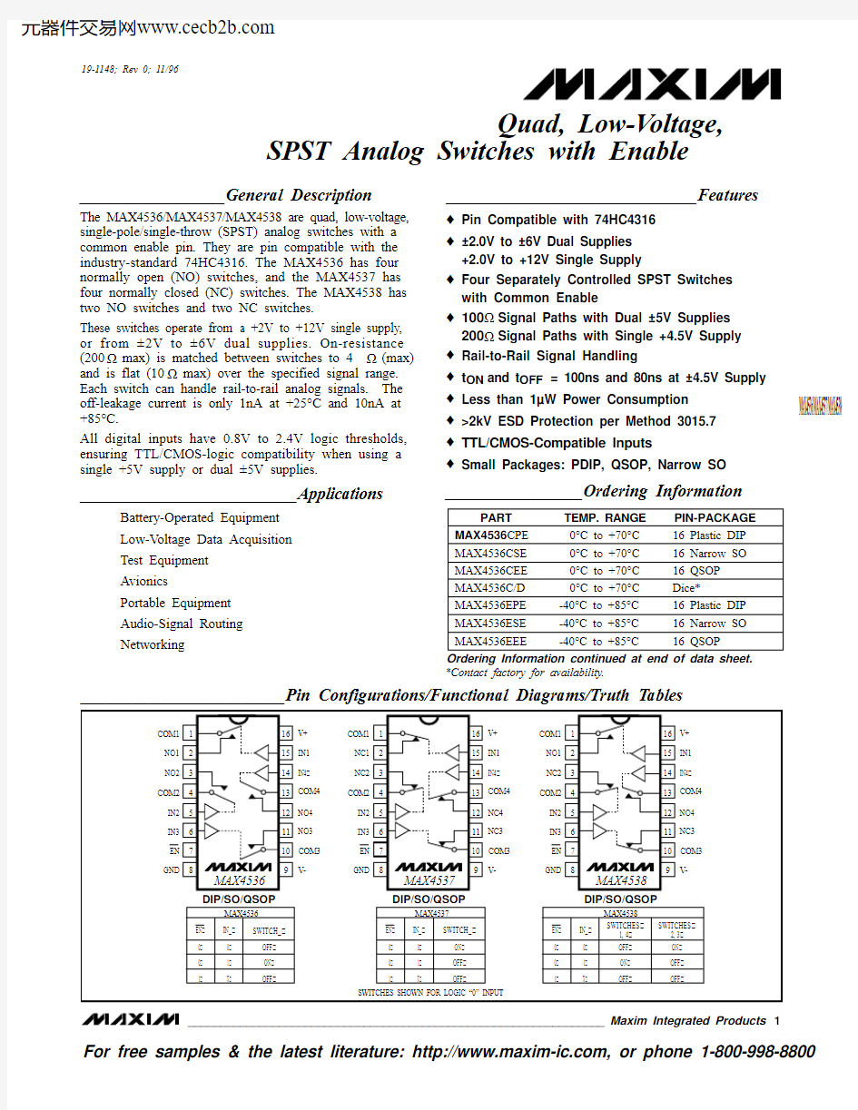
The MAX4536/MAX4537/MAX4538 are quad, low-voltage,single-pole/single-throw (SPST) analog switches with a common enable pin. They are pin compatible with the industry-standard 74HC4316. The MAX4536 has four normally open (NO) switches, and the MAX4537 has four normally closed (NC) switches. The MAX4538 has two NO switches and two NC switches.
These switches operate from a +2V to +12V single supply,or from ±2V to ±6V dual supplies. On-resistance (200?max) is matched between switches to 4?(max)and is flat (10?max) over the specified signal range.Each switch can handle rail-to-rail analog signals. The off-leakage current is only 1nA at +25°C and 10nA at +85°C.
All digital inputs have 0.8V to 2.4V logic thresholds,ensuring TTL/CMOS-logic compatibility when using a single +5V supply or dual ±5V supplies.
__________________________Applications
Battery-Operated Equipment Low-Voltage Data Acquisition Test Equipment Avionics
Portable Equipment Audio-Signal Routing Networking
______________________________Features
o Pin Compatible with 74HC4316
o ±2.0V to ±6V Dual Supplies +2.0V to +12V Single Supply
o Four Separately Controlled SPST Switches with Common Enable
o 100?Signal Paths with Dual ±5V Supplies 200?Signal Paths with Single +4.5V Supply o Rail-to-Rail Signal Handling
o t ON and t OFF = 100ns and 80ns at ±4.5V Supply o Less than 1μW Power Consumption o >2kV ESD Protection per Method 3015.7o TTL/CMOS-Compatible Inputs
o Small Packages: PDIP, QSOP, Narrow SO
MAX4536/MAX4537/MAX4538
Quad, Low-Voltage,
SPST Analog Switches with Enable
19-1148; Rev 0; 11/96
________________Ordering Information
For free samples & the latest literature: https://www.doczj.com/doc/dd19129640.html,, or phone 1-800-998-8800
M A X 4536/M A X 4537/M A X 4538
Quad, Low-Voltage,
SPST Analog Switches with Enable 2_______________________________________________________________________________________
ABSOLUTE MAXIMUM RATINGS
ELECTRICAL CHARACTERISTICS—±5V Dual Supplies
(V+ = 4.5V to 5.5V, V- = -4.5V to -5.5V, V INH = 2.4V, V INL = 0.8V, V EN = 0.8V, T A = T MIN to T MAX , unless otherwise noted. Typical values are at T A = +25°C.)
Stresses beyond those listed under “Absolute Maximum Ratings” may cause permanent damage to the device. These are stress ratings only, and functional operation of the device at these or any other conditions beyond those indicated in the operational sections of the specifications is not implied. Exposure to absolute maximum rating conditions for extended periods may affect device reliability.
Voltages Referenced to GND
V+........................................................................-0.3V to +13.0V V-.........................................................................-13.0V to +0.3V V+ to V-................................................................-0.3V to +13.0V All Other Pins (Note 1)..........................(V- -0.3V) to (V+ + 0.3V)Continuous Current into Any Terminal..............................±10mA Peak Current into Any Terminal
(pulsed at 1ms,10% duty cycle).....................................±20mA ESD per Method 3015.7.. (2000)
Continuous Power Dissipation (T A = +70°C) (Note 2)
Plastic DIP (derate 10.53mW/°C above +70°C)............842mW Narrow SO (derate 8.70mW/°C above +70°C)..............696mW QSOP (derate 8.00mW/°C above +70°C)......................800mW Operating Temperature Ranges
MAX453_C_ E.......................................................0°C to +70°C MAX453_E_ E....................................................-40°C to +85°C Storage Temperature Range.............................-65°C to +150°C Lead Temperature (soldering, 10sec).............................+300°C
Note 1:Signals on NC_, NO_, COM_, EN , or IN_ exceeding V+ or V- are clamped by internal diodes. Limit forward-diode current to
maximum current rating.
Note 2: All leads are soldered or welded to PC boards.
MAX4536/MAX4537/MAX4538
Quad, Low-Voltage,
SPST Analog Switches with Enable
_______________________________________________________________________________________3
ELECTRICAL CHARACTERISTICS—±5V Dual Supplies (continued)
(V+ = 4.5V to 5.5V, V- = -4.5V to -5.5V, V INH = 2.4V, V INL = 0.8V, V EN = 0.8V, T A = T MIN to T MAX , unless otherwise noted. Typical values are at T A = +25°C.)
M A X 4536/M A X 4537/M A X 4538
Quad, Low-Voltage,
SPST Analog Switches with Enable 4_______________________________________________________________________________________
ELECTRICAL CHARACTERISTICS—+5V Single Supply
(V+ = 4.5V to 5.5V, V- = 0V, V INH = 2.4V, V INL = 0.8V, V EN = 0.8V, T A = T MIN to T MAX , unless otherwise noted. Typical values are at T A = +25°C.)
MAX4536/MAX4537/MAX4538
Quad, Low-Voltage,
SPST Analog Switches with Enable
_______________________________________________________________________________________5
ELECTRICAL CHARACTERISTICS—+3V Single Supply
(V+ = 2.7V to 3.6V, V- = 0V, V INH = 2.0V, V INL = 0.5V, V EN = 0.5V, T A = T MIN to T MAX , unless otherwise noted. Typical values are at T A = +25°C.)
Note 3:The algebraic convention is used in this data sheet; the most negative value is shown in the minimum column.Note 4:Guaranteed by design.
Note 5:?R ON = ?R ON(MAX) - ?R ON(MIN).
Note 6:
Resistance flatness is defined as the difference between the maximum and the minimum value of on-resistance as measured over the specified analog-signal range.
Note 7:Leakage parameters are 100% tested at maximum rated hot temperature and guaranteed by correlation at
T A = +25°C.
Note 8:Off-isolation = 20log 10[V COM_/ (V NC_or V NO_)], V COM_= output, V NC_or V NO_= input to off switch.Note 9:Between any two switches.
Note 10:Leakage testing for single-supply operation is guaranteed by testing with dual supplies.
M A X 4536/M A X 4537/M A X 4538
Quad, Low-Voltage,
SPST Analog Switches with Enable 6_______________________________________________________________________________________
__________________________________________Typical Operating Characteristics
(V+ = +5V, V- = -5V GND = 0V, T A = +25°C, unless otherwise noted.)
150
501
2
5
ON-RESISTANCE vs. V COM AND TEMPERATURE (SINGLE SUPPLY)70130
V COM (V)
R O N (?)
3
4
110901406012010080
10010
±2
±3
±4
±5
ON/OFF TIME vs. SUPPLY VOLTAGE
(DUAL SUPPLIES) 2080SUPPLY VOLTAGE (V)
t O N , t O N (n s )
±6
604090705030
100.0001
-75-50-250
75100175ON/OFF LEAKAGE CURRENT vs. TEMPERATURE 0.00101.0TEMPERATURE (°C)
L E A K A G E (n A )
25501251500.10.01
1.0
0.00001
-75-50-25
75100POWER-SUPPLY CURRENT vs. TEMPERATURE 0.0001
0.1TEMPERATURE (°C)
I +, I - (μA )
25
50
125150
0.01
0.001
2000
2040-5-31
5
ON-RESISTANCE vs. V COM (DUAL SUPPLIES)
6080
100140160180120
V COM (V)
R O N (?)
-1
3
-4-22
4
80
30
-5-4
-3
-21
2
5
ON-RESISTANCE vs. V COM AND 4070V COM (V)
R O N (?)
-1
3
4
6050753565
554510,000
10
02
6
10
ON-RESISTANCE vs. V COM (SINGLE SUPPLY)
100
1000
V COM (V)
4
8
1
3
7
5
9
R O N (?)
500
-75-5025
50
150
ON/OFF TIME vs. TEMPERATURE 10
40TEMPERATURE (°C)
t O N , t O F F (n s
)
-25
7510012530
20
2
-2
-5-4
-3
-21
2
5
CHARGE INJECTION vs. V COM 0
V COM (V)
Q j , (p C )
-1
3
4
-1
1
MAX4536/MAX4537/MAX4538
Quad, Low-Voltage,
SPST Analog Switches with Enable
_______________________________________________________________________________________7
0-100
0.1
101000
1100
FREQUENCY RESPONSE
-80
FREQUENCY (MHz)
L O S S (d B )
P H A S E (D E G R E E S )
-60-40-20-10-90-70-50-3050-50-30-10103040
-40
-20020 2.5
01
2
3
6
7
10
LOGIC-LEVEL THRESHOLD vs. POSITIVE SUPPLY VOLTAGE 1.5
M A X 4536/37/38 T O C -11
SUPPLY VOLTAGE (V)
L O G I C -L E V E L T H R E S H O L D (V )
4
5
8
9
2.00.5
1.0
100
0.01
10
1k 100k
100
10k
TOTAL HARMONIC
DISTORTION vs. FREQUENCY
0.1
FREQUENCY (Hz)
T H D (%)
10
1
_____________________________Typical Operating Characteristics (continued)
(V+ = +5V, V- = -5V GND = 0V, T A = +25°C, unless otherwise noted.)
______________________________________________________________Pin Description
*NO_/NC_ and COM_ pins are identical and interchangeable. Either may be considered as an input or an output; signals pass equally well in either direction.
M A X 4536/M A X 4537/M A X 4538
__________Applications Information
Power-Supply Considerations
Overview
The MAX4536/MAX4537/MAX4538 construction is typi-cal of most CMOS analog switches. These devices have three supply pins: V+, V-, and GND. V+ and V- drive the internal CMOS switches and set the limits of the analog voltage on any switch. Reverse ESD-protection diodes are internally connected between each analog-signal pin, and both V+ and V-. One of these diodes conducts if any analog signal exceeds V+ or V-. These reverse-biased ESD diodes leak during normal operation, form-ing the only current drawn from V+ or V-.
Virtually all the analog leakage current is through the ESD diodes. Although the ESD diodes on a given sig-nal pin are identical and therefore fairly well balanced,they are reverse biased differently. Each is biased by either V+ or V- and the analog signal. This means their leakages vary as the signal varies. The difference in the two diode leakages from the signal path to the V+ and V- pins constitutes the analog-signal path leakage cur-rent. All analog leakage current flows to the supply ter-minals, not to the other switch terminal. This explains how both sides of a given switch can show leakage currents of either the same or opposite polarity.
There is no connection between the analog-signal paths and GND. The analog-signal paths consist of an N-channel and P-channel MOSFET with their sources and drains paralleled and their gates driven out of phase to V+ and V- by the logic-level translators.
V+ and GND power the internal logic and logic-level translators and set the input logic thresholds. The logic-level translators convert the logic levels to switched V+ and V- signals to drive the analog switch-es’ gates. This drive signal is the only connection between the logic supplies and the analog supplies.V+, and V- have ESD-protection diodes to GND. The logic-level inputs have ESD protection to V+ and to V-.Increasing V- has no effect on the logic-level thresh-olds, but it does increase the drive to the P-channel switches, reducing their on-resistance. V- also sets the negative limit of the analog-signal voltage.
The logic-level thresholds are CMOS/TTL-compatible when V+ is +5V. The threshold increases slightly as V+is raised. When V+ reaches +12V, the level threshold is about 3.1V, above the TTL output high-level minimum of 2.8V, but still compatible with CMOS outputs.
Bipolar Supplies
The MAX4536/MAX4537/MAX4538 operate with bipolar supplies between ±2.0V and ±6V. The V+ and V- sup-plies need not be symmetrical, but their sum cannot exceed the absolute maximum rating of 13.0V. Do not connect the MAX4536/MAX4537/MAX4538’s V+ to +3V and then connect the logic-level input pins to TTL logic-level signals. TTL logic-level outputs in excess of the absolute maximum ratings can dam-age the part and/or external circuits.
CAUTION:The absolute maximum V+ to V- differen-tial voltage is 13.0V. Typical ±6V or +12V supplies with ±10% tolerances can be as high as 13.2V. This voltage can damage the MAX4536/MAX4537/MAX4538.Even ±5% tolerance supplies may have overshoot or noise spikes that exceed 13.0V.
Single Supplies
The MAX4536/MAX4537/MAX4538 operate from single supplies between +2.0V and +12V when V- is connect-ed to GND. All of the bipolar precautions must be observed.
High-Frequency Performance
In 50?systems, signal response is reasonably flat up to 50MHz (see Typical Operating Characteristics ).Above 20MHz, the on-response has several minor peaks that are highly layout dependent. The problem with high-frequency operation is not in turning the switch on, but in turning it off. The off-state switch acts like a capacitor and passes higher frequencies with less attenuation. At 10MHz, off-isolation is about -44dB in 50?systems, becoming worse (approximately 20dB per decade) as frequency increases. Higher circuit impedances also make off-isolation worse. Adjacent channel attenuation is about 3dB above that of a bare IC socket, and is due entirely to capacitive coupling.
Quad, Low-Voltage,
SPST Analog Switches with Enable 8_______________________________________________________________________________________
MAX4536/MAX4537/MAX4538
Quad, Low-Voltage,
SPST Analog Switches with Enable
_______________________________________________________________________________________
9
Figure 3. Charge Injection
Figure 1. Switching Time
Figure 2. Break-Before-Make Interval (MAX4538 only)
______________________________________________Test Circuits/Timing Diagrams
M A X 4536/M A X 4537/M A X 4538
Quad, Low-Voltage,
SPST Analog Switches with Enable 10______________________________________________________________________________________
Figure 5. Crosstalk
Figure 4. Off Isolation
Figure 7. Channel-On Capacitance
Figure 6. Channel-Off Capacitance
MAX4536/MAX4537/MAX4538
Quad, Low-Voltage,
SPST Analog Switches with Enable
______________________________________________________________________________________11
*Contact factory for availability.
__Ordering Information (continued)
_____________________Chip Topography
MAX4536MAX4537MAX4538PIN NAME PIN NAME PIN NAME A NO1A NC1A NO1B NO2B NC2B NC2C NO3C NC3C NC3D
NO4
D
NC4
D
NO4
TRANSISTOR COUNT: 121
SUBSTRATE IS INTERNALLY CONNECTED TO V+
IN4
A
COM1IN1
COM4
D
C
0.054" (1.37mm)
0.053" (1.35mm)
EN GND V-COM3
B
COM2IN2
IN3
V+
M A X 4536/M A X 4537/M A X 4538
Quad, Low-Voltage,
SPST Analog Switches with Enable implied. Maxim reserves the right to change the circuitry and specifications without notice at any time.
12__________________Maxim Integrated Products, 120 San Gabriel Drive, Sunnyvale, CA 94086 (408) 737-7600?1996 Maxim Integrated Products
Printed USA
is a registered trademark of Maxim Integrated Products.
________________________________________________________Package Information