硅片行业术语大全(中英文对照+A-H)
- 格式:docx
- 大小:17.69 KB
- 文档页数:3

半导体行业英文术语English:Some common terms in the semiconductor industry include:1. Integrated Circuit (IC): A small electronic device made out of a semiconductor material that can perform an extensive range of functions.2. Semiconductor manufacturing: The process of creating integrated circuits and semiconductor devices, including design, fabrication, and packaging.3. Wafer: A thin slice of semiconductor material used as the substrate for the fabrication of integrated circuits.4. Photolithography: A process used to transfer circuit patterns onto the wafer surface using light and photoresist materials.5. Die: A single piece of an integrated circuit, typically cut from a wafer after fabrication and packaging.6. Yield: The percentage of functional and operational semiconductor devices produced during the manufacturing process.7. Moore's Law: The observation that the number of transistors in a dense integrated circuit doubles approximately every two years, leading to exponential growth in processing power.8. Quantum tunneling: A phenomenon in which electrons penetrate through a potential barrier they classically shouldn't be able to cross, crucial for the operation of semiconductor devices.中文翻译:半导体行业的一些常见术语包括:1. 集成电路(IC):由半导体材料制成的小型电子器件,可执行广泛的功能。
1. acceptance testing (WAT:wafer acceptance testing)2。
acceptor: 受主,如B,掺入Si中需要接受电子3。
ACCESS:一个EDA(Engineering Data Analysis)系统4。
Acid:酸5. Active device:有源器件,如MOS FET(非线性,可以对信号放大)6。
Align mark(key):对位标记7。
Alloy:合金8。
Aluminum:铝9. Ammonia:氨水10。
Ammonium fluoride:NH4F11。
Ammonium hydroxide:NH4OH12。
Amorphous silicon:α-Si,非晶硅(不是多晶硅)13。
Analog:模拟的14。
Angstrom:A(1E—10m)埃15. Anisotropic:各向异性(如POLY ETCH)16。
AQL(Acceptance Quality Level):接受质量标准,在一定采样下,可以95%置信度通过质量标准(不同于可靠性,可靠性要求一定时间后的失效率)17。
ARC(Antireflective coating):抗反射层(用于METAL等层的光刻)18. Antimony(Sb)锑19. Argon(Ar)氩20. Arsenic(As)砷21. Arsenic trioxide(As2O3)三氧化二砷22。
Arsine(AsH3)23。
Asher:去胶机24. Aspect ration:形貌比(ETCH中的深度、宽度比)25。
Autodoping:自搀杂(外延时SUB的浓度高,导致有杂质蒸发到环境中后,又回掺到外延层)26。
Back end:后段(CONTACT以后、PCM测试前)27。
Baseline:标准流程28. Benchmark:基准29。
Bipolar:双极30. Boat:扩散用(石英)舟31. CD:(Critical Dimension)临界(关键)尺寸。
金属前介质层(PMD)金属间介质层(IMD)W塞(W PLUG)钝化层(Passivation)acceptor 受主,如B,掺入Si中需要接受电子Acid:酸actuator激励ADI After develop inspection显影后检视AEI After etching inspection蚀科后检查AFM atomic force microscopy 原子力显微ALD atomic layer deposition 原子层淀积Align mark(key):对位标记Alignment 排成一直线,对平Alloy:合金Aluminum:铝Ammonia:氨水Ammonium fluoride:NHFAmmonium hydroxide:NHOHAmorphous silicon:α-Si,非晶硅(不是多晶硅) amplifier 放大器AMU 原子质量数Analog:模拟的analyzer magnet 磁分析器Angstrom:A(E-m)埃Anisotropic:各向异性(如POLY ETCH)Antimony(Sb)锑arc chamber 起弧室ARC: anti-reflect coating 防反射层Argon(Ar)氩Arsenic trioxide(AsO)三氧化二砷Arsenic(As)砷Arsine(AsH)ASHER 一种干法刻蚀方式Asher:去胶机ASI 光阻去除后检查ASIC 特定用途集成电路Aspect ration:形貌比(ETCH中的深度、宽度比) ATE 自动检测设备Back end:后段(CONTACT以后、PCM测试前)Backside Etch 背面蚀刻Backside 晶片背面Baseline:标准流程Beam-Current 电子束电流Benchmark:基准BGA ball grid array 高脚封装Bipolar:双极Boat:扩散用(石英)舟Cassette 装晶片的晶舟CD:critical dimension 关键性尺寸,临界尺寸Chamber 反应室Chart 图表Child lot 子批chiller 制冷机Chip (die) 晶粒Chip:碎片或芯片。
太阳能产业行业术语光伏产业链PV industry chain多晶硅原料-----单晶硅棒----单晶硅片----晶体硅电池----电池封装----系统集成----工程安装polycrystalline silicon raw material ---mono-crystalline silicon ingot---mono-crystalline silicon wafer---crystalline silicon cell—cells encapsulation---system integration---construction installation单词:1.单晶硅片mono-crystalline silicon wafer多晶硅片polycrystalline silicon wafer晶向orientation少数载流子寿命lifetime导电类型conductivity type位错密度dislocation硅单晶片厚度thickness硅单晶片的弯曲度surface camber准方单晶硅片: quasi-square mono-crystalline silicon wafer2.太阳电池solar cell3.薄膜太阳电池film solar cell4.光电转换photo-electricity conversion5.太阳电池组件solar module多晶硅太阳电池组件polycrystalline solar module单晶硅太阳电池组件mono-crystalline solar module6.太阳能户用系统solar home system(分为:太阳能直流户用系统;太阳能交流户用系统;太阳能交直流户用系统)7.太阳能电站solar power station(分为:离网型太阳能电站off-grid solar power station ;并网型太阳能电站grid-connected solar power station )8.太阳能热水器solar water heater9.太阳能热水系统:solar heating system10.太阳能直流式热水系统: solar direct heating system11.太阳能强迫循环热水系统solar compelling cycle heating system12.太阳能自然循环热水系统solar spontaneously cycle heating system13.真空管太阳能集热器vacuum tube solar centralized heating system14.平板型太阳能集热器flat type solar centralized heating system15.全玻璃真空太阳能集热器full-glass vacuum solar centralizedheating system16.热管式真空管太阳集热器heat-tube vacuum solar centralizedheating system17.采光面积: lighting area18.太阳能幅照度solar radiant intensity19.太阳能控制器:solar controller20.太阳能逆变器:solar inverter21.太阳能通讯基站solar telecommunication power systems22.石油和天然气管道太阳能阴极保护电站:solar power stations forcathode protection of the oil and gas feeding pipes23.太阳能电池方阵solar array24.太阳能通讯电源solar communication power station25.太阳能自动跟踪装置solar automatic tracker26.太阳能移动电源车(站)solar mobile electrical vehicle (station)27.光伏水泵solar pump28.太阳能杨水系统solar pumping system29.光—网---柴互补系统complementary system for solar –grid-dieseloil30.风---光互补系统complementary system for solar - wind31.太阳能交通信号灯solar traffic signal light32.太阳能交通警示标志solar traffic warning symbol33.太阳能道钉solar road mark34.太阳能庭院灯solar garden light35.太阳能路灯solar street light36.太阳能草坪灯solar lawn light37.太阳能广告牌solar billboard38.太阳能电话亭solar telephone booth短语:太阳能扬水和照明综合应用系统:the comprehensive utilization system of solar pumping and lighting变频调速交流异步电机:high-efficient frequency conversion alternating asynchronous motors(这个产品不是太阳能产品)送电到乡: Power Supply to Township丝绸之路光明工程:Silk Road Brightness Project太阳能亮化工程solar brightness project太阳能与建筑一体化integrate solar energy with building。
MFG 常用英文单字Semiconductor半导体导体、绝缘体和半导体主要依据导电系数的大小,决定了电子的移动速度。
导体:金、银、铜、铁、人、水……导电系数大,传导容易绝缘体:塑料、木头、皮革、纸……导电系数小、传导不容易半导体:硅中加锗、砷、镓、磷……平时不导电加特定电压后导电Wafer 芯片或晶圆:原意为法国的松饼,饼干上有格子状的饰纹,与FAB内生产的芯片图形类似.Lot 批;一批芯片中最多可以有25片,最少可以只有一片。
ID Identification的缩写.用以辨识各个独立的个体,就像公司内每一个人有自己的识别证。
Wafer ID 每一片芯片有自己的芯片刻号,叫Wafer ID.Lot ID 每一批芯片有自己的批号,叫Lot ID。
Part ID 各个独立的批号可以共享一个型号,叫Part ID。
WIP Work In Process,在制品。
从芯片投入到芯片产品,FAB内各站积存了相当数量的芯片,统称为FAB内的WIP .一整个制程又可细分为数百个Stage和Step,每一个Stage所堆积的芯片,称为Stage WIP。
Lot Priority 每一批产品在加工的过程中在WIP中被选择进机台的优先级。
Super Hot Run的优先级为1,视为等级最高,必要时,当Lot在上一站加工时,本站便要空着机台等待Super Hot Run。
Hot Run的优先级为2,紧急程度比Super Hot Run次一级.Normal的优先级为3,视为正常的等级,按正常的派货原则,或视常班向生产指令而定.Cycle time 生产周期,FAB Cycle Time 定义为:从芯片投入到芯片产生的这一段时间。
Stage Cycle Time:Lot从进站等候开始到当站加工后出货时间点截止。
Spec。
规格Specification的缩写.产品在机台加工过程中,每一站均设定规格。
机台加工后,产品或控片经由量测机台量测,该产品加工后,是否在规格内。
太阳电池 solar cell通常是指将太阳光能直接转换成电能的一种器件。
硅太阳电池silicon solar cell硅太阳电池是以硅为基体材料的太阳电池。
单晶硅太阳电池single crystalline silicon solar cell单晶硅太阳电池是以单晶硅为基体材料的太阳电池。
非晶硅太阳电池(a—si太阳电池)amorphous silicon solar cell用非晶硅材料及其合金制造的太阳电池称为非晶硅太阳电池,亦称无定形硅太阳电池,简称a—si太阳电池。
多晶硅太阳电池polycrystalline silicon solar cell多晶硅太阳电池是以多晶硅为基体材料的太阳电池。
聚光太阳电池组件photovoltaic concentrator module系指组成聚光太阳电池,方阵的中间组合体,由聚光器、太阳电池、散热器、互连引线和壳体等组成。
电池温度cell temperature系指太阳电池中P-n结的温度。
太阳电池组件表面温度solar cell module surface temperature系指太阳电池组件背表面的温度。
大气质量(AM)Air Mass (AM)直射阳光光束透过大气层所通过的路程,以直射太阳光束从天顶到达海平面所通过的路程的倍数来表示。
太阳高度角 solar 太阳高度角 solar elevation angle太阳光线与观测点处水平面的夹角,称为该观测点的太阳高度角。
辐照度 irradiance系指照射到单位表面积上的辐射功率(W/m2)。
总辐照(总的太阳辐照)total irradiation (total insolation)在一段规定的时间内,(根据具体情况而定为每小时,每天、每周、每月、每年)照射到某个倾斜表面的单位面积上的太阳辐照。
直射辐照度direct irradiance照射到单位面积上的,来自太阳圆盘及其周围对照射点所张的圆锥半顶角为8o的天空辐射功率。
硅片行业术语大全(中英文对照 I-Z)Ingot - A cylindrical solid made of polycrystalline or single crystal silicon from which wafer s are cut.晶锭 - 由多晶或单晶形成的圆柱体,晶圆片由此切割而成。
Laser Light-Scattering Event - A signal pulse that locates surface imperfections on a wafer.激光散射 - 由晶圆片表面缺陷引起的脉冲信号。
Lay - The main direction of surface texture on a wafer.层 - 晶圆片表面结构的主要方向。
Light Point Defect (LPD) (Not preferred; see localized light-scatterer) 光点缺陷(LPD) (不推荐使用,参见“局部光散射”)Lithography - The process used to transfer patterns onto wafer s.光刻 - 从掩膜到圆片转移的过程。
Localized Light-Scatterer - One feature on the surface of a wafer, such as a pit or a scratch that scatters light. It is also called a light point defect.局部光散射 - 晶圆片表面特征,例如小坑或擦伤导致光线散射,也称为光点缺陷。
Lot - Wafer s of similar sizes and characteristics placed together in a shipment.批次 - 具有相似尺寸和特性的晶圆片一并放置在一个载片器内。
太阳电池 solar cell通常是指将太阳光能直接转换成电能的一种器件。
硅太阳电池silicon solar cell硅太阳电池是以硅为基体材料的太阳电池。
单晶硅太阳电池single crystalline silicon solar cell单晶硅太阳电池是以单晶硅为基体材料的太阳电池。
非晶硅太阳电池(a—si太阳电池)amorphous silicon solar cell用非晶硅材料及其合金制造的太阳电池称为非晶硅太阳电池,亦称无定形硅太阳电池,简称a—si太阳电池。
多晶硅太阳电池polycrystalline silicon solar cell多晶硅太阳电池是以多晶硅为基体材料的太阳电池。
聚光太阳电池组件photovoltaic concentrator module系指组成聚光太阳电池,方阵的中间组合体,由聚光器、太阳电池、散热器、互连引线和壳体等组成。
电池温度cell temperature系指太阳电池中P-n结的温度。
太阳电池组件表面温度solar cell module surface temperature系指太阳电池组件背表面的温度。
大气质量(AM)Air Mass (AM)直射阳光光束透过大气层所通过的路程,以直射太阳光束从天顶到达海平面所通过的路程的倍数来表示。
太阳高度角 solar 太阳高度角 solar elevation angle太阳光线与观测点处水平面的夹角,称为该观测点的太阳高度角。
辐照度 irradiance系指照射到单位表面积上的辐射功率(W/m2)。
总辐照(总的太阳辐照)total irradiation (total insolation)在一段规定的时间内,(根据具体情况而定为每小时,每天、每周、每月、每年)照射到某个倾斜表面的单位面积上的太阳辐照。
直射辐照度direct irradiance照射到单位面积上的,来自太阳圆盘及其周围对照射点所张的圆锥半顶角为8o的天空辐射功率。
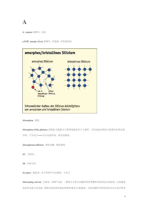
AA, Ampere的缩写, 安培a-Si:H, amorph silicon的缩写, 含氢的, 非结晶性硅.Absorption, 吸收.Absorption of the photons:光吸收;当能量大于禁带宽度的光子入射时,太阳电池内的电子能量从价带迁到导带,产生电子——空穴对的作用,称为光吸收。
Absorptionscoefficien t, 吸收系数, 吸收强度.AC, 交流电.Ah, 安培小时.Acceptor, 接收者, 在半导体中可以接收一个电子.Alternating current, 交流电,简称“交流. 一般指大小和方向随时间作周期性变化的电压或电流. 它的最基本的形式是正弦电流. 我国交流电供电的标准频率规定为50赫兹。
交流电随时间变化的形式可以是多种多样的。
不同变化形式的交流电其应用范围和产生的效果也是不同的。
以正弦交流电应用最为广泛,且其他非正弦交流电一般都可以经过数学处理后,化成为正弦交流电的迭加。
AM, air mass的缩写, 空气质量.直射阳光光束透过大气层所通过的路程,以直射太阳光束从天顶到达海平面所通过的路程的倍数来表示。
当大气压力P=1.013巴,天空无云时,海平面处的大气质量为1。
amorphous silicon solar cell:非晶硅太阳电池(a—si太阳电池)用非晶硅材料及其合金制造的太阳电池称为非晶硅太阳电池,亦称无定形硅太阳电池,简称a—si太阳电池。
Angle of inclination, 倾斜角,即电池板和水平方向的夹角,0-90度之间。
Anode, 阳极, 正极.BBack Surface Field, 缩写BSF, 在晶体太阳能电池板背部附加的电子层, 来提高电流值.Bandbreak, 在半导体中, 价带和导带之间的空隙,对于半导体的吸收特性有重要意义.Becquerel, Alexandre-Edmond, 法国物理学家, 在1839年发现了电池板效应.BSF, back surface field的缩写.Bypas-Diode, 与太阳能电池并联的二极管, 当一个太阳能电池被挡住, 其他太阳能电池产生的电流可以从它处通过.CCadmium-Tellurid, 缩写CdTe; 位于II/VI位的半导体, 带空隙值为1,45eV, 有很好的吸收性, 应用于超薄太阳能电池板, 或者是连接半导体.Cathode, 阴极,或负极,是在电池板电解液里的带负电的电极,是电池板电解液里带电粒子和导线里导电电子的过渡点。
硅片行业术语大全中英文对照I-Z硅片行业术语大全(中英文对照 I-Z)Ingot - A cylindrical solid made of polycrystalline or single crystal silicon from which wafer s are cut.晶锭 - 由多晶或单晶形成的圆柱体,晶圆片由此切割而成。
Laser Light-Scattering Event - A signal pulse that locates surface imperfections on a wafer.激光散射 - 由晶圆片表面缺陷引起的脉冲信号。
Lay - The main direction of surface texture on a wafer.层 - 晶圆片表面结构的主要方向。
Light Point Defect (LPD) (Not preferred; see localized light-scatterer) 光点缺陷(LPD) (不推荐使用,参见“局部光散射”)Lithography - The process used to transfer patterns onto wafer s.光刻 - 从掩膜到圆片转移的过程。
Localized Light-Scatterer - One feature on the surface of a wafer, such as a pit or a scratch that scatters light. It is also called a light point defect.局部光散射- 晶圆片表面特征,例如小坑或擦伤导致光线散射,也称为光点缺陷。
Lot - Wafer s of similar sizes and characteristics placed together in a shipment.批次 - 具有相似尺寸和特性的晶圆片一并放置在一个载片器内。
光伏行业英文词汇Cell 电池Crystalline silicon 晶体硅 Photovoltaic 光伏 bulk properties 体特性at ambient temperature 在室温下wavelength 波长absorption coefficient 吸收系数 electron-hole pairs 电子空穴对 photon 光子 density 密度defect 缺陷surface 表面electrode 电极p -type for hole extraction p型空穴型n -type for electron extraction n 型电子型majority carriers 多数载流子minority carriers 少数载流子surface recombination velocity(SRV ) 表面复合速率back surface field (BSF ) 背场at the heavily doped regions重掺杂区saturation current density Jo饱和电流密度thickness 厚度 contact resistance 接触电阻concentration 浓度boron 硼Gettering techniques 吸杂nonhomogeneous 非均匀的 solubility 溶解度selective contacts 选择性接触insulator 绝缘体oxygen 氧气hydrogen 氢气Plasma enhanced chemical vapor deposition PECVDInterface 界面The limiting efficiency 极限效率reflection 反射 light- trapping 光陷 intrinsic material 本征材料 bifacial cells 双面电池 monocrystalline 单晶 float zone material FZ -Si Czochralski silicon Cz -Si industrial cells 工业电池 a high concentration o f of oxygen 高浓度氧Block or ribbon 块或硅带 Crystal defects 晶体缺陷 grain boundaries 晶界dislocation 位错 solar cell fabrication 太阳能电池制造impurity 杂质P gettering effect 磷吸杂效果Spin -on 旋涂supersaturation 过饱和 dead layer 死层electrically inactive phosphorus非电活性磷interstitial 空隙the eutectic temperature 共融温度 boron -doped substrate 掺硼基体passivated emitter and rearlocally diffused cells PERL 电池losses 损失the front surface 前表面metallization t echniques techniques 金属化技术metal grids 金属栅线laboratory cells 实验室电池the metal lines 金属线selective emitter 选择性发射极 photolithographic 光刻gradient 斜度precipitate 沉淀物localized contacts 局部接触point contacts点接触 passivated emitter rear totallydiffused PERTsolder 焊接 bare silicon 裸硅片 high refraction index 高折射系数 reflectance 反射 encapsulation 封装antireflection coating ARC 减反射层 an optically thin dielectric layer 光学薄电介层interference effects 干涉效应 texturing 制绒 alkaline solutions 碱溶液 etch 刻蚀/腐蚀 anisotropically 各向异性地 plane 晶面 pyramids 金字塔 a few microns 几微米etching time and temperature 腐蚀时间和温度manufacturing process 制造工艺 process flow 工艺流程 high yield 高产量 starting material 原材料 solar grade 太阳级 a pseudo -square shape 单晶型状 saw damage removal 去除损伤层 fracture 裂纹acid solutions 酸溶液 immerse 沉浸 tank 槽 texturization 制绒 microscopic pyramids 极小的金字塔 size 尺寸大小 hinder the formation of the contacts 阻碍电极的形成 the concentration ,the temperature and the agitation of the solution 溶液的浓度,温度和搅拌 the duration of the bath 溶液维持时间 alcohol 酒精 improve 改进增加 homogeneity 同质性 wettability 润湿性phosphorus diffusion 磷扩散eliminate adsorbed metallic impurities 消除吸附的金属杂质 quartz furnaces 石英炉 quartz boats 石英舟 quartz tube 石英炉管bubbling nitrogen through liquid POCL3 小氮belt furnaces 链式炉 back contact cell 背电极电池 reverse voltage 反向电压 reverse current 反向电流 amorphous glass of phospho -silicates 非晶玻璃 diluted HF 稀释HF 溶液 junction isolation 结绝缘 coin -stacked 堆放barrel -type reactors 桶状反应腔 fluorine 氟fluorine compound 氟化物 simultaneously 同时地 high throughput 高产出 ARC deposition 减反层沉积 Titanium dioxide TiO2 Refraction index 折射系数 Encapsulated cell 封装电池Atmospheric pressure chemicalvapor deposition APCVD Sprayed from a nozzle 喷嘴喷雾 Hydrolyze 水解 Spin -on 旋涂 Front contact print 正电极印刷 The front metallization 前面金属化 Low contact resistance to silicon 低接触电阻 Low bulk resistivity 低体电阻率 Low line width with high aspect ratio 低线宽高比Good mechanical adhesion 好机械粘贴solderability 可焊性 screen printing 丝网印刷 comblike pattern 梳妆图案finger 指条 bus bars 主栅线 viscous 粘的 solvent 溶剂back contact print 背电极印刷 both silver and aluminum 银铝 form ohmic contact 形成欧姆接触 warp 弯曲cofiring of metal contacts 电极共烧organic components of the paste 浆料有机成分 burn off 烧掉 sinter 烧结 perforate 穿透testing and sorting 测试分选 I-V curve I-V 曲线 Module 组件 Inhomogeneous 不均匀的 Gallium 镓 Degradation 衰减 A small segregation c oefficient coefficient 小分凝系数 Asymmetric 不对称的 High resolution 高分辨率 Base resistivity 基体电阻率 The process flow 工艺流程Antireflection coating 减反射层 Cross section of a solar cell 太阳能电池横截面 Dissipation 损耗 Light -generated current 光生电流 Incident photons 入射光子 The ideal short circuit flow 理想短路电路 The depletion region 耗尽区 Quantum efficiency 量子效率 Blue response 蓝光效应 Spectral response 光谱响应 Light -generated carriers 光生载流子Forward bias 正向偏压 Simulation 模拟 Equilibrium 平衡Superposition 重合The fourth quadrant 第四象限 The saturation current 饱和电流Io Fill factor 填充因子FF Graphically 用图象表示 The maximum theoretical FF 理论上 Empirically 经验主义的 Normalized Voc 规范化Voc The ideality factor n -factor 理想因子Terrestrial solar cells 地球上的电池At a temperature of 25C 25度下 Under AM1.5 conditions 在AM1.5环境下Efficiency is defined as ×× 定义为Fraction 分数Parasitic resistances 寄生电阻 Series resistance 串联电阻 Shunt resistance 并联电阻 The circuit diagram 电路图 Be sensitive to temperature 易受温度影响 The band gap of a semiconductor 半导体能隙 The intrinsic carrierconcentration 本征载流子的浓度Reduce the optical losses 减少光损 Deuterated silicon nitride 含重氢氮化硅 Buried contact solar cells BCSC Porous silicon PS 多孔硅 Electrochemical etching 电化学腐蚀 Screen printed SP 丝网印刷 A sheet resistance of 45-50 ohm/sq 45到50方块电阻The reverse saturation current density Job 反向饱和电流密度 Destructive interference 相消干涉 Surface texting Inverted pyramid 倒金字塔Four point probe 四探针Saw damage etch Alkaline 碱的 Cut groove 开槽 Conduction band 导带 Valence band 价带 B and O simultaneously in silicon 硼氧共存 Iodine/methanol solution 碘酒/甲醇溶液 Rheology 流变学 Spin -on dopants 旋涂掺杂 Spray -on dopants 喷涂掺杂 The metallic impurities 金属杂质 One slot for two wafers 一个槽两片Throughput 产量 A standard POCL3 diffusion 标准POCL3扩散Back -to -back diffusion 背靠背扩散Heterojunction w ith with intrinsic thin -layer HIT 电池 Refine 提炼Dye sensitized solar cell 染料敏化太阳电池Organic thin film solar cell 有机薄膜电池 Infra red 红外光 Unltra violet 紫外光 Parasitic resistance 寄生电阻 Theoretical efficiency 理论效率 Busbar 主栅线 Kerf loss 锯齿损失 Electric charge 电荷 Covalent bonds 共价键The coefficient of thermal expansion (CTE) 热膨胀系数 Bump 鼓泡 Alignment 基准 Fiducial mark 基准符号 Squeegee 橡胶带Isotropic plasma texturing 各向等离子制绒Block-cast multicrystalline silicon 整铸多晶硅 Parasitic junction removal 寄生结的去除 Iodine ethanol 碘酒 Deionised water 去离子水 Viscosity 粘性 Mesh screen 网孔 Emulsion 乳胶 Properties of light 光特性 Electromagnetic radiation 电磁辐射The visible light 可见光 The wavelength ,denoted by R 用R 表示波长 An inverse relationship between ……and ……given by the equation :相反关系,可用方程表示 Spectral irradiance 分光照度……is shown in the figure below. Directly convert electricity into sunlight 直接将电转换成光 Raise an electron to a higher energy state 电子升入更高能级 External circuit 外电路 Meta-stable 亚稳态Light-generated current 光生电流Sweep apart by the electric field Quantum efficiency 量子效率 The fourth quadrant 第四象限 The spectrum of the incident light 入射光谱The AM1.5 spectrum The FF is defined as the ratio of ……to …… Graphically 如图所示 Screen-printed solar cells 丝网印刷电池Phosphorous diffusion 磷扩散 A simple homongeneous d iffusion diffusion 均匀扩散Blue response 蓝光相应Shallow emitter 浅结 Commercial production 商业生产 Surface texturing to reduce reflection 表面制绒 Etch pyramids on the wafer surface with a chemical solution Crystal orientation Titanium dioxide TiO2PasteInorganic 无机的 Glass 玻璃料 DopantComposition Particle size Distribution Etch SiNx Contact path Sintering aid Adhesion 黏合性 Ag powderMorphology 形态Crystallinity Glass effect on Ag/Si interface Reference cell OrganicResin 树脂 Carrier 载体Rheology 流变性Printability 印刷性Aspect ratio 高宽比 Functional group Molecular weight Additives 添加剂 Surfactant 表面活性剂Thixotropic agent 触变剂Plasticizer 可塑剂Solvent 溶剂 Boiling point Vapor pressure 蒸汽压 Solubility 溶解性 Surface tension 表面张力 SolderabilityViscosity 黏性 Solids content Fineness of grind ,研磨细度 Dried thickness Fired thickness Drying profile Peak firing temp 300 mesh screen Emulsion thickness 乳胶厚度 Storage Shelf life 保存期限 Thinning 稀释Eliminate Al bead formation 消除铝珠Low bowing Wet depositPattern design: 100um*74 太阳电池 solar cell单晶硅太阳电池single crystalline silicon solar cell 多晶硅太阳电池 so multi crystalline silicon solar cell非晶硅太阳电池 amorphous silicon solar cell薄膜太能能电池 Thin-film solar cell 多结太阳电池 multijunction solar cell 化合物半导体太阳电池compound semiconductor solar cell 用化合物半导体材料制成的太阳电池用化合物半导体材料制成的太阳电池 带硅太阳电池silicon ribbon solar cell光电子 photo-electron短路电流 short-circuit current (Isc) 开路电压 open-circuit voltage (V oc) 最大功率 maximum power (Pm)最大功率点 maximum power point最佳工作点电压 optimum operating voltage (Vn)最佳工作点电流 optimum operating current (In)填充因子 fill factor(curve factor)曲线修正系数 curve correction coefficient太阳电池温度 solar cell temperature串联电阻 series resistance并联电阻 shunt resistance转换效率cell efficiency暗电流 dark current暗特性曲线 dark characteristic curve光谱响应 spectral response(spectral sensitivity)太阳电池组件 module(solar cell module)隔离二极管 blocking diode旁路二极管 bypass (shunt) diode组件的电池额定工作温度NOCT(nominal operating cell temperature)短路电流的温度系数 temperature coefficients of Isc开路电压的温度系数 temperature coefficients of Vcoefficients of Vococ峰值功率的温度系数 temperature coefficients of Pm组件效率 Module efficiency峰瓦 watts peak额定功率 rated power额定电压 rated voltage额定电流 rated current太阳能光伏系统 solar photovoltaic (PV) system并网太阳能光伏发电系统 Grid-Connected PV system独立太阳能光伏发电系统Stand alone PV system太阳能控制器solar controller逆变器 inverter孤岛效应 islanding逆变器变换效率 inverter efficiency方阵(太阳电池方阵) array (solar cell array)子方阵sub-array (solar cell sub-array) 充电控制器 charge controller直流/直流电压变换器 DC/DC converter(inverter)直流/交流电压变换器 DC/AC converter(inverter)电网 grid太阳跟踪控制器 sun-tracking ontroller 并网接口 utility interface光伏系统有功功率 active power of PV power station光伏系统无功功率reactive power of PV power station光伏系统功率因数 power factor of PV power station公共连接点 point of common coupling 接线盒 junction box发电量 power generation输出功率 output power交流电 Alternating current断路器Circuit breaker汇流箱 Combiner box配电箱Distribution box电能表Supply meter变压器Transformer太阳能光伏建筑一体化Building-integrated PV (BIPV)辐射 radiation太阳辐照度 Solar radiation散射辐照(散射太阳辐照)量 diffuse irradiation(diffuse insolation)直射辐照 direct irradiation (direct insolation)总辐射度(太阳辐照度) global irradiance (solar global irradiance)辐射计 radiometer方位角 Azimuth angle倾斜角 Tilt angle太阳常数 solar constant大气质量 (AM) air mass太阳高度角 solar elevation angle标准太阳电池 standard solar cell (reference solar cell)太阳模拟器 solar simulator太阳电池的标准测试条件为:环境温度25±25±22℃,用标准测量的光源辐照度为1000W/m2 并且有标准的太阳光谱辐照度分布。
1. acceptance testing (WAT: wafer acceptance testing)2. acceptor: 受主,如B,掺入Si中需要接受电子3. ACCESS:一个EDA(Engineering Data Analysis)系统4. Acid:酸5. Active device:有源器件,如MOS FET(非线性,可以对信号放大)6. Align mark(key):对位标记7. Alloy:合金8. Aluminum:铝9. Ammonia:氨水10. Ammonium fluoride:NH4F11. Ammonium hydroxide:NH4OH12. Amorphous silicon:α-Si,非晶硅(不是多晶硅)13. Analog:模拟的14. Angstrom:A(1E-10m)埃15. Anisotropic:各向异性(如POLY ETCH)16. AQL(Acceptance Quality Level):接受质量标准,在一定采样下,可以95%置信度通过质量标准(不同于可靠性,可靠性要求一定时间后的失效率)17. ARC(Antireflective coating):抗反射层(用于METAL等层的光刻)18. Antimony(Sb)锑19. Argon(Ar)氩20. Arsenic(As)砷21. Arsenic trioxide(As2O3)三氧化二砷22. Arsine(AsH3)23. Asher:去胶机24. Aspect ration:形貌比(ETCH中的深度、宽度比)25. Autodoping:自搀杂(外延时SUB的浓度高,导致有杂质蒸发到环境中后,又回掺到外延层)26. Back end:后段(CONTACT以后、PCM测试前)27. Baseline:标准流程28. Benchmark:基准29. Bipolar:双极30. Boat:扩散用(石英)舟31. CD:(Critical Dimension)临界(关键)尺寸。
半导体行业专业词汇. acceptance testing (WAT: wafer acceptance testing)2。
acceptor:受主,如B,掺入Si中需要接受电子3. ACCESS:一个EDA(Engineering Data Analysis)系统4. Acid:酸5。
Active device:有源器件,如MOS FET(非线性,可以对信号放大)6. Align mark(key):对位标记7. Alloy:合金8。
Aluminum:铝9. Ammonia:氨水10. Ammonium fluoride:NH4F11。
Ammonium hydroxide:NH4OH12. Amorphous silicon:α-Si,非晶硅(不是多晶硅)13. Analog:模拟的14. Angstrom:A(1E-10m)埃15。
Anisotropic:各向异性(如POLY ETCH)16. AQL(Acceptance Quality Level):接受质量标准,在一定采样下,可以95%置信度通过质量标准(不同于可靠性,可靠性要求一定时间后的失效率)17. ARC(Antireflective coating):抗反射层(用于METAL等层的光刻)18。
Antimony(Sb)锑19. Argon(Ar)氩20。
Arsenic(As)砷21. Arsenic trioxide(As2O3)三氧化二砷22. Arsine(AsH3)23。
Asher:去胶机24. Aspect ration:形貌比(ETCH中的深度、宽度比)25。
Autodoping:自搀杂(外延时SUB的浓度高,导致有杂质蒸发到环境中后,又回掺到外延层)26. Back end:后段(CONTACT以后、PCM测试前)27。
Baseline:标准流程28. Benchmark:基准29. Bipolar:双极30。
Boat:扩散用(石英)舟31. CD:(Critical Dimension)临界(关键)尺寸。
硅片行业术语大全(中英文对照 A-H) Acceptor - An element, such as boron, indium, and gallium used to create a free hole in a semiconductor. The acceptor atoms are required to have one less valence electron than the semiconductor. 受主 - 一种用来在半导体中形成空穴的元素,比如硼、铟和镓。受主原子必须比半导体元素少一价电子 Alignment Precision - Displacement of patterns that occurs during the photolithography process. 套准精度 - 在光刻工艺中转移图形的精度。 Anisotropic - A process of etching that has very little or no undercutting 各向异性 - 在蚀刻过程中,只做少量或不做侧向凹刻。 Area Contamination - Any foreign particles or material that are found on the surface of a wafer. This is viewed as discolored or smudged, and it is the result of stains, fingerprints, water spots, etc. 沾污区域 - 任何在晶圆片表面的外来粒子或物质。由沾污、手印和水滴产生的污染。 Azimuth, in Ellipsometry - The angle measured between the plane of incidence and the major axis of the ellipse. 椭圆方位角 - 测量入射面和主晶轴之间的角度。 Backside - The bottom surface of a silicon wafer. (Note: This term is not preferred; instead, use ‘back surface’.) 背面 - 晶圆片的底部表面。(注:不推荐该术语,建议使用“背部表面”) Base Silicon Layer - The silicon wafer that is located underneath the insulator layer, which supports the silicon film on top of the wafer. 底部硅层 - 在绝缘层下部的晶圆片,是顶部硅层的基础。 Bipolar - Transistors that are able to use both holes and electrons as charge carriers. 双极晶体管 - 能够采用空穴和电子传导电荷的晶体管。 Bonded Wafers - Two silicon wafers that have been bonded together by silicon dioxide, which acts as an insulating layer. 绑定晶圆片 - 两个晶圆片通过二氧化硅层结合到一起,作为绝缘层。 Bonding Interface - The area where the bonding of two wafers occurs. 绑定面 - 两个晶圆片结合的接触区。 Buried Layer - A path of low resistance for a current moving in a device. Many of these dopants are antimony and arsenic. 埋层 - 为了电路电流流动而形成的低电阻路径,搀杂剂是锑和砷。 Buried Oxide Layer (BOX) - The layer that insulates between the two wafers. 氧化埋层(BOX) - 在两个晶圆片间的绝缘层。 Carrier - Valence holes and conduction electrons that are capable of carrying a charge through a solid surface in a silicon wafer. 载流子 - 晶圆片中用来传导电流的空穴或电子。 Chemical-Mechanical Polish (CMP) - A process of flattening and polishing wafers that utilizes both chemical removal and mechanical buffing. It is used during the fabrication process. 化学-机械抛光(CMP) - 平整和抛光晶圆片的工艺,采用化学移除和机械抛光两种方式。此工艺在前道工艺中使用。 Chuck Mark - A mark found on either surface of a wafer, caused by either a robotic end effector, a chuck, or a wand. 卡盘痕迹 - 在晶圆片任意表面发现的由机械手、卡盘或托盘造成的痕迹。 Cleavage Plane - A fracture plane that is preferred. 解理面 - 破裂面 Crack - A mark found on a wafer that is greater than 0.25 mm in length. 裂纹 - 长度大于0.25毫米的晶圆片表面微痕。 Crater - Visible under diffused illumination, a surface imperfection on a wafer that can be distinguished individually. 微坑 - 在扩散照明下可见的,晶圆片表面可区分的缺陷。 Conductivity (electrical) - A measurement of how easily charge carriers can flow throughout a material. 传导性(电学方面) - 一种关于载流子通过物质难易度的测量指标 。 Conductivity Type - The type of charge carriers in a wafer, such as “N-type” and “P-type”. 导电类型 - 晶圆片中载流子的类型,N型和P型。 Contaminant, Particulate (see light point defect) 污染微粒 (参见光点缺陷) Contamination Area - An area that contains particles that can negatively affect the characteristics of a silicon wafer. 沾污区域 - 部分晶圆片区域被颗粒沾污,造成不利特性影响。 Contamination Particulate - Particles found on the surface of a silicon wafer. 沾污颗粒 - 晶圆片表面上的颗粒。 Crystal Defect - Parts of the crystal that contain vacancies and dislocations that can have an impact on a circuit’s electrical performance. 晶体缺陷 - 部分晶体包含的、会影响电路性能的空隙和层错。 Crystal Indices (see Miller indices) 晶体指数 (参见米勒指数) Depletion Layer - A region on a wafer that contains an electrical field that sweeps out charge carriers. 耗尽层 - 晶圆片上的电场区域,此区域排除载流子。 Dimple - A concave depression found on the surface of a wafer that is visible to the eye under the correct lighting conditions. 表面起伏 - 在合适的光线下通过肉眼可以发现的晶圆片表面凹陷。 Donor - A contaminate that has donated extra “free” electrons, thus making a wafer “N-Type”. 施主 - 可提供“自由”电子的搀杂物,使晶圆片呈现为N型。 Dopant - An element that contributes an electron or a hole to the conduction process, thus altering the conductivity. Dopants for silicon wafers are found in Groups III and V of the Periodic Table of the Elements. 搀杂剂 - 可以为传导过程提供电子或空穴的元素,此元素可以改变传导特性。晶圆片搀杂 剂可以在元素周期表的III 和 V族元素中发现。 Doping - The process of the donation of an electron or hole to the conduction process by a dopant. 掺杂 - 把搀杂剂掺入半导体,通常通过扩散或离子注入工艺实现。 Edge Chip and Indent - An edge imperfection that is greater than 0.25 mm.