Introduction
The need for low-cost surface mount plastic packages that operate to high frequency with low package thermal resistance has led to the development of Quad Flatpack No-Lead (QFN) packages. The industry standard description for these packages is JEDEC MO-220 or “Thermally enhanced plastic very thin and very fi ne pitch quad fl at no lead package (QFN)”. Hittite Microwave Corporation offers standard products in QFN packages operating at frequencies up to 16 GHz. To successfully integrate these new packages into a system design, proper PCB layout, handling and assembly guidelines must be followed.
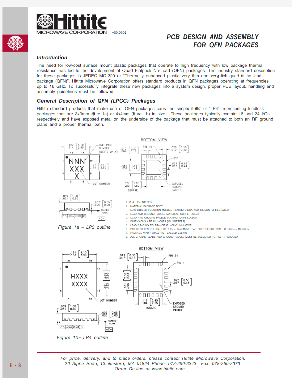
General Description of QFN (LPCC) Packages
Hittite standard products that make use of QFN packages carry the simple suffi x “LP3” or “LP4”, representing leadless packages that are 3x3mm (fi gure 1a) or 4x4mm (fi gure 1b) in size. These packages typically contain 16 and 24 I/Os respectively and have exposed metal on the underside of the package that must be attached to both an RF ground
plane and a proper thermal path.
LP3 & LP4 NOTES:
1. MATERIAL PACKAGE BODY:
LOW STRESS INJECTION MOLDED PLASTIC SILICA AND SILICON IMPREGNATED.2. LEAD AND GROUND PADDLE MATERIAL: COPPER ALLOY 3. LEAD AND GROUND PADDLE PLATING: Sn/Pb SOLDER 4. DIMENSIONS ARE IN INCHES [MILLIMETERS].
5. LEAD SPACING TOLERANCE IS NON-CUMULATIVE
6. PAD BURR LENGTH SHALL BE 0.15mm MAXIMUM. PAD BURR HEIGHT SHALL BE 0.05mm MAXIMUM.
7. PACKAGE WARP SHALL NOT EXCEED 0.05mm.
8. ALL GROUND LEADS AND GROUND PADDLE MUST BE SOLDERED TO PCB RF GROUND.
Figure 1a – LP3 outline
Figure 1b– LP4 outline
FOR QFN PACKAGES
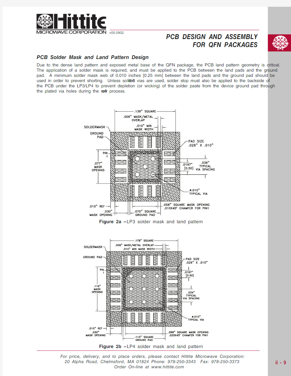
PCB Solder Mask and Land Pattern Design
Due to the dense land pattern and exposed metal base of the QFN package, the PCB land pattern geometry is critical. The application of a solder mask is required, and must be applied to the PCB between the land pads and the ground pad. A minimum solder mask web of 0.010 inches [0.25 mm] between the land pads and the ground pad should be used in order to prevent shorting. Unless solid-fi lled vias are used, solder stop must also be applied to the backside of the PCB under the LP3/LP4 to prevent depletion (or wicking) of the solder paste from the device ground pad through the plated via holes during the refl
ow process.
Figure 2a –
LP3 solder mask and land pattern
Figure 2b – LP4 solder mask and land pattern
FOR QFN PACKAGES
The land pattern and solder mask pattern for the LP3 and LP4 packages are shown with their proper alignment in fi gure 2a and 2b respectively.
Solder Paste Application
Hand soldering of LP3 and LP4 packages is not recommended due to the fi ne pitch of the package leads and the inability to properly attach the exposed metal base to the PCB. Furthermore, the use of conductive epoxy is not recommended since these epoxies will bleed, causing shorts between lands and they do not have suffi cient thermal properties. Solder paste must be used to attach QFN packages to the PCB. For proper solder thickness and alignment, the solder paste must be applied to the PCB using a stencil printer. The volume of solder paste dispensed via screen-printing will be dependent on the stencil opening and stencil thickness. A recommended stencil pattern for the LP3 and LP4 package to be used with SN63 solder paste is shown in fi gure 3a and 3b respectively. Stencil alignment to the PCB land pattern should be to within +/-1 mil to prevent formation of solder balls between the lands during the refl ow process. A PCB with properly screened solder paste is shown in Figure 4.
Component Placement
diffi cult and is not recommended. Therefore a pick-and-place machine with a microscope is recommended
for the component placement operation. Careful device placement and minimal pressure will prevent solder paste smearing. To minimize solder paste smearing, the base of the LPCC package should be brought to a height of 3-4 mils above the surface of the PCB. This will result in the LPCC package being pressed 1-2 mils into the solder paste.
Reflow Solder Process
The soldering process is usually accomplished in a refl ow oven but may also use a vapor phase process. Prior to refl owing the device, temperature profi les should be measured using the same mass as the actual assemblies. The thermocouple should be moved to various positions on the board to account for edge and corner effects and varying component masses. The fi nal profi le should be determined by mounting the thermocouple to the PCB at the location of the device. Follow solder paste and oven vendor’s recommendations when developing a solder refl ow profi le. A standard profi le will have a steady ramp up from room temperature to the pre-heat temperature to avoid damage due to thermal shock. Allow enough time between reaching pre-heat temperature and refl ow for the solvent in the paste to evaporate and the fl ux to completely activate. Refl ow must then occur prior to the fl ux being completely driven off. To help prevent the fl ux from being driven off, a steady ramp is preferred to the traditional soak. This profi le is also preferred for lead-free soldering. The duration of peak refl ow temperature should not exceed 15 seconds. QFN Packages have been qualifi ed to withstand a peak temperature of 235°C for 15 seconds. Verify that the profi le will not expose the device to temperatures in excess of 235°C. A typical refl ow profi le for the QFN package is shown in Figure 5.
Figure 3a – LP3 solder paste stencil
Figure 3b – LP4 solder paste stencil
FOR QFN PACKAGES
Figure 4 – PCB with properly screen solder paste
Reworking
In cases where the QFN package must be removed from the PCB and replaced, special tools and procedures are needed. In order to heat the QFN package suffi ciently to remove it without refl owing the solder of nearby components, a hot air workstation is recommended with an appropriate tool that limits the exposure of adjacent components to the hot air fl ow. If the part being removed will be reused, make sure not to exceed the 235°C maximum temperature of the QFN package.
Once the package has been suffi ciently heated and the solder has melted, the QFN package should be removed with tweezers. The PCB and the bottom of the QFN package must then be thoroughly cleaned and all solder and fl ux removed. Solder wick is usually suffi cient to remove the solder from the surface of the board and bottom of the QFN package.
Application of the solder paste must meet the criteria previously discussed. This can be accomplished using a solder
paste dispenser, although extreme care must be taken to apply the correct amount of paste in the proper locations. A more reliable method is to use a miniature stencil that can be applied directly onto the PCB at the location of the QFN package. Alternatively a stencil that applies the solder paste directly to the back of the QFN package can be used. Rework stencils are available from several manufacturers including the CPF (Component Print Frame) from Mini Micro Stencil Inc 1 (fi gure 6).Solder Refl ow can be accomplished using the hot-air workstation with care taken not to overheat the QFN package. Due to the small mass of the package, when the solder paste at the leads refl ows, the bottom of the package will also refl ow and the heat can then be removed.
Conclusion
The PCB layout, handling and assembly processes necessary to successfully integrate QFN packages into a system design have been detailed. These processes are easily integrated into standard PCB manufacturing lines. All of the layout and stencil drawings presented are available from the factory and can be obtained by contacting Hittite Microwave Corporation by phone or by going on-line at https://www.doczj.com/doc/d315478353.html, and completing an inquiry form.
1.
https://www.doczj.com/doc/d315478353.html,. For the LP3 package use part number CPF-16.For the LP4 package use part number CPF-24.
0501001502002500
1
2
3
45
6
7
8
LPCC Reflow Profile
T e m p e r a t u r e (C )
Time (Min.)
Figure 5 – Typical LPCC refl ow profi le
FOR QFN PACKAGES
Figure 6 – Rework
CPF stencil
QFN焊接方法 QFN封装特点 QFN是一种无引脚封装,呈正方形或矩形,封装底部中央位置有一个大面积裸露焊盘用来导热,围绕大焊盘的封装外围四周有实现电气连结的导电焊盘。由于QFN封装不像传统的SOIC 与TSOP封装那样具有鸥翼状引线,内部引脚与焊盘之间的导电路径短,自感系数以及封装体内布线电阻很低,所以它能提供卓越的电性能。此外,它还通过外露的引线框架焊盘提供了出色的散热性能,该焊盘具有直接散热通道,用于释放封装内的热量。通常将散热焊盘直接焊接在电路板上,并且PCB中的散热过孔有助于将多余的功耗扩散到铜接地板中,从而吸收多余的热量。另外相对于BGA封装,QFN封装跟方便于布线,这使得QFN封装应用越来越广泛。 下图是MPU-6050封装图 工程师在开发调试阶段,总遇到需要手工焊接QFN的时候,然而头疼的是,每次都很难焊接好,本文分享一个焊接QFN芯片的方法,需要用到的工具有: 电烙铁(此处用的是刀头的,用尖头的更好)、热烘枪,焊锡丝,细金属丝,助焊剂,酒精棉签。
QFN封装焊接方法步骤: 1.芯片引脚处理,给引脚上锡,便于后期焊接 2.焊盘表面处理,让焊盘表面平整,然后涂上助焊剂 3.将芯片对准焊盘,用热风枪加热,将芯片焊接固定在电路板上 4.用烙铁处理下四周,和短接情况,让芯片更好的和焊盘焊接在一起 5.用酒精棉签清洗芯片四周的助焊剂残渣,发现有空焊和虚焊情况
6.给芯片四周再加上助焊剂 7.取一根飞线用的细金属丝,上锡(注:若用的尖头烙铁,可以省略此步骤,直接用尖头烙铁处理空焊虚焊情况) 8.然后再让金属丝贴于芯片四周用烙铁处理芯片四周的焊盘,处理空焊虚焊情况 9.再用酒精棉签擦干净,仔细检查,观察四周引脚焊接是否光亮饱满
QF N封装芯片手工焊接方法 QFN四侧无引脚扁平封装,是一种相对比较新的IC 封装形式,QFN 外观呈正方形或矩形,大小接近于CSP,很薄很轻。元件底部具有与底面水平的焊端,在中央有一个大面积裸露焊端用来导热,围绕大面积裸露焊端的外围四周有实现电气连接的I/O 焊端,I/O 焊端有两种类型:一种只裸露出元件底部的一面,其它部分被封装在元件内;另一种焊端有裸露在元件侧面的部分。由于其尺寸小、体积小,电气性能优越,在我所得到了越来越广泛的应用。由于本人长期从事高密度印制板的组装及返修工作,对于QFN芯片的手工焊接及返修有一点实践经验,现与感兴趣的朋友分享一下。 一、焊接前准备 1、电烙铁 一般的QFN芯片都是静电敏感器件,对静电防护要求特别高,所以建议焊接前最好先对烙铁进行防静电测试,确认其符合静电防护要求。 2、加热台 我们经常用的是PACE的加热台,当然也要先确认其已经良好接地并且符合静电防护要求。 3、静电手腕 焊接前也需要用三用表确认其状态正常,并且良好接地。 4、其它常用工具 镊子、松香笔(或自制松香水)、放大镜 二、焊接步骤
1、打开电烙铁及加热台 以我常用的PACE烙铁为例,对焊端搪锡时,我一般把温度设置为260度左右,加热台视PCB材料及厚度选择合适的温度,一般为215度左右。 2、器件引脚与PCB焊盘搪锡 这一步非常重要,锡上的好不好直接关系到焊接的质量。上锡时,先要在QFN芯片的I/0焊端涂上一层助焊剂,然后将烙铁头擦拭干净,在烙铁头上沾少量锡(注意烙铁头上的锡一定不能太多,不然不同引脚间容易桥连),轻轻的沿着引脚排列方向拖一遍,这样在每一个引脚上就会形成一个漂亮的中间高四边略低的“枕形”焊点,然后对中央大面积裸露焊端搪锡,注意这里的锡不要搪的太多,不然容易因为中间锡的高度太高,使得I/O焊端焊不上,要尽量使得中央大面积裸露焊端与I/O焊端的搪锡高度大致一样。到这里对于那种只裸露出元件底部的一面,其它部分被封装在元件内的QFN 芯片来说,预加工已经完成,而对于另一种焊端有裸露在元件侧面的QFN 芯片来说还没有结束。还需要对裸露在元件侧面的引脚端面进行处理,要像给引脚搪锡一样对引脚端面进行处理,使其端面也搪上一层锡。然后用沾了酒精的擦拭纸对搪好锡的芯片进行清洗。 PCB焊盘搪锡和清洗与器件预加工方法相同。 3、器件对中 将清洗干净的芯片与PCB先各涂上一层助焊剂,然后再将芯片按资料所示方向放置在PCB上,调整芯片位置使两者精确对中。 4、焊接 用镊子轻轻的夹住己精确对中好芯片的PCB,放在温度已经升至设定温度的加热台上,用镊子轻轻的压住PCB,使其与加热台良好接触,然后注意
QFN封装 目录 概况 特点 周边引脚的焊盘设计 散热焊盘和散热过孔设计 阻焊层的考虑 1.网板设计 2.QFN焊点的检测与返修 概况 四侧无引脚扁平封装,表面贴装型封装之一。现在多称为LCC。QFN 是日本电子机械工业会规定的名称。封装四侧配置有电极触点,由于无引脚,贴装占有面积比QFP 小,高度比QFP 低。但是,当印刷基板与封装之间产生应力时,在电极接触处就不能得到缓解。因此电极触点难于作到QFP 的引脚那样多,一般从14 到100 左右。材料有陶瓷和塑料两种。当有LCC 标记时基本上都是陶瓷QFN。电极触点中心距 1.27mm。塑料QFN 是以玻璃环氧树脂印刷基板基材的一种低成本封装。电极触点中心距除1.27mm 外,还有0.65mm 和0.5mm 两种。这种封装也称为塑料LCC、PCLC、P-LCC 等。 特点 QFN是一种无引脚封装,呈正方形或矩形,封装底部中央位置有一个大面积裸露焊盘用来导热,围绕大焊盘的封装外围四周有实现电气连结的导电焊盘。由于QFN 封装不像传统的SOIC与TSOP封装那样具有鸥翼状引线,内部引脚与焊盘之间的导电
路径短,自感系数以及封装体内布线电阻很低,所以它能提供卓越的电性能。此外,它还通过外露的引线框架焊盘提供了出色的散热性能,该焊盘具有直接散热通道,用于释放封装内的热量。通常将散热焊盘直接焊接在电路板上,并且PCB中的散热过孔有助于将多余的功耗扩散到铜接地板中,从而吸收多余的热量。 图1显示了这种采用PCB焊接的外露散热焊盘的QFN封装。由于体积小、重量轻、加上杰出的电性能和热性能,这种封装特别适合任何一个对尺寸、重量和性能都有的要求的应用。我们以32引脚QFN与传统的28引脚PLCC封装相比较为例,面积(5mm×5mm)缩小了84%,厚度(0.9mm)降低了80%,重量(0.06g)减轻了95%,电子封装寄生效应也提升了50%,所以非常适合应用在手机、数码相机、PDA以及其他便携小型电子设备的高密度印刷电路板上。 图1 采用PCB焊接外露散热焊盘的QFN封装 标准或遵循工艺标准(如IPC-SM-782)来进行的。由于QFN是一个全新的封装类型,印制板焊盘设计的工业标准或指导书还没有制定出来,况且,焊盘设计完成后,还需要通过一些试验来验证。当然,在充分考虑元件底部的散热焊盘以及引脚和封装的公差等各种其他因素的情况下,仍然可以参考IPC的方法来制定设计原则。 QFN的焊盘设计主要有三个方面:①周边引脚的焊盘设计;②中间热焊盘及过孔的设计;③对PCB阻焊层结构的考虑。 周边引脚的焊盘设计 尽管在HECB设计中,引脚被拉回,对于这种封装,PCB的焊盘可采用与全引脚封装一样的设计,周边引脚的焊盘设计尺寸如图3。在图中,尺寸Zmax为焊盘引脚外侧最大尺寸,Gmin是焊盘引脚内侧最小尺寸。D2t为散热焊盘尺寸。X、Y是焊盘的宽度和长度。 图3 PCB焊盘设计尺寸