SPEC NO: DS-1085-01 FEB 02, 01
n FEATURES
l Dropout Voltage 1.3V at 3A Output Current.l Fast Transient Response.
l Extremely Tight Line and Load Regulation.l Internal Thermal and Current Limiting.
l
Adjustable Output Voltage or Fixed 1.5V, 1.8V,3.3V.
l
Standard 3-Pin Power Packages.
n APPLICATIONS
l Mother Board I/O Power Supplies.l Microprocessor Power Supplies.l High Current Regulator.
l
Post Regulator for Switching Supply.
n DESCRIPTION
The AIC1085 is a low dropout three terminal regulator with 3A output current capability. The output voltage is adjustable with the use of a resistor divider or fixed 1.5V, 1.8V, and 3.3V. Dropout is guaranteed at a maximum of 1.4V at maximum output current. Its low dropout voltage and fast transient response make it ideal for low voltage microprocessor applications. Internal current and thermal limiting provides protection against any overload condition that would create excessive junction temperatures.
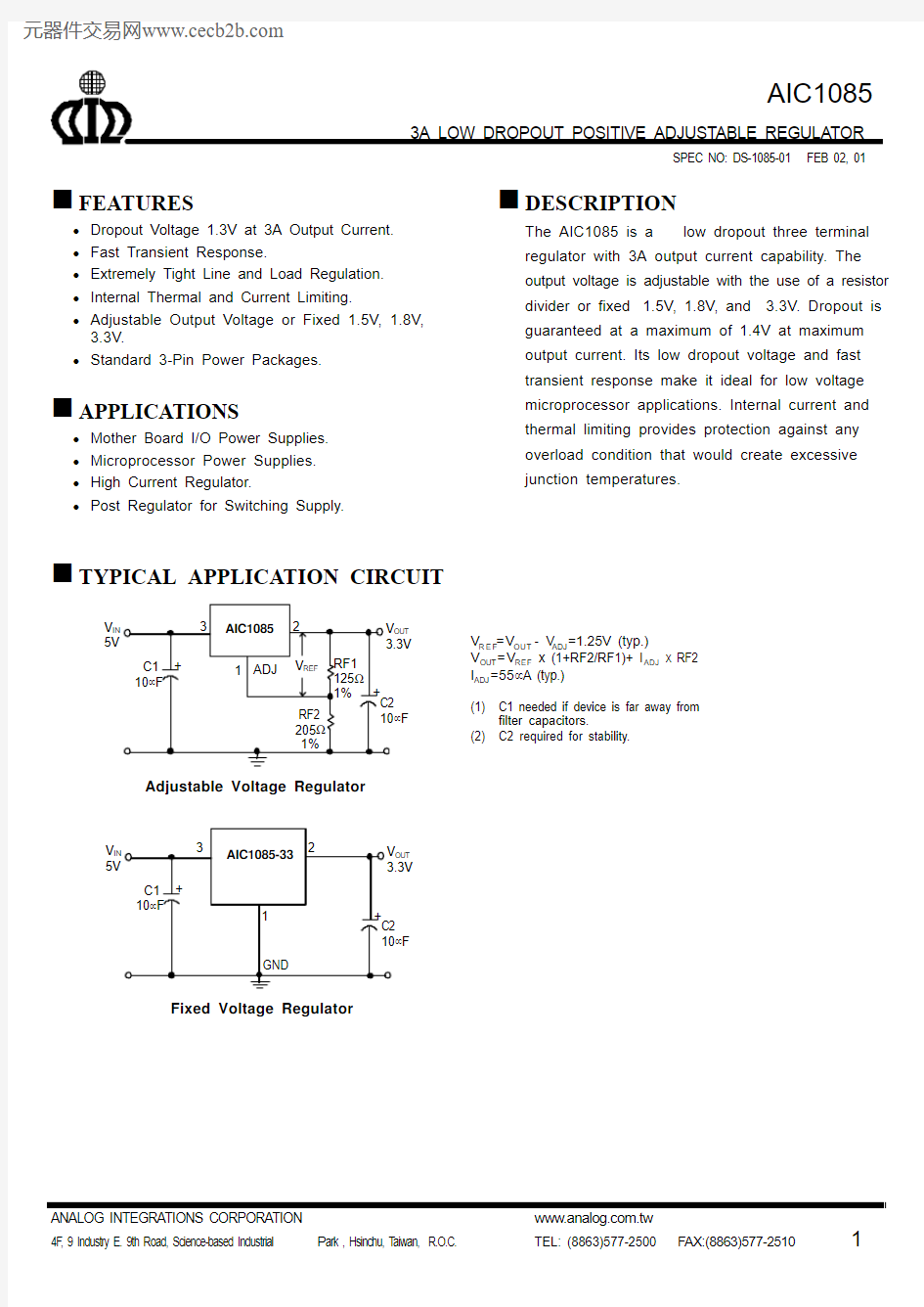
n TYPICAL APPLICATION CIRCUIT
μF OUT V IN 5V
V R E F =V OUT - V ADJ =1.25V (typ.)
V OUT =V REF x (1+RF2/RF1)+ I ADJ x RF2I ADJ =55μA (typ.)
(1) C1 needed if device is far away from
filter capacitors.
(2) C2 required for stability.
Adjustable Voltage Regulator
μF
OUT V 5V
Fixed Voltage Regulator
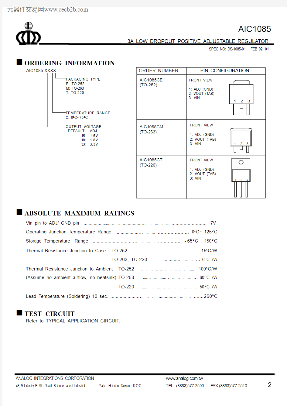
SPEC NO: DS-1085-01 FEB 02, 01 n
n ABSOLUTE MAXIMUM RATINGS
V in pin to ADJ/ GND pin .......................……...............…………….......................... 7V
O perating Junction Temperature Range..................………...................... 0°C~ 125°C
S torage Temperature Range...............................………….................-65°C ~ 150°C
T hermal Resistance Junction to Case TO-252…………………….…………… 15°C/W
TO-263, TO-220………............………... 6°C /W
T hermal Resistance Junction to Ambient TO-252…………………………..… 100°C/W
(Assume no ambient airflow, no heatsink)TO-263….....…….....……………... 60°C /W
TO-220…....……....……………….. 50°C /W
L ead Temperature (Soldering) 10 sec......................………............……..….......260°C
n TEST CIRCUIT
R efer to TYPICAL APPLICATION CIRCUIT.
SPEC NO: DS-1085-01 FEB 02, 01
n ELECTRICAL CHARACTERISTICS (V
IN
=5V, T A =25°C, I O =10mA, Unless otherwise
specified)
P ARAMETER
T EST CONDITIONS
M IN.
T YP.
M AX.
U NIT
R eference Voltage (V OUT -V ADJ ) A IC1085 (Adj.)
T A =25°C 1.238 1.25 1.262
V
O utput Voltage
A IC1085-15 V IN =5V
A IC1085-18 V IN =5V
A IC1085-33 V IN =5V 1.48 1.78 3.26 1.50 1.80
3.30 1.52 1.82 3.34 V L ine Regulation
A dj : 2.75V ≤ V IN ≤5.25V
%
F ix : V O UT +1V ≤ V IN ≤7V
T A =25°C
0.015
0.2
L oad Regulation 10mA < I O < 3A
T A =25°C 0.6
%
D ropout Voltage
?V OUT , ?V REF =1%
10mA ≤ I O ≤3A
0°C ≤T J ≤125°C 1.3 1.4
V
C urrent Limit
V IN = 5V
0°C ≤T J ≤125°C 3 4 A
A djusted Pin Current (I ADJ )
2.75V ≤ V IN ≤ 7V 55 120 μA A
djusted Pin Current Change (?I ADJ )
2.75V ≤ V IN ≤ 7V 0°C ≤T J ≤125°C
0.2
5
μA
T emperature Stability
I O =0.5A
0°C ≤T J ≤125°C 0.5 %
M inimum Load Current
0°C ≤T J ≤125°C 5 10 m A
R MS Output Noise (% of V OUT )
10Hz ≤ f ≤ 10KHz
0.003
%
R ipple Rejection Ratio
120Hz input ripple
C OUT =25μF
(V IN -V OUT )=3V 60 72
d B
SPEC NO: DS-1085-01 FEB 02, 01 n BLOCK DIAGRAM
V IN
V OUT
n PIN DESCRIPTIONS
A DJ PIN-Providing V REF=1.25V (typ.) for
adjustable V OUT. V REF=V OUT-V ADJ
and I ADJ=55μA (typ.)
(GND PIN-Power Ground.)V OUT PIN-Adjustable output voltage. V IN PIN-Power Input.
SPEC NO: DS-1085-01 FEB 02, 01
n TYPICAL PERFORMANCE CHARACTERISTICS
L o a d C u r r e n t
Time (μS)04080120160200
O u t p u t V o l t a g e (V , A C )
Line Transient Response
Time (μS)
O u t p u t V o l t a g e (m V , A C )
I n
p u t V o l t a g e (V )
010********
Dropout Voltage (VOUT=3.3V)
Output Current (A)M i n i m u m D i f f e r e n t i a l V o l t a g e (V )
0.0
0.5
1.0
1.5
2.0
2.5
3.0
1.06
1.081.101.121.141.161.181.201.22
Minimum Operating Current
Differential Voltage (V)
M i n i m u m O p e r a t i n g C u r r e n t (m A )
1
2345
0.2
0.40.60.81.01.21.41.61.8
SPEC NO: DS-1085-01 FEB 02, 01 n PHYSICAL DIMENSIONS
l TO-220 (unit: mm)
SYMBOL MIN MAX
A 3.56 4.82
D14.2316.51
E9.6610.66
e 2.29 2.79
e10.50 1.15
e2- 1.10
F0.51 1.39
J1 2.04 2.92
L12.7014.73
l TO-252 (unit: mm)
SYMBOL MIN MAX
A 2.19 2.38
A1 1.02 1.27
b0.640.88
b2 5.21 5.46
C10.460.58
D 5.33 5.59
E 6.35 6.73
e 2.28 (TYP.)
H9.4010.42
A1
L0.51-
SPEC NO: DS-1085-01 FEB 02, 01
l TO-263 (unit: mm)
SYMBOL
MIN MAX A
4.06 4.83b 0.50 1.00b2 1.14 1.40C
-0.7c2 1.14 1.40D 8.639.66E
9.6510.29e
2.54 (TYP.)
L 14.6015.88L1 2.28 2.80A
L2
-
1.40
U NIT: mm