8位超精简CPU设计参考Lattice mico8
- 格式:pdf
- 大小:572.17 KB
- 文档页数:52
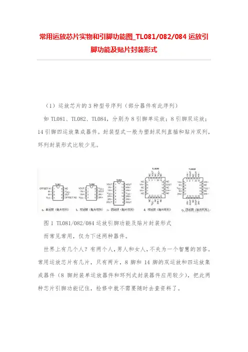
常用运放芯片实物和引脚功能图_TL081/082/084运放引脚功能及贴片封装形式(1)运放芯片的3种型号序列(部分器件有此序列)如TL081、TL082、TL084,分别为8引脚单运放;8引脚双运放;14引脚四运放集成器件。
封装型式一般为塑封双列直插和贴片双列,环列封装形式比较少见。
图1 TL081/082/084运放引脚功能及贴片封装形式而常见常用,仅为下述两种器件。
世界上有几个人?有两个人,男人和女人,不失为一个智慧的回答。
常用运放芯片有几片,只有两片,8脚和14脚的双运放和四运放集成器件(8脚封装单运放器件和环列式封装器件应用较少),把此两种芯片引脚功能记住,检修中就不需要随时去查资料了。
图2 常用运放芯片实物和引脚功能图如上图。
其封装一般为塑封双列直插DIP8/DIP14和塑封贴片工艺封装SO8/SO14两种形式,随着电子线路板小型化精密化要求的提高,贴片元件的应用占据主流,直插式器件逐渐淡出人们的视野。
但无论何种封装模式,其引脚功能、次序都是一样的,所以仅需记准8脚(双运放)和14脚(四运放)两种运放的引脚功能就够了。
(2)运放芯片的3种温度序列任何一种集成IC器件,按应用温度范围不同,都可细分为3种器件,如LM358,实际上有LM158、LM258、LM358三种型号的产品,其引脚功能、内部结构、工作原理、供电电压等等都无差别,仅仅是应用温度范围差异甚大。
LM158 适应工作温度-50℃~125℃,军工用品(1类);LM258 适应工作温度-25℃~85℃,工业用品(2类);LM358 适应工作温度0℃~70℃,农用品(3类)。
单看参数,似乎LM258适用于山东地区,若用于东北地区,其参数有些不足。
而LM358仅能适用于江南地区。
而事实上并非如此,如低于2类品规格参数被淘汰到3类品的器件,可能是-24℃~84℃温度范围以内的产品,仅次于2类品,比3类品的温度指标实际上要高许多的。
在家电元件市场能购到的多为3类品。
第1章思考题及习题参考答案1写出下列二进制数的原码、反码和补码(设字长为8位)。
(1)001011 (2)100110(3)-001011 (4)-111111答:(1)原码:00001011 反码:00001011 补码:00001011(2)原码:00100110 反码:00100110 补码:00100110(3)原码:10001011 反码:11110100 补码:11110101(4)原码:10111111 反码:11000000 补码:110000012已知X和Y,试计算下列各题的[X+Y]补和[X-Y]补(设字长为8位)。
(1) X=1011 Y=0011(2) X=1011 Y=0111(3) X=1000 Y=1100答:(1)X补码=00001011 Y补码=00000011 [–Y]补码=11111101[X+Y]补=00001110 [X-Y]补=00001000(2)X补码=00001011 Y补码=00000111 [–Y]补码=11111001[X+Y]补=00010010 [X-Y]补=00000100(3)X补码=00001000 Y补码=00001100 [–Y]补码=11110100[X+Y]补=00010100 [X-Y]补=111111003 微型计算机由那几部分构成?答:微型计算机由微处理器、存储器和I/O接口电路构成。
各部分通过地址总线(AB)、数据总线(DB)和控制总线(CB)相连。
4 8086的寻址范围有多大?其物理地址是如何形成?答:8086有20根地址总线,它可以直接寻址的存储器单元数为1M字节,其地址区域为00000H—FFFFFH。
物理地址是由段地址与偏移地址共同决定的,物理地址=段地址×16+偏移地址其中段地址通常来自于段寄存器CS ,物理地址来自于IP。
5 什么叫单片机?它有何特点?答:单片机就是在一块硅片上集成了CPU、RAM、ROM、定时器/计数器和多种I/O口(如并行、串行及A/D变换器等)的一个完整的数字处理系统。
C-SKY CK802用户手册C-SKY CK802用户手册(2014.09 Ver 1.2.8)杭州中天微系统有限公司C-SKY Microsystems Co.,Ltd声明:杭州中天微系统有限公司(C-SKY Microsystems Co.,Ltd)保留本文档的所有权利。
本文档的内容有可能发生更改、更新、删除、变动,恕不另行通知。
版权所有© 2001-2012杭州中天微系统有限公司公司地址:浙江省杭州市华星路99号东软创业大厦A403室邮政编码:310012电话:*************传真:*************-8888主页:E-mail:**************版本历史:目录:1.简介 (9)1.1.特点 (9)1.2.微体系结构 (10)1.3.编程模型 (11)1.4.数据格式 (12)1.5.指令集一览 (12)2.命名规则 (17)2.1.符号 (17)2.2.术语 (17)3.寄存器描述 (19)3.1.普通用户编程模式 (19)3.1.1.通用寄存器 (20)3.1.2.程序计数器 (20)3.1.3.条件码/进位标志位 (20)3.2.超级用户编程模式 (20)3.2.1.超级用户编程模式的堆栈指针寄存器R14(spv SP) (21)3.2.2.处理器状态寄存器(PSR,CR<0,0>) (21)3.2.3.向量基址寄存器(VBR,CR<1,0>) (23)3.2.4.异常保留寄存器(CR<2,0>~CR<5,0>) (23)3.2.5.全局控制寄存器(GCR,CR<11,0>) (23)3.2.6.全局状态寄存器(GSR,CR<12,0>) (24)3.2.7.产品序号寄存器(CPUIDRR,CR<13,0>) (24)3.2.8.高速缓存配置寄存器(CCR,CR<18,0>) (24)3.2.9.可高缓和访问权限配置寄存器(CAPR,CR<19,0>) (24)3.2.10.保护区控制寄存器(PACR,CR<20,0>) (25)3.2.11.保护区选择寄存器(PRSR,CR<21,0>) (26)3.2.12.MPU使用操作 (27)3.2.13.软件复位控制寄存器(SRCR,CR<31,0>) (27)3.2.14.普通用户模式堆栈指针寄存器14(R14(user),CR<14,1>) (27)3.3.二进制代码转译模式 (27)4.32位指令 (29)4.1.32位指令功能分类 (29)4.1.1.数据运算指令 (29)4.1.2.分支跳转指令 (31)4.1.3.内存存取指令 (31)4.1.4.特权指令 (32)4.1.5.特殊功能指令 (33)4.2.32位指令编码方式 (33)4.2.2.立即数类型 (33)4.2.3.寄存器类型 (34)4.3.32位指令操作数寻址模式 (34)4.3.1.跳转类型编码指令寻址方式 (34)4.3.2.立即数类型编码指令寻址方式 (34)4.3.3.寄存器类型编码指令寻址方式 (36)5.16位指令 (38)5.1.16位指令功能分类 (38)5.1.1.数据运算指令 (38)5.1.2.分支跳转指令 (40)5.1.3.内存存取指令 (40)5.1.4.特权指令 (41)5.2.16位指令编码方式 (41)5.2.1.跳转类型 (41)5.2.2.立即数类型 (41)5.2.3.寄存器类型 (43)5.3.16位指令操作数寻址模式 (43)5.3.1.跳转类型编码指令寻址方式 (44)5.3.2.立即数类型编码指令寻址方式 (44)5.3.3.寄存器类型编码指令寻址方式 (46)6.指令流水线 (48)7.异常处理 (51)7.1.异常处理概述 (51)7.2.异常类型 (52)7.2.1.重启异常(向量偏移0X0) (53)7.2.2.未对齐访问异常(向量偏移0X4) (53)7.2.3.访问错误异常(向量偏移0X8) (53)7.2.4.非法指令异常(向量偏移0X10) (53)7.2.5.特权违反异常(向量偏移0X14) (53)7.2.6.断点异常(向量偏移0X1C) (53)7.2.7.不可恢复错误异常(向量偏移0X20) (54)7.2.8.中断异常 (54)7.2.9.陷阱指令异常(向量偏移0X40-0X4C) (55)7.3.异常优先级 (55)7.3.1.发生待处理的异常时调试请求 (55)7.4.异常返回 (55)8.工作模式转换 (56)8.1.CK802工作模式及其转换 (56)8.1.1.正常工作模式 (56)8.1.3.调试模式 (57)附录A MPU设置示例 (58)附录B 指令术语表 (60)图表目录:图表1-1CK802结构图 (10)图表1-2编程模型 (11)图表1-3内存中的数据组织形式 (12)图表1-4寄存器中的数据组织结构 (12)图表1-5CK802的指令集 (12)图表3-1普通用户编程模式寄存器 (20)图表3-2超级用户编程模式附加资源 (21)图表3-3处理器状态寄存器 (21)图表3-4基址向量寄存器 (23)图表3-5高速缓存配置寄存器 (24)图表3-6CK802内存保护设置 (24)图表3-7可高缓和访问权限配置寄存器 (25)图表3-8访问权限设置 (25)图表3-9保护区控制寄存器 (25)图表3-10保护区大小配置和其对基址要求 (26)图表3-11保护区选择寄存器 (26)图表4-132位加减法指令列表 (29)图表4-232位逻辑操作指令列表 (29)图表4-332位移位指令列表 (30)图表4-432位比较指令列表 (30)图表4-532位数据传输指令列表 (30)图表4-632位比特操作指令列表 (30)图表4-732位提取插入指令列表 (31)图表4-832位乘除法指令列表 (31)图表4-932位杂类运算指令列表 (31)图表4-1032位分支指令列表 (31)图表4-1132位跳转指令列表 (31)图表4-1232位立即数偏移存取指令列表 (32)图表4-1432位多寄存器存取指令列表 (32)图表4-1532位控制寄存器操作指令列表 (32)图表4-1632位低功耗指令列表 (32)图表4-1732位异常返回指令列表 (32)图表4-1832位特殊功能指令列表 (33)图表5-116位加减法指令列表 (38)图表5-216位逻辑操作指令列表 (38)图表5-316位移位指令列表 (39)图表5-416位比较指令列表 (39)图表5-516位数据传输指令列表 (39)图表5-616位比特操作指令列表 (39)图表5-716位提取插入指令列表 (39)图表5-816位乘法指令列表 (40)图表5-916位分支指令列表 (40)图表5-1016位跳转指令列表 (40)图表5-1116位立即数偏移存取指令列表 (40)图表5-1216位多寄存器存取指令列表 (40)图表5-1316位二进制转译堆栈指令 (41)图表4-1816位特殊功能指令列表 (41)图表6-1各级流水线作用 (48)图表6-2单周期指令流水线重叠执行 (48)图表6-3乘法指令MULT的执行过程 (48)图表6-4BR,BSR指令的跳转和条件指令预测正确时的执行过程 (49)图表6-5JMP指令执行过程 (49)图表6-6跳转指令的目标指令是32位字未对齐指令的执行过程 (49)图表6-7带有等待状态的指令流水执行过程 (50)图表6-8具有快速退休功能的指令流水执行过程 (50)图表7-1异常向量分配 (52)图表7-3中断处理过程 (54)图表7-4异常优先级 (55)图表10-1CPU的各种工作状态示意图 (56)1. 简介CK802是杭州中天微系统有限公司自主研发的极低功耗、极低成本嵌入式CPU核,以8位CPU的成本获得32位嵌入式CPU的运行效率与性能。

MIPS芯片架构说明MIPS(Microprocessor without Interlocked Pipeline Stages)即无竞争流水线微处理器,是一种精简指令集(RISC)的芯片架构。
MIPS 架构由美国斯坦福大学的约翰·亨尼西等人于1981年提出,并于1984年成立MIPS公司进行商业化开发和推广。
MIPS架构在计算机领域有着广泛的应用,尤其在网络设备、数字视频处理、嵌入式系统等领域具有重要地位。
MIPS架构的设计理念是简化指令集,提高流水线效率,以提供高性能和高效能的微处理器。
MIPS指令集体系结构的特征包括:固定长度的32位指令;寄存器-寻址模式;延迟槽;无跳转偏移;定长延迟分支;乱序执行指令流水线;五级流水线等。
MIPS指令集是一种精简的指令集,通过减少指令种类、规定固定的指令格式和长度,以及简化指令的操作模式,达到提高指令执行效率的目的。
MIPS指令集包括加载存储指令,算术逻辑运算指令,分支和跳转指令,协处理器指令等。
MIPS架构采用寄存器-寻址模式来访问数据。
寄存器-寻址模式是指通过指定寄存器的编号来操作数据,而不是通过指定内存地址。
MIPS架构提供了32个通用寄存器,用于存储数据和中间结果,通过对寄存器的操作来实现数据的传输和计算。
这种设计简化了指令的编码和执行,提高了指令执行的效率。
MIPS架构中的延迟槽是指在条件分支指令后的一条或多条指令,不管条件是否满足都会执行。
延迟槽的设计可以充分利用流水线的性能,但需要程序员进行特殊的处理,以确保延迟槽的指令在分支满足或不满足时都能正确执行。
MIPS架构的指令集中,分支和跳转指令的目标地址是相对于当前指令的偏移地址。
相对地址的设计简化了指令的编码和目标地址的计算,提高了指令的执行效率。
MIPS架构中的乱序执行指令流水线是指将多条指令按照最大并行度进行重排序,在这个过程中可能会引入数据依赖、资源竞争等问题。
为了解决这些问题,MIPS架构采取了一系列的措施,如指令重排序、数据前推、动态分支预测等,以提高指令的并行度和流水线的效率。

MIPS CPU详细介绍MIPS是世界上很流行的一种RISC处理器。
MIPS的意思是“无内部互锁流水级的微处理器”(Microprocessor without interlocked piped stages),其机制是尽量利用软件办法避免流水线中的数据相关问题。
它最早是在80年代初期由斯坦福(Stanford)大学Hennessy教授领导的研究小组研制出来的。
MIPS公司的R系列就是在此基础上开发的RISC工业产品的微处理器。
这些系列产品为很多计算机公司采用构成各种工作站和计算机系统。
MIPS技术公司是美国著名的芯片设计公司,它采用精简指令系统计算结构(RISC)来设计芯片。
和英特尔采用的复杂指令系统计算结构(CISC)相比, RISC 具有设计更简单、设计周期更短等优点,并可以应用更多先进的技术,开发更快的下一代处理器。
MIPS是出现最早的商业RISC架构芯片之一,新的架构集成了所有原来MIPS指令集,并增加了许多更强大的功能。
1986年推出R2000处理器,1988年推出R3000处理器,1991年推出第一款64位商用微处理器R4000。
之后,又陆续推出R8000(于 1994年)、R10000(于1996年)和R12000(于1997年)等型号。
1999年,MIPS公司发布MIPS 32和MIPS 64架构标准。
2000年,MIPS公司发布了针对MIPS 32 4Kc的新版本以及未来64位MIPS 64 20Kc处理器内核。
在MIPS芯片的发展过程中,SGI公司在1992年收购了MIPS计算机公司,1998年,MIPS公司又脱离了SGI,成为MIPS技术公司; MIPS32 4KcTM 处理器是采用MIPS技术特定为片上系统(System-On-a-Chip)而设计的高性能、低电压32位MIPS RISC 内核。
采用MIPS32TM体系结构,并且具有R4000存储器管理单元(MMU)以及扩展的优先级模式,使得这个处理器与目前嵌入式领域广泛应用的 R3000和R4000系列(32位)微处理器完全兼容.新的 64 位 MIPS 处理器是RM9000x2,从“x2”这个标记判断,它包含了不是一个而是两个均具有集成二级高速缓存的64位处理器。
TOTAL:2DRAWING (1)SPOT Ag THICKNESS [局部D.Ag 厚度]:3.0~8.0μm AMF'7.323.A.2C36MM PLATING UNITMATERIAL[材料]:A194-F.H.NINGBO KANGQIANG ELECTRONICS CO.,LTDTHE NO: 1SOP8L-A8(60×60)LEADFRAME [引线框架]SIGNER DATE REV NO.QTY DRAWN BY PROCESS CHK'D BY APPROVED BY STANDARD A M F '7.323.A .2C NOTE[技术要求]:1.DIMENSION QUADRANT IS SYMMETRICAL FOR ALL QUADRANTS EXCEPT OTHERWISE SHOWN. [除另有说明,所有象限的尺寸都是对称的。
]2.GENERAL TOLERANCE UNLESS OTHER SPECIFIED:±0.050. [未注尺寸公差为±0.050]3.RADIUS UNLESS OTHER SPECIFIED[未注圆角半径]: R0.127 MAX 4.VERTICAL BURR[垂直毛刺]: 0.025 MAX HORIZONTAL BURR[水平毛刺]: 0.051 MAX 5.MINIMUM LEAD SPACE[最小引线脚间隙]:0.10 MIN 6.LEAD TIP PLANARITY FROM DAM BAR [从中筋到引线内脚的平面度]:±0.1027.PAD FLATNESS[基岛平面度]:0.010/2.540 MAX 8.LEAD TIP FLAT WIDTH[引线内脚平面的宽度]:0.225 MIN 9.CAMBER[侧弯]:0.041 MAX ; COIL SET[卷弯]: 0.508 MAX CROSS BOW[横弯]: 0.254 MAX 10.PAD TILT[基岛倾斜]:0.051/2.540 MAX 11.PAD PLANARITY[基岛平面公差]:±0.10212.COINING DEPTH[精压深度]:0.038 MAX 13.LEAD TWIST[引线脚扭曲]:2.5°MAX 14.FRAME TWIST[引线框扭曲]:0.508 MAX 15.LEAD TILT[引线脚倾斜]:2.5°MAX 16.THE FOURTH DECIMAL PLACE IS USED FOR TOOLING REFERENCE ONLY.[第四位小数仅被用于开引线框架模具时参考的]17.PART TO BE FREE OF RUST,KINKS,BENDS,WRINKLES,SLUG OR TOOL MARKS,OR SCRATCHES DEEPER THAN 0.007. EXT LEAD SPANKING MARK IS IMPOSED 0.254 AWAY FROM DAM BAR. [产品铁锈、 纽绞、弯曲、皱纹、断裂或模具压痕或刮伤程度不超过0.007mm]18.SPOT SILVER,SEMI-BRIGHT.[局部点状镀银,半光亮]19.DIMENSIONS SHOWN FOR INTERNAL LEAD POSITIONS REPRESENT THAT AFTER STAMPING BUT BEFORE COINING [已标出的引线内脚位置的尺寸是冲压之后精压之前的尺寸]20.D/S TOOL MARK ON TIE BAR ONLY,WITH DEPTH [打弯压印,深度]≤0.05121.PLATING AREA[镀银区域]: MIN[最小]2.80×2.70 MAX[最大]3.30×3.1022.DIE PAD SIZE[装片区尺寸]: 1.524×1.524 (60×60)67.000065.600064.000063.000058.150055.000050.150049.625047.525047.000042.150039.000034.150031.000026.150025.625023.525023.000018.150015.000010.15007.0000 2.15001.40001.15000.0000 5.05000.00005.47505.98308.30009.350010.400014.900020.375020.883024.25001.5240±0.0250.40000.4000±0.0251.2700±0.02530°68.500065.400061.500057.600057.200055.885053.500049.400047.325045.500037.500029.500023.325021.500013.5000 5.5000 1.60000.61708.0000±0.0253.18001.90007.600011.720016.800022.5000R0.25001.5240Ø1.5240±0.025Ø1.000025.825049.825057.40005.35004.07001.27505.0750KQ 11ED100601马叶军2010-6-2TOTAL:2DRAWING (1)SPOT Ag THICKNESS [局部D.Ag 厚度]:3.0~8.0μm AMF'7.323.A.2C36MM UNITMATERIAL[材料]:A194-F.H.NINGBO KANGQIANG ELECTRONICS CO.,LTDTHE NO: 2SOP8L-A8(60×60)LEADFRAME [引线框架]SIGNER DATE REV NO.QTY DRAWN BY PROCESS CHK'D BY APPROVED BY STANDARD A M F '7.323.A .2C 70.0000±0.051256 PAD / STRIP 29.8000±0.02514.9000±0.0255.3500±0.0769.1500±0.07615*14.9±0.025=223.5000±0.051238.0000±0.102 3.17502.82751.6500 MAX PLATING 1.4000 MIN PLATING & COIN 0.00000.76202.52752.79503.22502.35002.4500 PKG.0.90000.15001.00001.5050 2.1350 1.45001.25000.96500.17700.12700.2500 1.5335 2.13501.9500 PKG.1.5500 MAX PLATING 1.3500 MIN PLATING & COIN 0.74000.42000.20000.00000.7620 1.60004.0000±0.102R0.150045°BURR SIDE [毛刺面]PLATING SIDE [电镀面]45°A A A-A 0.2030±0.0080.1650±0.0250.3450 MIN COIN 0.3100 MIN COINB B B-B 50:10.010~0.03860° 2.4500BURR SIDE [毛刺面] 1.00000.2500 1.9350KQ 11ED100601马叶军2010-6-2TOTAL:2DRAWING (1)SPOT Ag THICKNESS [局部D.Ag 厚度]:3.0~8.0μm AMF'7.323.A.2C45MM PLATING UNITMATERIAL[材料]:A194-F.H.NINGBO KANGQIANG ELECTRONICS CO.,LTDTHE NO: 1SOP8L-B8(130×95)LEADFRAME [引线框架]SIGNER DATE REV NO.QTY DRAWN BY PROCESS CHK'D BY APPROVED BY STANDARD A M F '7.323.A .2C NOTE[技术要求]:1.DIMENSION QUADRANT IS SYMMETRICAL FOR ALL QUADRANTS EXCEPT OTHERWISE SHOWN. [除另有说明,所有象限的尺寸都是对称的。
LatticeMico8 Processor Reference ManualDecember 2012CopyrightCopyright © 2012 Lattice Semiconductor Corporation.This document may not, in whole or part, be copied, photocopied, reproduced, translated, or reduced to any electronic medium or machine-readable form without prior written consent from Lattice Semiconductor Corporation.TrademarksLattice Semiconductor Corporation, L Lattice Semiconductor Corporation (logo), L (stylized), L (design), Lattice (design), LSC, CleanClock, Custom Movile Device, DiePlus, E2CMOS, Extreme Performance, FlashBAK, FlexiClock, flexiFLASH, flexiMAC, flexiPCS, FreedomChip, GAL, GDX, Generic Array Logic, HDL Explorer, iCE Dice, iCE40, iCE65, iCEblink, iCEcable, iCEchip, iCEcube, iCEcube2, iCEman, iCEprog, iCEsab, iCEsocket, IPexpress, ISP, ispATE, ispClock, ispDOWNLOAD, ispGAL, ispGDS, ispGDX, ispGDX2, ispGDXV, ispGENERATOR, ispJTAG, ispLEVER, ispLeverCORE, ispLSI, ispMACH, ispPAC, ispTRACY, ispTURBO, ispVIRTUAL MACHINE, ispVM, ispXP, ispXPGA, ispXPLD, Lattice Diamond, LatticeCORE, LatticeEC, LatticeECP, LatticeECP-DSP, LatticeECP2, LatticeECP2M, LatticeECP3, LatticeECP4, LatticeMico, LatticeMico8, LatticeMico32, LatticeSC, LatticeSCM, LatticeXP, LatticeXP2, MACH, MachXO, MachXO2, MACO, mobileFPGA, ORCA, PAC, PAC-Designer, PAL, Performance Analyst, Platform Manager, ProcessorPM, PURESPEED, Reveal, SiliconBlue, Silicon Forest, Speedlocked, Speed Locking, SuperBIG, SuperCOOL, SuperFAST, SuperWIDE, sysCLOCK, sysCONFIG, sysDSP, sysHSI, sysI/O, sysMEM, The Simple Machine for Complex Design, TraceID, TransFR, UltraMOS, and specific product designations are either registered trademarks or trademarks of Lattice Semiconductor Corporation or its subsidiaries in the United States and/or other countries. ISP, Bringing the Best Together, and More of the Best are service marks of Lattice Semiconductor Corporation.Other product names used in this publication are for identification purposes only and may be trademarks of their respective companies.DisclaimersNO WARRANTIES: THE INFORMATION PROVIDED IN THIS DOCUMENT IS “AS IS” WITHOUT ANY EXPRESS OR IMPLIED WARRANTY OF ANY KIND INCLUDING WARRANTIES OF ACCURACY, COMPLETENESS, MERCHANTABILITY, NONINFRINGEMENT OF INTELLECTUAL PROPERTY, OR FITNESS FOR ANY PARTICULAR PURPOSE. IN NO EVENT WILL LATTICE SEMICONDUCTOR CORPORATION (LSC) OR ITS SUPPLIERS BE LIABLE FOR ANY DAMAGES WHATSOEVER (WHETHER DIRECT, INDIRECT, SPECIAL, INCIDENTAL, OR CONSEQUENTIAL, INCLUDING, WITHOUT LIMITATION, DAMAGES FOR LOSS OF PROFITS, BUSINESS INTERRUPTION, OR LOSS OF INFORMATION) ARISING OUT OF THE USE OF OR INABILITY TO USE THE INFORMATION PROVIDED IN THIS DOCUMENT, EVEN IF LSC HAS BEEN ADVISED OF THE POSSIBILITY OF SUCH DAMAGES. BECAUSE SOME JURISDICTIONS PROHIBIT THE EXCLUSION OR LIMITATION OF CERTAIN LIABILITY, SOME OF THE ABOVE LIMITATIONS MAY NOT APPLY TO YOU.LSC may make changes to these materials, specifications, or information, or to the products described herein, at any time without notice. LSC makes no commitment to update this documentation. LSC reserves the right to discontinue any product or service without notice and assumes no obligation to correct any errors contained herein or to advise any user of this document of any correction if such be made. LSC recommends its customers obtain the latest version of the relevant information to establish, before ordering, that the information being relied upon is current.Type Conventions Used in This DocumentConvention Meaning or UseBold Items in the user interface that you select or click. Text that you type into the user interface.<Italic>Variables in commands, code syntax, and path names.Ctrl+L Press the two keys at the same time.Courier Code examples. Messages, reports, and prompts from the software. ...Omitted material in a line of code.Omitted lines in code and report examples....[ ]Optional items in syntax descriptions. In bus specifications, the brackets are required.( )Grouped items in syntax descriptions.{ }Repeatable items in syntax descriptions.| A choice between items in syntax descriptions.ContentsIntroduction 1Architecture 3Register Architecture3General-Purpose Registers3Control and Status Registers4 Memory Architecture5Memory Regions5Memory Modes9Interrupt Architecture10Call Stack10Configuration Options 11Instruction Set 13Instruction Formats13Instruction Set Lookup Table14 Instruction Descriptions16Programming Model 37Data Representation37Procedure Caller-Callee Convention38 Register Usage38Stack Frame39Parameter Passing40Interrupt Convention41Acessing LatticeMico8 Memory Regions42 Scratchpad42Peripheral42PROM43C ONTENTSIndex 45Chapter 1 IntroductionThe LatticeMico8™ is an 8-bit microcontroller optimized for Field Programmable Gate Arrays (FPGAs) and Programmable Logic Device architectures from Lattice Semiconductor. It combines a full 18-bit wide instruction set with 16 or 32 general-purpose registers. It is suitable for a wide variety of markets, including communications, consumer, computer, medical, industrial and automotive. The core consumes minimal device resources— fewer than 250 Look-Up Tables (LUTs) in the smallest configuration—while maintaining a broad feature set.LatticeMico8 Features◆8-Bit Data Path◆18-Bit Instructions◆Configurable Instruction Memory (PROM)◆Internal, or external through the WISHBONE Interface◆Configurable to accommodate 256, 512, 1K, 1.5K, 2K, 2.5K, 3K, 3.5Kor 4K instructions◆Scratchpad Memory◆Internal, or external through the WISHBONE Interface◆Configurable up to 4Gbytes using paged bytes (256 bytes/page)◆Input/Output Peripheral Space through the WISHBONE Interface◆Configurable up to 4Gbytes using paged ports (256 ports/page)◆Minimum Two Cycles per Instruction◆Configurable 16 or 32 General-purpose Registers◆Configurable Call Stack sizeFigure1 on page2 shows the LatticeMico8 Microcontroller block diagram.I NTRODUCTION:Figure 1: LatticeMico8 Microcontroller CoreChapter 2ArchitectureThis chapter describes the LatticeMico8 register and memory architectureand explains the interrupt architecture and call stack.Register ArchitectureThis section describes the general-purpose and control and status registers ofthe LatticeMico8 architecture.General-Purpose RegistersThe LatticeMico8 microcontroller can be configured to have either 16 or 32general-purpose registers. Each register is 8 bits wide. The registers areimplemented using a dual-port distributed memory. The LatticeMico8 opcodeset permits the microcontroller to access 32 registers. When LatticeMico8 isconfigured with 16 registers, any opcode reference to R16 to R31 maps to R0to R15 respectively.General-purpose registers R13, R14, and R15 can also be used by theLatticeMico8 microcontroller as page-pointer registers, depending on thecurrent memory mode. Page pointers (PP) are used when the scratchpad andperipheral memory spaces are larger than 256 bytes (see “Memory Modes”on page9). The memory address is formed by concatenating the values inregisters R13, R14, and R15 with an 8-bit value derived from the LatticeMico8memory instruction. Table1 on page4 highlights the three LatticeMico8memory modes and corresponding designation of registers R13, R14, andR15.In the large memory mode, registers R13, R14, and R15 indicate which ofthe 16M pages is currently active. R13 provides the least-significant byteof page address and R15 provides most-significant byte.A RCHITECTURE :Register ArchitectureIn the medium memory mode, register R13 indicates which of the 256pages is currently active.Control and Status RegistersTable 2 shows all the names of the control and status registers (CSR), theread and write access, and the index used when the register is accessed. Allsignal levels are active high.IP – Interrupt Pending The IP CSR contains a pending bit for each of the 8external interrupts. A pending bit is set when the corresponding interruptrequest line is asserted low. Bit 0 corresponds to interrupt 0. Bits in the IPCSR can be cleared by writing a 1 with the wcsr instruction. Writing a 0 has noeffect. After reset, the value of the IP CSR is 0.IM – Interrupt Mask The IM CSR contains an enable bit for each of the 8external interrupts. Bit 0 corresponds to interrupt 0. In order for an interrupt tobe raised, both an enable bit in this register and the IE flag in the IE CSR mustbe set to 1. After reset, the value of the IM CSR is 0.IE – Global Interrupt Enable The IE CSR contains a single-bit (bit position0) flag, IE, which determines whether interrupts are enabled. This flag haspriority over the IM CSR. After reset, the value of the IE CSR is 0.Table 1: Designation of LatticeMico8 Registers Based on LatticeMico8 Memory ModeRegister NumberLatticeMico8 Memory ModeSmall Medium Large 0 through 12general-purpose general-purpose general-purpose 13general-purpose PP PP (LSB)14general-purpose general-purpose PP 15general-purpose general-purpose PP (MSB)16 through 31general-purpose general-purpose general-purposeTable 2: Control and Status RegistersNameAccess Index Description IPR/W 0Interrupt Pending IMR/W 1Interrupt Mask IE R/W 2Global Interrupt Enable/DisableA RCHITECTURE:Memory ArchitectureMemory ArchitectureThis section describes the memory architecture of the LatticeMico8microcontroller.Memory RegionsThe LatticeMico8 microcontroller recognizes three independent memoryregions. Each memory region has its own independent input/output interfaceand its own instruction set support. These three memory regions are calledthe PROM, the Scratchpad, and the Peripheral memory regions respectively.The size and location of each of these memory regions is configurable as longas all these three memory regions are located entirely within the 4GB addressspace. These memory regions can also be configured to overlap withinLatticeMico System Builder. Figure2 shows the three memory regions andthe address space to which they are confined by LatticeMico System Builder.See “Acessing LatticeMico8 Memory Regions” on page42 for details on howto access each of the three memory regions from a software programmer'sperspective.Figure 2: Memory OrganizationA RCHITECTURE:Memory ArchitecturePROM SpaceThe PROM memory region contains the program code that will be executedby the LatticeMico8 microcontroller core and is accessible via its instructionfetch engine. The size of the PROM memory region can be configured toaccommodate 256, 512, 1024, 2048, or 4096 instruction opcodes. By defaultthe memory region is located within the LatticeMico8 microcontroller. Thememory regions can also be configured to be external to the LatticeMico8microcontroller.When the PROM memory region is internal to the microcontroller, it isconnected to the LatticeMico8 instruction fetch engine via a dedicated high-speed bus that fetches one instruction opcode per clock cycle. There is noinstruction set support to write to internal PROM. When the PROM memoryregion is external to the microcontroller, it is accessed by the masterWISHBONE interface within the LatticeMico8 instruction fetch engine. ThisWISHBONE interface has a 8-bit data bus and it takes three 8-bit WISHBONEaccesses to fetch one LatticeMico8 instruction opcode. The instruction fetchlatency is now dictated by the system WISHBONE latency and the latency ofthe PROM memory. The minimum instruction fetch latency is 12 clock cycles.Table3 shows the WISHBONE interface signals. For more information aboutthe WISHBONE System-On-Chip (SoC) Interconnection Architecture forPortable IP Cores, as it is formally known, refer to the Web site at /projects.cgi/web/wishbone.Table 3: PROM WISHBONE Interface SignalsName Width Direction DescriptionI_CYC_O1Output A new LatticeMico8 instruction fetch request is initiated by asserting thissignal. This signal remains asserted until I_ACK_I is asserted, whichindicates the completion of the request.I_STB_O1Output A new LatticeMico8 instruction fetch request is initiated by asserting thissignal. This signal may be valid only for the first cycle.I_CTI_O2Output Always has a value 2’b00I_BTE_O3Output Always has a value 3’b000I_ADR_O32Output The address output array I_ADR_O( ) is used to pass a binary address.I_WE_O1Output Always has a value 1’b0I_SEL_O4Output Always has a value 4’b1111I_DAT_O8Output UnusedI_LOCK_O1Output Unused (signal exists, but it is not implemented)I_ACK_I1Input When asserted, the signal indicates the normal termination of a bus cycleand that an instruction is available on I_DAT_I bus.I_ERR_I1Input Unused (signal exists, but it is not implemented)I_RTY_I1Input Unused (signal exists, but it is not implemented)I_DAT_I8Input One byte of the LatticeMico8 18-bit instruction opcode is available on thisbus when I_ACK_I is asserted. It takes three WISHBONE transactions tocomplete one LatticeMico8 instruction fetch.A RCHITECTURE :Memory ArchitectureThe advantage of configuring the PROM memory region as external to the LatticeMico8 microcontroller is that the PROM memory region can now be configured to overlap with other LatticeMico8 memory regions within Lattice Mico System Builder and, therefore, be directly written to by LatticeMico8 opcodes. This configuration also offers the ability to store and executeLatticeMico8 instructions from non-volatile memory such as Flash. As shown in Figure 2 on page 5, the external PROM memory region can be placed at any location within a 4GB address range. When the LatticeMico8microcontroller is instantiated using Lattice Mico System Builder, it will restrict the placement of external PROM between 0x00000000 and 0x80000000.Scratchpad SpaceLatticeMico8 provides an independent memory space that is designed to be used for program read/write and read-only data as well as other user-defined data. The size of this scratchpad memory can be configured from 32 bytes to 4G bytes, in power-of-two increments. Figure 3 shows the structure of this scratchpad space and how data is located within this space. The scratchpad memory space can be placed at any location within a 4GB address range. The first 4 bytes are reserved for LatticeMico8 interrupt handling. Program data is situated above this reserved space. The designer can configure the size of scratchpad memory that is used for program data. User-defined data is optional and is always located after program data.The scratchpad memory can be configured to be entirely internal to theLatticeMico8 microcontroller, entirely external to LatticeMico8 microcontroller, or a combination of both.◆The internal scratchpad is implemented using single-port EBRs and is hooked up to the LatticeMico8 core through a dedicated bus. Reads or writes to the internal scratchpad take a single clock cycle.◆The external scratchpad is accessed through the Peripheral WISHONE interface of the LatticeMico8 microcontroller (see “Interrupt Architecture” on page 10). Each read or write will take a minimum of 2 clock cycles.Figure 3: Scratchpad Space StructureA RCHITECTURE:Memory ArchitecturePeripheral (Input/Output) SpaceLatticeMico8 provides an independent memory space that is designed to beused for peripherals and other memory-mapped hardware. The size of thisperipheral memory space can be configured from 0 bytes to 4G bytes inpower-of-two increments. While the peripheral memory space can be placedat any location within a 4GB address range, Lattice Mico System Builderrestricts the peripheral memory space to the addresses between 0x80000000and 0xFFFFFFFF.This memory space is always external to the LatticeMico8 microcontroller andis primarily used to enable LatticeMico8 to communicate with memory-mapped hardware and peripherals. The LatticeMico8 microcontroller cancommunicate with any hardware or peripheral within the peripheral memoryspace, through the peripheral WISHBONE interface within LatticeMico8 core,using LatticeMico8 instruction opcodes. This WISHBONE interface has 8-bitinput and output data busses and a 32-bit address bus. Table4 shows thePeripheral WISHBONE interface signals.Table 4: Peripheral WISHBONE Interface SignalsName Width Direction DescriptionD_CYC_O1Output A new LatticeMico8 data request is initiated by asserting this signal.This signal remains asserted until D_ACK_I is asserted, whichindicates completion of the request.D_STB_O1Output A new LatticeMico8 data request is initiated by asserting this signal.This signal may be valid only for first cycle.D_CTI_O2Output This bus will always have a value 2'b00D_BTE_O3Output This bus will always have a value 3'b000D_ADR_O32Output The address output array D_ADR_O( ) is used to pass a binaryaddress. D_ADR_O( ) actually has a full 32 bits.D_WE_O1Output This signal indicates whether a new data request is a read (0) or awrite (1). This signal must hold its value as long as D_CYC_O isasserted.D_SEL_O1Output Always has a value 1'b1D_DAT_O8Output Has valid data when D_WE_O is 1'b1.D_LOCK_O1Output Unused (signal exists, but it is not implemented)D_ACK_I1Input When asserted, the signal indicates the normal termination of a buscycle.D_ERR_I1Input Unused (signal exists, but it is not implemented)D_RTY_I1Input Unused (signal exists, but it is not implemented)D_DAT_I8Input Data is available on this bus when D_ACK_I and D_WEO areasserted.A RCHITECTURE:Memory ArchitectureMemory ModesThe LatticeMico8 microcontroller can be configured for different sizes for thescratchpad and peripheral memory regions. The size of scratchpad andperipheral memory regions can be as small as 32 bytes and as large as 4Gbytes. A 32-byte memory region requires only 5 address bits, while a 4GBmemory region requires 32 address bits.The LatticeMico8 instruction set can directly access only 256 memorylocations, since all general-purpose registers are 8 bits wide. (See “InstructionSet” on page13.) To access memory regions that are larger than 256 bytes,LatticeMico8 relies on a concept called “paging,” in which the memory islogically divided into 256-byte pages. The memory address is composed oftwo parts, as shown in Figure4: the page index and the page pointer. Thepage index is 8 bits wide and addresses a byte in the currently active page,while the page pointer provides the address of the currently active page. Figure 4: Memory ModesThe page pointers are essentially general-purpose registers that have beenretargeted to provide a memory address. (See “Memory Regions” on page5.)Table5 shows the memory modes of the LatticeMico8 microcontroller, thesize of addressable memory space in each mode, and the general-purposeregisters used as page pointers.Table 5: LatticeMico8 Memory ModesMemory Mode Maximum Memory Size Address Bits Page Pointer RegistersSmall256 bytes8N/AMedium16K bytes16R13Large4G bytes32R13, R14, R15A RCHITECTURE:Interrupt ArchitectureInterrupt ArchitectureThe LatticeMico8 microcontroller supports up to 8 maskable, active-low, level-sensitive interrupts. Each interrupt line has a corresponding mask bit in the IMCSR. The mask enable is active high. A global interrupt-enable flag isimplemented in the IE CSR. The software can query the status of theinterrupts and acknowledge them through the IP CSR. If more interruptsources or more sophisticated interrupt detection methods are required,external interrupt controllers can be cascaded onto the microcontroller’sinterrupt pins to provide the needed functionality.When an interrupt is received, the address of the next instruction is pushedinto the call stack (see “Call Stack” on page10), and the microcontrollercontinues execution from the interrupt vector (address 0). The flags (carry andzero) are pushed onto the call stack along with the return address. An iretinstruction will pop the call stack and transfer control to the address on top ofthe stack. The flags (carry and zero) are also popped from the call stack.See “Interrupt Convention” on page41 for details on the programming modelfor interrupts.NoteThe LatticeMico8 microcontroller does not support nested interrupts. Locations 0through 3 in the scratchpad are reserved for interrupt handling and should not used forany other purpose.Call StackThe LatticeMico8 microcontroller implements a hardware call stack to handleprocedure calls (call instruction) and procedure/interrupt return (ret and iretinstructions). The depth of this call stack determines the number of nestedprocedure calls that can be handled by the LatticeMico8 microcontroller, anddesigners can choose the depth to be 8, 16, or 32. When a call instruction isexecuted, the address of the next instruction is pushed on to the call stack. Aret or iret instruction will pop the stack and continue execution from thelocation at the top of the stack.NoteThere is no mechanism in hardware to detect whether the number of nested procedurecalls has exceeded the depth of the call stack. It is up to the software developer toensure that the call stack does not overflow.Chapter 3Configuration OptionsThe LatticeMico8 microcontroller is reconfigurable. Table6 outlines thevarious configuration options that are available to a designer.Table 6: LatticeMico8 Configuration OptionsParameter Name DescriptionLATTICE_FAMILY The target Lattice FPGA family.CFG_PROM_INIT_FILE Provides the file that contains the initialization data (program code) for aninternal PROM.CFG_PROM_INIT_FILE_FORMAT Indicates whether CFG_PROM_INIT_FILE is in hex (default) or binary. CFG_PROM_SIZE Indicates the number of instructions that can be accommodated in thePROM.CFG_SP_INIT_FILE Provides the file that contains the initialization data (program data) for aninternal scratchpad.CFG_SP_INIT_FILE_FORMAT Indicates whether CFG_SP_INIT_FILE_FORMAT is hex (default) or binary. SP_PORT_ENABLE Indicates whether the scratchpad is internal (value 1) or external (value 0).The default is 1.SP_SIZE Indicates the number of bytes in the scratchpad.SP_BASE_ADDRESS Provides the base address of the scratchpad, regardless of whether it isinternal or external.CFG_IO_BASE_ADDRESS Provides the base address of the peripheral memory region.CFG_EXT_SIZE_[8|16|32]Indicates the size of address bus for the scratchpad and peripheral memoryregions and, therefore, identifies the LatticeMico8 memory mode. Thedefault is 16 (medium memory mode).CFG_REGISTER_[16|32]Indicates the number of general-purpose registers in LatticeMico8. Thedefault is 8.C ONFIGURATION O PTIONS:Table 6: LatticeMico8 Configuration Options (Continued)Parameter Name DescriptionCFG_CALL_STACK_[8|16|32]Indicates the depth of the call stack. The default is 16.CFG_ROM_EN Indicates whether the PROM and Scratchpad memories need to beinitialized from non-volatile storage such as flash at power-up. The defaultis 0, i.e., no copying is required.CFG_ROM_BASE_ADDRESS Provides the base address of the memory which contains the PROM andScratchpad images. The PROM image starts at this base address. TheScratchpad image starts at location (CFG_PROM_SIZE*3).CFG_XIP Indicates whether the PROM memory is the same as the non-volatilestorage that contains the PROM image. The default is 0, i.e., bothmemories are different. 1 indicates that both memories are the same (i.e.,no copying needs to be done) and the PROM is external to LatticeMico8. INTERRUPTS Indicates the number of external interrupts. The default is 8.Chapter 4Instruction SetThis chapter includes descriptions of all the instruction opcodes of theLatticeMico8 microcontroller.Instruction FormatsAll LatticeMico8 instructions are 18 bits wide. They are in three basic formats,as shown in Figure5, Figure6, and Figure7.Figure 5: Register-Register FormatFigure 6: Register-Immediate FormatFigure 7: Immediate FormatI NSTRUCTION S ET:Instruction Set Lookup TableInstruction Set Lookup TableTable 7: Instruction Set Reference CardOperation Action Flags ADD Rd, Rb Rd = Rd + Rb Carry, Zero ADDC Rd, Rb Rd = Rd + Rb + Carry Carry, Zero ADDI Rd, C Rd = Rd + C Carry, Zero ADDIC Rd, C Rd = Rd + C + Carry Carry, Zero AND Rd, Rb Rd = Rd & Rb Zero ANDI Rd, C Rd = Rd & C ZeroB Label PC = PC + LabelBC Label If Carry = 1, PC = PC + LabelBNC Label If Carry = 0, PC = PC + LabelBNZ Label If Zero = 0, PC = PC + LabelBZ Label If Zero = 1, PC = PC + LabelCALL Label Stack = PC + 1, PC = PC + LabelCALLC Label If Carry = 1, Stack = PC + 1, PC = PC + LabelCALLNC Label If Carry = 0, Stack = PC + 1, PC = PC + LabelCALLNZ Label If Zero = 0, Stack = PC + 1, PC = PC + LabelCALLZ Label If Zero = 1, Stack = PC + 1, PC = PC + LabelCLRC Carry = 0Carry CLRI IE = 0CLRZ Zero = 0ZeroCMP Rd, Rb Rd – Rb Carry, Zero CMPI Rd, C Rd – C Carry, Zero EXPORT Rd, Port#Peripheral (Port #) = RdEXPORTI Rd, Rb Peripheral (Page Pointer, Rb) = RdIMPORT Rd, Port#Rd = Peripheral (Port #)IMPORTI Rd, Rb Rd = Peripheral (Page Pointer, Rb)IRET PC, Carry, Zero = Stack Carry, Zero LSP RD, SS Rd = Scratchpad (SS)LSPI Rd, Rb Rd = Scratchpad (Page Pointer, Rb)MOV Rd, Rb Rd = RbMOVI Rd, C Rd = ConstI NSTRUCTION S ET:Instruction Set Lookup TableTable 7: Instruction Set Reference Card (Continued)Operation Action FlagsNOP PC = PC + 1OR Rd, Rb Rd = Rd | Rb ZeroORI Rd, C Rd = Rd | C ZeroRCSR Rd, CRb Rd = CSR (Rb)RET PC = StackROL Rd, Rb Rd = {(Rb<<1), Rb[0]}ZeroROLC Rd, Rb Rd = {(Rb<<1), Carry}, Carry = Rb[7]Carry, ZeroROR Rd, Rb Rd = {Rb[0], (Rb>>1)}ZeroRORC Rd, Rb Rd = {Carry, (Rb>>1)}, Carry = Rb[0]Carry, ZeroSETC Carry = 1CarrySETI IE = 0SETZ Zero = 1ZeroSSP Rd, SS Scratchpad (SS) = RdSSPI Rd, Rb Scratchpad (Page Pointer, Rb) = RdSUB Rd, Rb Rd = Rd – Rb Carry, ZeroSUBC Rd, Rb Rd = Rd – Rb – Carry Carry, ZeroSUBI Rd, C Rd = Rd – C Carry, ZeroSUBIC Rd, C Rd = Rd – C – Carry Carry, ZeroTEST Rd, Rb Rd & Rb ZeroTESTI Rd, C Rd & C ZeroXOR Rd, Rb Rd = Rd ^ Rb ZeroXORI Rd, C Rd = Rd ^ C ZeroWCSR CRd, Rb CSR (Rd) = Rb ZeroI NSTRUCTION S ET:Instruction DescriptionsInstruction DescriptionsThis section describes the operations of the instruction set.ADD Rd, Rb17161514131211109876543210 00100Rd Rd Rd Rd Rd Rb Rb Rb Rb Rb000CY Flag Updated Zero Flag UpdatedYes YesRd = Rd + Rb (add registers)The carry flag is updated with the carry out from the addition. The zero flag isset to 1 if all the bits of the result are 0.ADDC Rd, Rb17161514131211109876543210 00110Rd Rd Rd Rd Rd Rb Rb Rb Rb Rb000CY Flag Updated Zero Flag UpdatedYes YesRd = Rd + Rb + Carry Flag (add registers and carry flag)The carry flag is updated with the carry out from the addition. The zero flag isset to 1 if all the bits of the result are 0.I NSTRUCTION S ET:Instruction DescriptionsADDI Rd, C17161514131211109876543210 00101Rd Rd Rd Rd Rd C C C C C C C CCY Flag Updated Zero Flag UpdatedYes YesRd = Rd + CCCCCCCC (add constant to register)The carry flag is updated with the carry out from the addition. The zero flag isset to 1 if all the bits of the result are 0.ADDIC Rd, C17161514131211109876543210 00111Rd Rd Rd Rd Rd C C C C C C C CCY Flag Updated Zero Flag UpdatedYes YesRd = Rd + CCCCCCCC + Carry Flag (add register, constant and carry flag)The carry flag is updated with the carry out from the addition. The zero flag isset to 1 if all the bits of the result are 0.AND Rd, Rb17161514131211109876543210 01010Rd Rd Rd Rd Rd Rb Rb Rb Rb Rb000CY Flag Updated Zero Flag UpdatedNo YesRd = Rd and Rb (bitwise AND registers)The zero flag is set to 1 if all the bits of the result are 0.。