A Compact 0.1–14-GHz Ultra-Wideband Low-Noise Amplifier in 0.13um CMOS
- 格式:pdf
- 大小:1.01 MB
- 文档页数:7
1.3~2.2GHz低噪声低功耗CMOS LC VCO的设计陈华;郭桂良;张玉琳;姜宇;韩荆宇;阎跃鹏【期刊名称】《微电子学与计算机》【年(卷),期】2015(0)1【摘要】基于TSMC 0.18μm RFCMOS工艺,设计并实现了一个宽带低功耗低相位噪声的高性能压控振荡器(VCO).为实现1.3~2.2GHz调谐范围,VCO采用7-bit(128根调谐曲线)固定电容阵列,同时也获得了超低的增益,降低了相位噪声.为弱化宽调谐范围带来的增益波动,VCO采用3-bit可变电容阵列来提升低带曲线的斜率,以期与高带一致.为实现每根曲线的宽线性范围,可变电容采用分布式偏置电压技术.为降低相位噪声,还提出了一种输出零偏置架构以及电流源噪声滤除技术.测试结果表明,调谐电压的线性范围为0.2~1.6V;VCO输出频率范围为1.3~2.17GHz;高带调谐曲线叠合超过50%,低带超过80%;VCO增益仅为19 MHz/V;增益波动范围为13~25 MHz/V.当振荡频率为1 312 MHz,1 MHz频偏处相位噪声为-116.53dBc/Hz;当振荡频率为2 152MHz,1 MHz频偏处相噪为-112.78dBc/Hz.VCO功耗电流为1.2~3.2mA,电源电压为1.8V.提出的VCO既能提供51%的频率覆盖,又能实现低相位噪声,已经被成功应用于工业自动化无线传感网(WIA)射频收发机芯片中.【总页数】5页(P24-28)【关键词】宽带;低相位噪声;低功耗;压控振荡器;锁相环;频率综合器【作者】陈华;郭桂良;张玉琳;姜宇;韩荆宇;阎跃鹏【作者单位】中国科学院微电子研究所【正文语种】中文【中图分类】TN752【相关文献】1.宽带低噪声LC VCO及一种新式稳幅电路的设计 [J], 孙文;唐守龙;吴烜;宋莹莹2.低功耗宽带CMOS LC-VCO设计 [J], 肖时茂;马成炎;叶甜春3.数字电视调谐器中低噪声LC VCO的设计 [J], 李壤中;孙文;吴建辉4.26GHz宽带低噪声CMOS LC-VCO设计 [J], 李聪;刘自成;安建5.单片CMOS UHF RFID阅读器中低噪声LC VCO的设计 [J], 何伟;徐萍;张润曦;张勇;李彬;陈子晏;马和良;赖宗声因版权原因,仅展示原文概要,查看原文内容请购买。
超宽带低功耗低噪声放大器芯片
刘莹;王测天;邬海峰;廖学介;王为
【期刊名称】《现代信息科技》
【年(卷),期】2023(7)1
【摘要】介绍了一款基于GaAs0.15μmpHEMT工艺的2~18GHz超宽带低功耗低噪声放大器芯片的设计,给出了在片测试结果。
该芯片采用结合有源偏置和并联负反馈技术的改进型共源共栅放大结构,该结构可以使放大器在超宽带的工作频带范围内实现低噪声、低功耗和较高增益,同时减小放大器性能对工艺波动的敏感程度。
在2~18GHz的超宽带频率范围内,该芯片实测噪声系数≤1.4 dB,增益≥14 dB,且具有3 dB的正斜率,输出P-1功率≥12 dBm,输入输出驻波≤1.6,整个芯片功耗仅为0.15 W,芯片尺寸仅为:1.4 mm×1.1 mm×0.1 mm。
【总页数】4页(P51-53)
【作者】刘莹;王测天;邬海峰;廖学介;王为
【作者单位】成都嘉纳海威科技有限责任公司
【正文语种】中文
【中图分类】TN72
【相关文献】
1.一种宽带低功耗低噪声放大器电路设计
2.基于0.15μm GaAs工艺6-18 GHz宽带低功耗低噪声放大器
3.2.8~8.5GHz全集成高增益低功耗超宽带低噪声放大器
设计4.一种宽带低功耗低噪声放大器电路设计5.一种高增益、低功耗的超宽带低噪声放大器
因版权原因,仅展示原文概要,查看原文内容请购买。
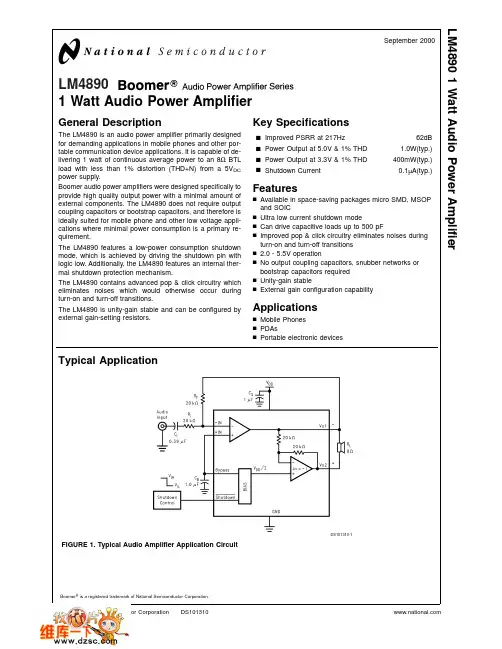
LM48901Watt Audio Power AmplifierGeneral DescriptionThe LM4890is an audio power amplifier primarily designed for demanding applications in mobile phones and other por-table communication device applications.It is capable of de-livering 1watt of continuous average power to an 8ΩBTL load with less than 1%distortion (THD+N)from a 5V DC power supply.Boomer audio power amplifiers were designed specifically to provide high quality output power with a minimal amount of external components.The LM4890does not require output coupling capacitors or bootstrap capacitors,and therefore is ideally suited for mobile phone and other low voltage appli-cations where minimal power consumption is a primary re-quirement.The LM4890features a low-power consumption shutdown mode,which is achieved by driving the shutdown pin with logic low.Additionally,the LM4890features an internal ther-mal shutdown protection mechanism.The LM4890contains advanced pop &click circuitry which eliminates noises which would otherwise occur during turn-on and turn-off transitions.The LM4890is unity-gain stable and can be configured by external gain-setting resistors.Key Specificationsj Improved PSRR at 217Hz 62dB j Power Output at 5.0V &1%THD 1.0W(typ.)j Power Output at 3.3V &1%THD 400mW(typ.)j Shutdown Current0.1µA(typ.)Featuresn Available in space-saving packages micro SMD,MSOP and SOICn Ultra low current shutdown moden Can drive capacitive loads up to 500pFn Improved pop &click circuitry eliminates noises during turn-on and turn-off transitions n 2.0-5.5V operationn No output coupling capacitors,snubber networks or bootstrap capacitors required n Unity-gain stablen External gain configuration capabilityApplicationsn Mobile Phones n PDAsn Portable electronic devicesTypical ApplicationBoomer ®is a registered trademark of National Semiconductor Corporation.DS101310-1FIGURE 1.Typical Audio Amplifier Application CircuitSeptember 2000LM48901Watt Audio Power AmplifierConnection Diagram8Bump micro SMDDS101310-23Top ViewOrder Number LM4890IBP ,LM4890IBPX See NS Package Number BPA08FFBSmall Outline (SO)PackageDS101310-35Top ViewOrder Number LM4890M See NS Package Number M08A Mini Small Outline (MSOP)PackageDS101310-36Top ViewOrder Number LM4890MM See NS Package Number MUA08Amicro SMD MarkingDS101310-70Top View X -Date Code T -Die Traceability G -Boomer Family E -LM4890IBPSO MarkingDS101310-72Top View XY -Date Code TT -Die TraceabilityBottom 2lines -Part NumberMSOP MarkingDS101310-71Top ViewZ -Boomer Family 90-LM4890MML M 4890Absolute Maximum Ratings(Note2)If Military/Aerospace specified devices are required, please contact the National Semiconductor Sales Office/ Distributors for availability and specifications.Supply Voltage 6.0V Storage Temperature−65˚C to+150˚C Input Voltage−0.3V to V DD+0.3V Power Dissipation(Note3)Internally Limited ESD Susceptibility(Note4)2500V ESD Susceptibility(Note5)250V Junction Temperature150˚C Thermal ResistanceθJC(SOP)35˚C/WθJA(SOP)150˚C/WθJA(micro SMD)220˚C/WθJC(MSOP)56˚C/WθJA(MSOP)190˚C/W Soldering InformationSee AN-1112″microSMD Wafers Level Chip Scale Package″.Operating RatingsTemperature RangeT MIN≤T A≤T MAX−40˚C≤T A≤85˚C Supply Voltage 2.0V≤V DD≤5.5VElectrical Characteristics VDD =5V(Notes1,2,8)The following specifications apply for V DD=5V,A V=1,and8Ωload unless otherwise specified.Limits apply for T A=25˚C.Symbol Parameter ConditionsLM4890Units(Limits) Typical Limit(Note6)(Note7)I DD Quiescent Power Supply Current V IN=0V,I o=0A410mA(max) I SD Shutdown Current V shutdown=GND0.1µA(max) P o Output Power THD=2%(max);f=1kHz1W THD+N Total Harmonic Distortion+Noise P o=0.4Wrms;f=1kHz0.1% PSRR Power Supply Rejection Ratio V ripple=200mV sine p-p62(f=217Hz)66(f=1kHz)dBElectrical Characteristics VDD =3.3V(Notes1,2,8)The following specifications apply for V DD=3.3V,A V=1,and8Ωload unless otherwise specified.Limits apply for T A=25˚C.Symbol Parameter ConditionsLM4890Units(Limits) Typical Limit(Note6)(Note7)I DD Quiescent Power Supply Current V IN=0V,I o=0A 3.5mA(max) I SD Shutdown Current V shutdown=GND0.1µA(max) P o Output Power THD=1%(max);f=1kHz0.4W THD+N Total Harmonic Distortion+Noise P o=0.15Wrms;f=1kHz0.1% PSRR Power Supply Rejection Ratio V ripple=200mV sine p-p60(f=217Hz)62(f=1kHz)dBElectrical Characteristics VDD =2.6V(Notes1,2,8)The following specifications apply for V DD=2.6V and8ΩLoad unless otherwise specified.Limits apply for T A=25˚C.Symbol Parameter ConditionsLM4890Units(Limits) Typical Limit(Note6)(Note7)I DD Quiescent Power Supply Current V IN=0V,I o=0A 2.6mA(max)I SD Shutdown Current V shutdown=GND0.1µA(max)LM4890Electrical Characteristics V DD =2.6V(Notes 1,2,8)The following specifications apply for V DD =2.6V and 8ΩLoad unless otherwise specified.Limits apply for T A =25˚C.(Continued)Symbol ParameterConditionsLM4890Units (Limits)Typical Limit (Note 6)(Note 7)P 0Output Power (8Ω)Output Power (4Ω)THD =1%(max);f =1kHz THD =1%(max);f =1kHz 0.20.4W W THD+N Total Harmonic Distortion+Noise P o =0.1Wrms;f =1kHz 0.08%PSRRPower Supply Rejection RatioV ripple =200mV sine p-p44(f =217Hz)44(f =1kHz)dBNote 1:All voltages are measured with respect to the ground pin,unless otherwise specified.Note 2:Absolute Maximum Ratings indicate limits beyond which damage to the device may occur.Operating Ratings indicate conditions for which the device is func-tional,but do not guarantee specific performance limits.Electrical Characteristics state DC and AC electrical specifications under particular test conditions which guar-antee specific performance limits.This assumes that the device is within the Operating Ratings.Specifications are not guaranteed for parameters where no limit is given,however,the typical value is a good indication of device performance.Note 3:The maximum power dissipation must be derated at elevated temperatures and is dictated by T JMAX ,θJA ,and the ambient temperature T A .The maximum allowable power dissipation is P DMAX =(T JMAX –T A )/θJA or the number given in Absolute Maximum Ratings,whichever is lower.For the LM4890,see power derating currents for additional information.Note 4:Human body model,100pF discharged through a 1.5k Ωresistor.Note 5:Machine Model,220pF–240pF discharged through all pins.Note 6:Typicals are measured at 25˚C and represent the parametric norm.Note 7:Limits are guaranteed to National’s AOQL (Average Outgoing Quality Level).Note 8:For micro SMD only,shutdown current is measured in a Normal Room Environment.Exposure to direct sunlight will increase I SD by a maximum of 2µA.External Components Description(Figure 1)Components Functional Description1.R i Inverting input resistance which sets the closed-loop gain in conjunction with R f .This resistor also forms a high pass filter with C i at f C =1/(2πR i C i ).2.C iInput coupling capacitor which blocks the DC voltage at the amplifiers input terminals.Also creates ahighpass filter with R i at f c =1/(2πR i C i ).Refer to the section,Proper Selection of External Components ,for an explanation of how to determine the value of C i .3.R f Feedback resistance which sets the closed-loop gain in conjunction with R i .4.C S Supply bypass capacitor which provides power supply filtering.Refer to the Power Supply Bypassing section for information concerning proper placement and selection of the supply bypass capacitor.5.C BBypass pin capacitor which provides half-supply filtering.Refer to the section,Proper Selection of External Components ,for information concerning proper placement and selection of C B .L M 4890Typical Performance CharacteristicsTHD+N vs Frequencyat V DD=5V,8ΩR L,and PWR=250mWDS101310-37THD+N vs Frequencyat V DD=3.3V,8ΩR L,and PWR=150mWDS101310-38THD+N vs Frequencyat V DD=2.6V,8ΩR L,and PWR=100mWDS101310-39THD+N vs Frequencyat V DD=2.6V,4ΩR L,and PWR=100mWDS101310-40THD+N vs Power OutV DD=5V,8ΩR L,1kHzDS101310-41THD+N vs Power OutV DD=3.3V,8ΩR L,1kHzDS101310-42LM4890Typical Performance Characteristics(Continued)THD+N vs Power Out V DD =2.6V,8ΩR L ,1kHzDS101310-43THD+N vs Power Out V DD =2.6V,4ΩR L ,1kHzDS101310-44Power Supply Rejection Ratio (PSRR)V DD =5VDS101310-45Input terminated with 10ΩRPower Supply Rejection Ratio (PSRR)V DD =5VDS101310-73Input FloatingPower Supply Rejection Ratio (PSRR)V DD =2.6VDS101310-47Input terminated with 10ΩRPower Supply Rejection Ratio (PSRR)V DD =3.3VDS101310-46Input terminated with 10ΩRL M 4890Typical Performance Characteristics(Continued)Power Dissipation vsOutput PowerV DD=3.3VDS101310-49Power Dissipation vsOutput PowerV DD=5VDS101310-48Output Power vsLoad ResistanceDS101310-51Power Dissipation vsOutput PowerV DD=2.6VDS101310-50Supply Current vsShutdown VoltageDS101310-53Clipping(Dropout)Voltage vsSupply VoltageDS101310-52LM4890Typical Performance Characteristics(Continued)Open Loop Frequency ResponseDS101310-55Frequency Response vs Input Capacitor SizeDS101310-54Power Derating Curves DS101310-69Noise FloorDS101310-56L M 4890Application InformationBRIDGE CONFIGURATION EXPLANATIONAs shown in Figure1,the LM4890has two operational am-plifiers internally,allowing for a few different amplifier con-figurations.The first amplifier’s gain is externally config-urable,while the second amplifier is internally fixed in a unity-gain,inverting configuration.The closed-loop gain of the first amplifier is set by selecting the ratio of R f to R i while the second amplifier’s gain is fixed by the two internal10kΩresistors.Figure1shows that the output of amplifier one serves as the input to amplifier two which results in both am-plifiers producing signals identical in magnitude,but out of phase by180˚.Consequently,the differential gain for the IC isA VD=2*(R f/R i)By driving the load differentially through outputs Vo1and Vo2,an amplifier configuration commonly referred to as “bridged mode”is established.Bridged mode operation is different from the classical single-ended amplifier configura-tion where one side of the load is connected to ground.A bridge amplifier design has a few distinct advantages over the single-ended configuration,as it provides differential drive to the load,thus doubling output swing for a specified supply voltage.Four times the output power is possible as compared to a single-ended amplifier under the same condi-tions.This increase in attainable output power assumes that the amplifier is not current limited or clipped.In order to choose an amplifier’s closed-loop gain without causing ex-cessive clipping,please refer to the Audio Power Amplifier Design section.A bridge configuration,such as the one used in LM4890, also creates a second advantage over single-ended amplifi-ers.Since the differential outputs,Vo1and Vo2,are biased at half-supply,no net DC voltage exists across the load.This eliminates the need for an output coupling capacitor which is required in a single supply,single-ended amplifier configura-tion.Without an output coupling capacitor,the half-supply bias across the load would result in both increased internal IC power dissipation and also possible loudspeaker damage. POWER DISSIPATIONPower dissipation is a major concern when designing a suc-cessful amplifier,whether the amplifier is bridged or single-ended.A direct consequence of the increased power deliv-ered to the load by a bridge amplifier is an increase in internal power dissipation.Since the LM4890has two opera-tional amplifiers in one package,the maximum internal power dissipation is4times that of a single-ended amplifier. The maximum power dissipation for a given application can be derived from the power dissipation graphs or from Equa-tion1.P DMAX=4*(V DD)2/(2π2R L)(1)It is critical that the maximum junction temperature T JMAX of 150˚C is not exceeded.T JMAX can be determined from the power derating curves by using P DMAX and the PC board foil area.By adding additional copper foil,the thermal resistance of the application can be reduced from a free air value of 150˚C/W,resulting in higher P DMAX.Additional copper foil can be added to any of the leads connected to the LM4890. It is especially effective when connected to V DD,G ND,and the output pins.Refer to the application information on the LM4890reference design board for an example of good heat sinking.If T JMAX still exceeds150˚C,then additional changes must be made.These changes can include re-duced supply voltage,higher load impedance,or reduced ambient temperature.Internal power dissipation is a functionof output power.Refer to the Typical Performance Charac-teristics curves for power dissipation information for differ-ent output powers and output loading.POWER SUPPLY BYPASSINGAs with any amplifier,proper supply bypassing is critical forlow noise performance and high power supply rejection.The capacitor location on both the bypass and power supply pinsshould be as close to the device as possible.Typical applica-tions employ a5V regulator with10µF tantalum or electro-lytic capacitor and a ceramic bypass capacitor which aid insupply stability.This does not eliminate the need for bypass-ing the supply nodes of the LM4890.The selection of a by-pass capacitor,especially C B,is dependent upon PSRR re-quirements,click and pop performance(as explained in the section,Proper Selection of External Components),sys-tem cost,and size constraints.SHUTDOWN FUNCTIONIn order to reduce power consumption while not in use,theLM4890contains a shutdown pin to externally turn off the amplifier’s bias circuitry.This shutdown feature turns the am-plifier off when a logic low is placed on the shutdown pin.By switching the shutdown pin to ground,the LM4890supplycurrent draw will be minimized in idle mode.While the devicewill be disabled with shutdown pin voltages less than0.5V DC,the idle current may be greater than the typicalvalue of0.1µA.(Idle current is measured with the shutdownpin grounded).In many applications,a microcontroller or microprocessoroutput is used to control the shutdown circuitry to provide a quick,smooth transition into shutdown.Another solution is touse a single-pole,single-throw switch in conjunction with an external pull-up resistor.When the switch is closed,the shut-down pin is connected to ground and disables the amplifier.If the switch is open,then the external pull-up resistor will en-able the LM4890.This scheme guarantees that the shut-down pin will not float thus preventing unwanted state changes.PROPER SELECTION OF EXTERNAL COMPONENTSProper selection of external components in applications us-ing integrated power amplifiers is critical to optimize deviceand system performance.While the LM4890is tolerant of external component combinations,consideration to compo-nent values must be used to maximize overall system qual-ity.The LM4890is unity-gain stable which gives the designer maximum system flexibility.The LM4890should be used inlow gain configurations to minimize THD+N values,and maximize the signal to noise ratio.Low gain configurationsrequire large input signals to obtain a given output power.In-put signals equal to or greater than1Vrms are availablefrom sources such as audio codecs.Please refer to the sec-tion,Audio Power Amplifier Design,for a more complete explanation of proper gain selection.Besides gain,one of the major considerations is the closed-loop bandwidth of the amplifier.To a large extent,the band-width is dictated by the choice of external componentsshown in Figure1.The input coupling capacitor,C i,forms afirst order high pass filter which limits low frequency re-sponse.This value should be chosen based on needed fre-quency response for a few distinct reasons.LM4890Application Information(Continued)Selection Of Input Capacitor SizeLarge input capacitors are both expensive and space hungry for portable designs.Clearly,a certain sized capacitor is needed to couple in low frequencies without severe attenua-tion.But in many cases the speakers used in portable sys-tems,whether internal or external,have little ability to repro-duce signals below 100Hz to 150Hz.Thus,using a large input capacitor may not increase actual system perfor-mance.In addition to system cost and size,click and pop perfor-mance is effected by the size of the input coupling capacitor,C i.A larger input coupling capacitor requires more charge to reach its quiescent DC voltage (nominally 1/2V DD ).This charge comes from the output via the feedback and is apt to create pops upon device enable.Thus,by minimizing the ca-pacitor size based on necessary low frequency response,turn-on pops can be minimized.Besides minimizing the input capacitor size,careful consid-eration should be paid to the bypass capacitor value.Bypass capacitor,C B ,is the most critical component to minimize turn-on pops since it determines how fast the LM4890turns on.The slower the LM4890’s outputs ramp to their quiescent DC voltage (nominally 1/2V DD ),the smaller the turn-on pop.Choosing C B equal to 1.0µF along with a small value of C i (in the range of 0.1µF to 0.39µF),should produce a virtually clickless and popless shutdown function.While the device will function properly,(no oscillations or motorboating),with C B equal to 0.1µF,the device will be much more susceptible to turn-on clicks and pops.Thus,a value of C B equal to 1.0µF is recommended in all but the most cost sensitive de-signs.AUDIO POWER AMPLIFIER DESIGN A 1W/8ΩAUDIO AMPLIFIER Given:Power Output 1WrmsLoad Impedance 8ΩInput Level 1Vrms Input Impedance20k ΩBandwidth 100Hz–20kHz ±0.25dB A designer must first determine the minimum supply rail to obtain the specified output power.By extrapolating from the Output Power vs Supply Voltage graphs in the Typical Per-formance Characteristics section,the supply rail can be easily found.A second way to determine the minimum sup-ply rail is to calculate the required V opeak using Equation 2and add the output ing this method,the minimum supply voltage would be (V opeak +(V OD TOP +V OD BOT )),where V OD BOT and V OD TOP are extrapolated from the Dropout Volt-age vs Supply Voltage curve in the Typical Performance Characteristics section.(2)5V is a standard voltage in most applications,it is chosen for the supply rail.Extra supply voltage creates headroom that allows the LM4890to reproduce peaks in excess of 1W with-out producing audible distortion.At this time,the designer must make sure that the power supply choice along with the output impedance does not violate the conditions explained in the Power Dissipation section.Once the power dissipation equations have been addressed,the required differential gain can be determined from Equa-tion 3.(3)R f /R i =A VD /2From Equation 3,the minimum A VD is 2.83;use A VD =3.Since the desired input impedance was 20k Ω,and with a A VD impedance of 2,a ratio of 1.5:1of R f to R i results in an allocation of R i =20k Ωand R f =30k Ω.The final design step is to address the bandwidth requirements which must be stated as a pair of −3dB frequency points.Five times away from a −3dB point is 0.17dB down from passband response which is better than the required ±0.25dB specified.f L =100Hz/5=20Hz f H =20kHz *5=100kHzAs stated in the External Components section,R i in con-junction with C i create a highpass filter.C i ≥1/(2π*20k Ω*20Hz)=0.397µF;use 0.39µFThe high frequency pole is determined by the product of the desired frequency pole,f H ,and the differential gain,A VD .With a A VD =3and f H =100kHz,the resulting GBWP =150kHz which is much smaller than the LM4890GBWP of 4MHz.This figure displays that if a designer has a need to design an amplifier with a higher differential gain,the LM4890can still be used without running into bandwidth limi-tations.L M 4890Application Information(Continued) HIGHER GAIN AUDIO AMPLIFIERThe LM4890is unity-gain stable and requires no external components besides gain-setting resistors,an input coupling capacitor,and proper supply bypassing in the typical appli-cation.However,if a closed-loop differential gain of greater than10is required,a feedback capacitor(C4)may be needed as shown in Figure2to bandwidth limit the amplifier. This feedback capacitor creates a low pass filter that elimi-nates possible high frequency oscillations.Care should be taken when calculating the-3dB frequency in that an incor-rect combination of R3and C4will cause rolloff before 20kHz.A typical combination of feedback resistor and ca-pacitor that will not produce audio band high frequency rolloff is R3=20kΩand C4=25pf.These components result in a -3dB point of approximately320kHz.It is not recommended that the feedback resistor and capacitor be used to imple-ment a band limiting filter below100kHZ.DS101310-24Figure2LM4890Application Information(Continued)DIFFERENTIAL AMPLIFIERCONFIGURATIONFORLM4890DS101310-29Figure 3L M 4890Application Information(Continued)REFERENCE DESIGN BOARD and LAYOUT-micro SMDDS101310-25Figure4LM4890Application Information(Continued)LM4890micro SMD BOARD ARTWORKSilk ScreenDS101310-57Top LayerDS101310-58Bottom LayerDS101310-59Inner Layer V DDDS101310-60Inner Layer GroundDS101310-61L M 4890Application Information(Continued)REFERENCE DESIGN BOARD and PCB LAYOUT GUIDE-LINES-MSOP&SO BoardsDS101310-68Figure5LM4890Application Information(Continued)LM4890SO DEMO BOARD ARTWORKSilk ScreenDS101310-62Top LayerDS101310-63Bottom LayerDS101310-64LM4890MSOP DEMO BOARD ARTWORKSilk ScreenDS101310-65Top LayerDS101310-66Bottom LayerDS101310-67L M 4890Application Information(Continued)Mono LM4890Reference Design BoardsBill of Material for all3Demo BoardsItem Part Number Part Description Qty Ref Designator 1551011208-001LM4890Mono Reference Design Board110482911183-001LM4890Audio AMP1U120151911207-001Tant Cap1uF16V101C121151911207-002Cer Cap0.39uF50V Z5U201C225152911207-001Tant Cap1uF16V101C330472911207-001Res20K Ohm1/10W53R1,R2,R3 35210007039-002Jumper Header Vertical Mount2X10.1002J1,J2PCB LAYOUT GUIDELINESThis section provides practical guidelines for mixed signal PCB layout that involves various digital/analog power and ground traces.Designers should note that these are only ″rule-of-thumb″recommendations and the actual results will depend heavily on the final layout.General Mixed Signal Layout RecommendationPower and Ground CircuitsFor2layer mixed signal design,it is important to isolate the digital power and ground trace paths from the analog power and ground trace paths.Star trace routing techniques(bring-ing individual traces back to a central point rather than daisy chaining traces together in a serial manner)can have a ma-jor impact on low level signal performance.Star trace routing refers to using individual traces to feed power and ground to each circuit or even device.This technique will take require a greater amount of design time but will not increase the final price of the board.The only extra parts required will be some jumpers.Single-Point Power/Ground ConnectionsThe analog power traces should be connected to the digitaltraces through a single point(link).A″Pi-filter″can be helpfulin minimizing High Frequency noise coupling between theanalog and digital sections.It is further recommended to putdigital and analog power traces over the corresponding digi-tal and analog ground traces to minimize noise coupling.Placement of Digital and Analog ComponentsAll digital components and high-speed digital signals tracesshould be located as far away as possible from analog com-ponents and circuit traces.Avoiding Typical Design/Layout ProblemsAvoid ground loops or running digital and analog traces par-allel to each other(side-by-side)on the same PCB layer.When traces must cross over each other do it at90degrees. Running digital and analog traces at90degrees to eachother from the top to the bottom side as much as possible will minimize capacitive noise coupling and cross talk.LM4890Physical Dimensionsinches (millimeters)unless otherwise notedNote:Unless otherwise specified.1.Epoxy coating.2.63Sn/37Pb eutectic bump.3.Recommend non-solder mask defined landing pad.4.Pin 1is established by lower left corner with respect to text orientation pins are numbered counterclockwise.5.Reference JEDEC registration MO-211,variation BC.8-Bump micro SMDOrder Number LM4890IBP ,LM4890IBPXNS Package Number BPA08FFB X 1=1.412X 2=1.412X 3=0.850L M 4890Physical Dimensions inches(millimeters)unless otherwise noted(Continued)MSOPOrder Number LM4890MMNS Package Number MUA08A LM4890Physical Dimensionsinches (millimeters)unless otherwise noted (Continued)LIFE SUPPORT POLICYNATIONAL’S PRODUCTS ARE NOT AUTHORIZED FOR USE AS CRITICAL COMPONENTS IN LIFE SUPPORT DEVICES OR SYSTEMS WITHOUT THE EXPRESS WRITTEN APPROVAL OF THE PRESIDENT AND GENERAL COUNSEL OF NATIONAL SEMICONDUCTOR CORPORATION.As used herein:1.Life support devices or systems are devices or systems which,(a)are intended for surgical implant into the body,or (b)support or sustain life,and whose failure to perform when properly used in accordance with instructions for use provided in the labeling,can be reasonably expected to result in a significant injury to the user.2.A critical component is any component of a life support device or system whose failure to perform can be reasonably expected to cause the failure of the life support device or system,or to affect its safety or effectiveness.National Semiconductor Corporation AmericasTel:1-800-272-9959Fax:1-800-737-7018Email:support@National Semiconductor EuropeFax:+49(0)180-5308586Email:europe.support@Deutsch Tel:+49(0)6995086208English Tel:+44(0)8702402171Français Tel:+33(0)141918790National Semiconductor Asia Pacific Customer Response Group Tel:65-2544466Fax:65-2504466Email:ap.support@National Semiconductor Japan Ltd.Tel:81-3-5639-7560Email:nsj.crc@ Fax:81-3-5639-7507SOOrder Number LM4890M NS Package Number M08AL M 48901W a t t A u d i o P o w e r A m p l i f i e r。
一种ADS、Cadence软件联合仿真的LNA设计方法谢标;赛景波【摘要】为提高无线通信系统的接收灵敏度,低噪声放大器的设计尤为重要.基于Avago公司的高电子迁移率晶体管ATF54143芯片的2.4G~2.5G ISM频段范围低噪声放大器的设计,采用安捷伦公司的ADS软件设计、制作原理图并进行仿真,然后利用Cadence公司的Allegro SPB软件设计并制作原理图和PCB版图,最后将PCB版图导入到安捷伦公司的ADS系列软件中进行联合仿真,反复调整得到的仿真结果显示放大器工作在绝对稳定状态,噪声系数(NF)低于0.7,增益可达15dB.【期刊名称】《电子设计工程》【年(卷),期】2014(022)003【总页数】5页(P23-27)【关键词】ATF54143;ADS;Cadence;联合仿真【作者】谢标;赛景波【作者单位】北京工业大学电子信息与控制工程学院北京100022;北京工业大学电子信息与控制工程学院北京100022【正文语种】中文【中图分类】TN722.3低噪声放大器(LNA)位于射频接收机的前端,其主要功能是对天线接收到的微弱信号进行放大,减少噪声干扰。
在低噪声放大器的设计过程中,需要综合考虑其放大能力、噪声系数和匹配等因素,这需要大量的理论计算和Smith圆图分析,给设计工作带来困难。
Advanced Design System(ADS)软件是Agilent公司在HPEESOF系列EDA软件基础上发展完善的综合设计软件,内含很多进行小信号放大器设计的控件,能实现大量的计算和Smith圆图分析。
其功能非常强大,仿真手段丰富多样,可实现包括时域和频域、数字与模拟、线性与非线性、噪声等多种仿真分析手段,并可对设计结果进行成品率分析与优化,从而大大提高了复杂电路的设计效率,是非常优秀的微波电路、系统信号链路的设计工具。
Cadence公司的Allegro SPB系列软件具有强大的PCB设计功能,采用以上两种软件联合仿真的设计方法,不仅可以得到比较理想的设计参数,而且发挥了两种软件的长处,成功降低了设计成本,提高设计效率。
IEEETRANSACTIONSONMICROWAVETHEORYANDTECHNIQUES,VOL.58,NO.10,OCTOBER20102575ACompact0.1–14-GHzUltra-WidebandLow-NoiseAmplifierin0.13-mCMOSPo-YuChangandShawnS.H.Hsu,Member,IEEE
Abstract—Acompactultra-widebandlow-noiseamplifier(LNA)witha12.4-dBmaximumgain,a2.7-dBminimumnoisefigure(NF),andabandwidthover0.1–14GHzisrealizedina0.13-mCMOStechnology.Thecircuitisbasicallyaninductorlessconfig-urationusingtheresistive-feedbackandcurrent-reusetechniquesforwidebandandhigh-gaincharacteristics.Itwasfoundthatasmallinductorofonly0.4nHcangreatlyimprovethecircuitperformance,whichenhancesthebandwidthby23%,andreducestheNFby0.94dB(at10.6GHz),whileonlyconsuminganaddi-tionalareaof8080m2.TheLNAonlyoccupiesacoreareaof
0.031mm2,andconsumes14.4mWfroma1.8-Vsupply.
IndexTerms—CMOS,currentreuse,inductorless,low-noiseam-plifier(LNA),resistivefeedback,ultra-wideband(UWB).
I.INTRODUCTION
INRECENTyears,forthedemandofshort-range(within
10m)andhighdata-rate(upto480Mb/s)wirelesscommu-nications,thestandardofultra-wideband(UWB)wassetupbytheFederalCommunicationsCommission(FCC)in2002.TheFCCauthorizedtheunlicensed7.5-GHzband(3.1–10.6GHz)forUWBapplications.Motivatedbyimplementingthetrans-ceiverswithlowcostandahighintegrationlevel,CMOStech-nologybecomesthemostattractivecandidate.OwingtotherapidprogressofCMOStechnology,manystudiesofCMOSRFintegratedcircuits(RFICs)forUWBapplicationswerepub-lishedinsuccessionwithgoodresults[1]–[6].InanUWBreceiver,thelow-noiseamplifier(LNA)withawidebandoperationcapabilityiscriticaltotheoverallreceiverperformance.ThebandwidthoftheLNAisultimatelylimitedbytheparasiticcapacitancesofthedevices.TwotechniquesforextendingthebandwidtharecommonlyusedtodesignUWBLNAsinCMOStechnology,namely,theinductivepeakingtech-niques[1]–[3]andthedistributedamplifier(DA)topology[5].LNAsbasedonthetwotechniqueswerebothreportedwithad-equatebandwidthforUWBapplications.However,onedraw-backisthatthedesignusuallyemploysmanyspiralinductors,whichoccupyalargechiparea.
ManuscriptreceivedJanuary21,2010;revisedJune17,2010;acceptedJune17,2010.DateofpublicationAugust30,2010;dateofcurrentversionOc-tober13,2010.ThisworkwassupportedinpartbyNationalTsingHuaUniver-sity(NTHU)–TaiwanSemiconductorManufacturingCompany(TSMC)underaJoint-DevelopmentProjectandbytheNationalScienceCouncil(NSC)underContractNSC96-2221-E-007-168-MY2,ContractNSC96-2752-E-007-002-PAE,andContract97-2221-E-007-107-MY3.TheauthorsarewiththeDepartmentofElectricalEngineeringandInstituteofElectronicsEngineering,NationalTsingHuaUniversity,Hsinchu300,Taiwan(e-mail:g9561574@oz.nthu.edu.tw;shhsu@ee.nthu.edu.tw).Colorversionsofoneormoreofthefiguresinthispaperareavailableonlineathttp://ieeexplore.ieee.org.DigitalObjectIdentifier10.1109/TMTT.2010.2063832
Recently,inductorlessdesignforwidebandLNAsinCMOStechnologyattractsmuchattentionbecauseoftheconsiderablyreducedchiparea.Variousapproacheswereproposedforwide-bandLNAdesignwithoutusinganyinductors[7]–[12].Thenoise-cancelingtechniquewasadopted[7]–[9],whichsensedthedominantnoisesourceandcanceleditbyanauxiliaryout-of-phaseforwardpathtolowerthenoisefigure(NF).However,thephaseerrorbecomesdifficulttopredict,andthenoisecancel-lationisnotaseffectiveathighfrequencies.Theresistive-feed-backtechniquewasalsoreported[10]–[12].Withalargeenoughinputtransconductance,theresistive-feedbackLNAcanachieveseveralgigahertzofbandwidth,over10-dBgain,andlessthan3-dBNF,butusuallyunderalargebiascurrent[10]orwithamoreadvancedtechnology[12]needed.Tolowerthepowerconsumption,thecurrent-reusetechniqueisemployedtoen-hancetheinputtransconductance[11].Inthisstudy,acompactUWBLNAin0.13-mCMOStech-nologyisproposed.Basedontheconceptofinductorlessdesign,theamplifierincludesaresistive-feedbackconfigurationandacurrent-reuseinputstage.Onesmallinductorofonly0.4nHisemployedatthemostcriticalnode,namely,thegateoftheinputstageoftheLNAtoenhancethebandwidthandlowertheNFsimultaneously.Comparedwiththecircuitwithoutthein-ductor,thebandwidthisincreasedby23%andtheNFisre-ducedby0.94dB(at10.6GHz)withanadditionalareaofonly8080m.TheproposedLNAachievesawideenoughbandwidthtocoverthewhole3.1–10.6-GHzfrequencyrange,a12.4-dBmaximumgain,anda2.7-dBminimumNFwitha0.031mmcoreareaundera14.4-mWpowerconsumption.Thispaperisorganizedasfollows.SectionIIanalyzesthedesigntechniquesinthisstudyincludingresistivefeedbackandgateinductivepeaking.SectionIIIdiscussestheamplifierde-signindetail.SectionIVpresentsthemeasuredresults.Finally,SectionVconcludesthisstudy.
II.TECHNIQUESOFUWBLNADESIGN