A Clock-Gating-Based Test Relaxation and X-Filling Scheme for Reducing Yield Loss Risk
- 格式:pdf
- 大小:745.32 KB
- 文档页数:6
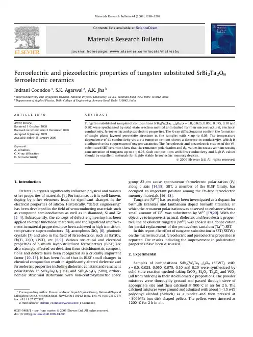
Ferroelectric and piezoelectric properties of tungsten substituted SrBi 2Ta 2O 9ferroelectric ceramicsIndrani Coondoo *,S.K.Agarwal a ,A.K.Jha ba Superconductivity and Cryogenics Division,National Physical Laboratory,Dr K.S.Krishnan Road,New Delhi 110012,India bDepartment of Applied Physics,Delhi College of Engineering,Bawana Road,Delhi 110042,India1.IntroductionDefects in crystals significantly influence physical and various other properties of materials [1].For instance,as it is well known,doping by other elements leads to significant changes in the electrical properties of silicon.Historically,‘‘defect engineering’’has been developed in the field of semiconducting materials such as compound semiconductors as well as in diamond,Si and Ge [2–4].Subsequently,the concept of defect engineering has been applied to other functional materials,and the significant improve-ment in material properties have been achieved in high transition-temperature superconductors [5],amorphous SiO 2[6],photonic crystals [7]and also in the field of ferroelectrics,such as BaTiO 3,Pb(Ti,Zr)O 3(PZT),etc.[8,9].Various structural and electrical properties of bismuth layer-structured ferroelectrics (BLSF)are also strongly affected on deviation from stoichiometric composi-tions and defects have been recognized as a crucially important factor [10–13].It has been found that in BLSF small changes in chemical composition result in significantly altered dielectric and ferroelectric properties including dielectric constant and remanent polarization.In SrBi 2Ta 2O 9(SBT)and SrBi 2Nb 2O 9(SBN),orthor-hombic structural distortions with non-centrosymmetric spacegroup A 21am cause spontaneous ferroelectric polarization (P s )along a axis [14,15].SBT,a member of the BLSF family,has occupied an important position among the Pb-free ferroelectric memory materials [16–18].Tungsten (W 6+)has recently been investigated as a dopant for bismuth titanates and lanthanum doped bismuth titanates,in which the remanent polarization was observed to enhance when a small amount of Ti 4+was substituted by W 6+[19,20].With the objective to improve structural,dielectric and ferroelectric proper-ties,the hexavalent tungsten (W 6+)was chosen as a donor cation for partial replacement of the pentavalent tantalum (Ta 5+)SBT.In this report,the effect of tungsten substitution in SBT (SBTW),on the microstructural,ferroelectric and piezoelectric properties is reported.The results including the improvement in polarization properties have been discussed.2.ExperimentalSamples of compositions SrBi 2(W x Ta 1Àx )2O 9(SBWT),with x =0.0,0.025,0.050,0.075,0.10and 0.20were synthesized by solid-state reaction method taking SrCO 3,Bi 2O 3,Ta 2O 5and WO 3(all from Aldrich)in their stoichiometric proportions.The powder mixtures were thoroughly ground and passed through sieve of appropriate size and then calcined at 9008C in air for 2h.The calcined mixtures were ground and admixed with about 1–1.5wt%polyvinyl alcohol (Aldrich)as a binder and then pressed at $300MPa into disk shaped pellets.The pellets were sintered at 12008C for 2h in air.Materials Research Bulletin 44(2009)1288–1292A R T I C L E I N F O Article history:Received 3October 2008Received in revised form 5December 2008Accepted 6January 2009Available online 15January 2009Keywords:A.CeramicsC.X-ray diffractionD.FerroelectricityA B S T R A C TTungsten substituted samples of compositions SrBi 2(W x Ta 1Àx )2O 9(x =0.0,0.025,0.050,0.075,0.10and 0.20)were synthesized by solid-state reaction method and studied for their microstructural,electrical conductivity,ferroelectric and piezoelectric properties.The X-ray diffractograms confirm the formation of single phase layered perovskite structure in the samples with x up to 0.05.The temperaturedependence of dc conductivity vis-a`-vis tungsten content shows a decrease in conductivity,which is attributed to the suppression of oxygen vacancies.The ferroelectric and piezoelectric studies of the W-substituted SBT ceramics show that the remanent polarization and d 33values increases with increasing concentration of tungsten up to x 0.05.Such compositions with low conductivity and high P r values should be excellent materials for highly stable ferroelectric memory devices.ß2009Elsevier Ltd.All rights reserved.*Corresponding author.Present address:Liquid Crystal Group,National Physical Laboratory,Dr K.S.Krishnan Road,New Delhi 110012,India.Tel.:+919810361727;fax:+911125170387.E-mail address:indrani_coondoo@ (I.Coondoo).Contents lists available at ScienceDirectMaterials Research Bulletinj o ur n a l h o m e p a g e :w w w.e l se v i e r.c om /l oc a t e /m a t r e sb u0025-5408/$–see front matter ß2009Elsevier Ltd.All rights reserved.doi:10.1016/j.materresbull.2009.01.001X-ray diffractograms of the sintered samples were recorded using a Bruker diffractometer in the range 108 2u 708with CuK a radiation.The sintered pellets were polished to a thickness of 1mm and coated with silver paste on both sides for use as electrodes and cured at 5508C for half an hour.Electrical conductivity was performed using Keithley’s 6517A Electrometer.The polarization–electric field (P –E )hysteresis measurements were done at room temperature using an automatic P –E loop tracer based on Sawyer–Tower circuit.Piezoelectric charge co-efficient d 33was measured using a Berlincourt d 33meter after poling the samples in silicone–oil bath at 2008C for half an hour under a dc electric field of 60–70kV/cm.3.Results and discussion3.1.Structural and micro-structural studiesThe phase formation and crystal structure of the ceramics were examined by X-ray diffraction (XRD),which is shown in Fig.1.The XRD patterns of the samples show the characteristic peaks of SBT.The peaks have been indexed with the help of a computer program–POWDIN [21]and the refined lattice parameters are given in Table 1.It is observed that a single phase layered perovskite structure is maintained in the range 0.0 x 0.05.Owing to the same co-ordination number i.e.6and the smallerionic radius of W (0.60A˚)in comparison to Ta (0.64A ˚),there is a high possibility of tungsten occupying the tantalum site.The observance of unidentified peak of very low intensity in the compositions with x >0.05indicates the solubility limit of W concentration in SBT.The unidentified peak is possibly due to tungsten not occupying the Ta sites in the structure as the intensity of this peak is observed to increase with tungsten content.Composition and sintering temperature influences the micro-structure such as grain growth and densification of the specimen,which in turn control other properties of the material [11,13].The effects of W substitution on the microstructure have been examined by SEM and the obtained micrographs are shown in Fig.2.It shows the microstructure of the fractured surface of the studied samples.It is clearly observed that W substitution has pronounced effect on the average grain size and homogeneity of the grains.Randomly oriented and anisotropic plate-like grains are observed in all the samples.It is also observed that the average grain size increases gradually with increasing W content.The average grain size in the sample with x =0.0is $2–3m m while that in the sample with x =0.20the size increases to $5–7m m.3.2.Electrical studiesThe electrical conductivity of ceramic materials encompasses a wide range of values.In insulators,the defects w.r.t.the perfect crystalline structure act as charge carriers and the consideration of charge transport leads necessarily to the consideration of point defects and their migration [22].Many mechanisms were put forward to explain the conductivity mechanism in ceramics.Most of them are approximately divided into three groups:electronic conduction,oxygen vacancies ionic conduction,and ionic and p-type mixed conduction [22].Intrinsic conductivity results from the movement of the component ions,whereas conduction resulting from the impurity ions present in the lattice is known as extrinsic conductivity.At low temperature region (ferroelectric phase),the conduction is dominated by the extrinsic conduction,whereas the conduction at the high-temperature paraelectric phase ($300–7008C)is dominated by the intrinsic ionic conduction [23,25].Fig.3shows the temperature dependence of dc conductivity (s dc )for the undoped and doped SBT samples.The curves show that the conductivity increases with temperature.This is indicative of negative temperature coefficient of resistance (NTCR)behavior,a characteristic of dielectrics [22].It is observed in Fig.3that throughout the temperature range,the dc conductivity of the doped samples are nearly two to three orders lower than that of the undoped sample.Two predominant conduction mechanisms indicated by slope changes in the two different temperature regions are observed in Fig.3.Such changes in the slope in the vicinity of the ferro-paraelectric transition region have been observed in other ferroelectric materials as well [23,24].In addition,it is also observed (Table 2)that the activation energy calculated using the Arrhenius equation [22]in the paraelectric phase increase from $0.80eV for the undoped sample to $2eV for the doped samples.The X-ray photoemission spectroscopic study has confirmed that when Bi 2O 3evaporates during high-temperature processing,vacancy complexes are formed in the (Bi 2O 2)2+layers [26].As a result,defective (Bi 2O 2)2+layers are inherently present in SBT.The undoped SBT shows n-type conductivity,since when oxygen vacancies are created,it leaves behind two trapped electrons [27]:O o !12O 2"þV o þ2e 0(1)where O o is an oxygen ion on an oxygen site,V o is a oxygen vacant site and e 0represents electron.The conductivity in the perovskites can be described as an ordered diffusion of oxygen vacancies [28].Their motion is manifested by enhanced ionic conductivity associated with an activation energy value of $1eV [26].These oxygen vacancies can be suppressed by addition of donors,since the donor oxide contains more oxygen per cation than the host oxide it replaces [29].It has been reported that conductivity in Bi 4Ti 3O 12(BIT)can be significantly decreased,up to three orders of magnitude with the addition of donors,such as Nb 5+and Ta 5+at the Ti 4+sites [23,30].A few other studies on layered perovskites have also reported a decrease inconductivityFig.1.XRD patterns of SrBi 2(W x Ta 1Àx )2O 9samples sintered at 12008C.Table 1Lattice parameters of SrBi 2(W x Ta 1Àx )2O 9samples.Concentration of W a (A ˚)b (A ˚)c (A ˚)0.0 5.5212 5.513924.92230.025 5.5214 5.520225.10790.05 5.5217 5.519925.05850.075 5.5191 5.504525.05670.10 5.5142 5.506125.0850.205.51335.493925.0861I.Coondoo et al./Materials Research Bulletin 44(2009)1288–12921289with addition of donors [23,24,31].In the present study,the Ta 5+-site substitution by W 6+in SBT can be formulated using a defect chemistry expression as WO 3þV o!Ta 2O 512W Ta þ3O o (2)It shows that the oxygen vacancies are reduced upon the substitution of donor W 6+ions for Ta 5+ions.Hence,it is reasonable to believe that the conductivity in SBT is suppressed by donor addition.As per the above discussion,the high s dc observed in the undoped SBT (Fig.3)can be attributed to the motion of oxygen vacancies.As already discussed,the doped samples show reduced conductivity because the transport phenomena involving oxygen vacancies are greatly reduced.The high E a value of $1.75–2eVcorresponding to the high-temperature region in the doped ceramics is consistent with the fact that in the donor-doped materials,the ionic conduction reduces [32].The activation energy E a in the low temperature ferroelectric region (Table 2)corre-sponds to extrinsic conduction.At lower temperatures the extrinsic conductivity results from the migration of impurity ions in the lattice.Some of these impurities may also be associated with lattice defects.Pure SBT has large number of Schottky defects (oxygen vacancies)in addition to impurity ions whereas in the doped samples,due to charge neutrality,there is relatively less content of oxygen vacancies.Thus,in the doped samples the conductivity in the low temperature region is largely due to the impurity ions only.This explains the high activation energy in pure SBT in the low temperature region compared to doped samples (Table 2).In the high-temperature region,the value of E a in the doped samples is observed to increase with W concentration up to x =0.05but beyond that,it decreases (Table 2).The decrease in the activation energy for samples with x >0.05suggests an increase in the concentration of mobile charge carriers [33].This observation can be ascribed to the existence of multiple valence states of tungsten.Since tungsten is a transitional metal element,the valence state of W ions in a solid solution most likely varies from W 6+to W 4+depending on the surrounding chemical environment [34].When W 4+are substituted for the Ta 5+sites,oxygen vacancies would be created,i.e.one oxygen vacancy would be created for every two tetravalent W ions entering the crystal structure,whichFig.3.Variation of dc conductivity with temperature in SrBi 2(W x Ta 1Àx )2O 9samples.Fig.2.SEM micrographs of fractured surfaces of SrBi 2(W x Ta 1Àx )2O 9samples with (a)x =0.0,(b)x =0.025,(c)x =0.050,(d)x =0.075,(e)x =0.10and (f)x =0.20Table 2Activation energy (E a )in the high-temperature paraelectric region and low temperature ferroelectric region;Curie temperature (T c )in SrBi 2(W x Ta 1Àx )2O 9samples.Concentration of W E a (high temp.)(eV)E a (low temp.)(eV)T c (8C)0.00.790.893110.025 1.920.593080.05 1.960.543250.075 1.940.543380.10 1.860.573680.201.740.54390I.Coondoo et al./Materials Research Bulletin 44(2009)1288–12921290explains the increase in the concentration of mobile charge carriers which ultimately results in an decrease in the E a beyond x>0.05. Hence it is reasonable to conclude that W ions in the SBWT exists as a varying valency state,i.e.at lower doping concentration they exist in hexavalent state(W6+)and at a higher doping concentra-tion,they tend to exist in lower valency states[8].The P–E loops of SrBi2(Ta1Àx W x)2O9are shown in Fig.4.It is observed that W-doping results in formation of well-defined hysteresis loops.Fig.5shows the compositional dependence of remanent polarization(2P r)and the coercivefield(2E c)of SrBi2(Ta1Àx W x)2O9samples.Both the parameters depend on W content of the samples.It is observed that2P rfirst increases with x and then decreases while2E cfirst decreases with x and then increases(Fig.5).The optimum tungsten content for maximum2P r ($25m C/cm2)is observed to be x=0.075.It is known that ferroelectric properties are affected by compositional modification,microstructural variation and lattice defects like oxygen vacancies[10,35,36].In hard ferroelectrics, with lower valent substituents,the associated oxide vacancies are likely to assemble in the vicinity of domain walls[37,38].These domains are locked by the defects and their polarization switching is difficult,leading to an increase in E c and decrease in P r[38]. On the other hand,in soft ferroelectrics,with higher valent substituents,the defects are cation vacancies whose generation in the structure generally increases P r.Similar observations have been made in many reports[38–41].Watanabe et al.[42]reported a remarkable improvement in ferroelectric properties in the Bi4Ti3O12ceramic by adding higher valent cation,V5+at the Ti4+ site.It has also been reported that cation vacancies generated by donor doping make domain motion easier and enhance the ferroelectric properties[43].Further,it is known that domain walls are relatively free in large grains and are inhibited in their movement as the grain size decreases[44].In the larger grains, domain motion is easier which results in larger P r.Also for the SBT-based system,it is known that with increase in the grain size the remanent polarization also increases[45,46].Based on the obtained results and above discussion,it can be understood that in the undoped SBT,the oxygen vacancies assemble at sites near domain boundaries leading to a strong domain pinning.Hence,as observed,well-saturated P–E loop for pure SBT is not obtained.But in the doped samples,the suppression of the oxygen vacancies reduces the pinning effect on the domain walls,leading to enhanced remanent polarization and lower coercivefield.Also,the increase in grain size in tungsten added SBT,as observed in SEM micrographs(Fig.2)contribute to the increase in polarization values.In the present study,the grain size is observed to increase with increasing W concentration.However, the2P r values do not monotonously increase and neither the E c decreases continuously with increasing W concentration(Fig.5). The variation of P r and E c beyond x>0.05,seems possibly affected by the presence of secondary phases(observed in XRD diffracto-grams),which hampers the switching process of polarization [47–50].Also,beyond x>0.05the increase in the number of charge carriers in the form of oxygen vacancies leads to pinning of domain walls and thus a reduction in the values of P r and increase in E c is observed.Fig.6shows the variation of piezoelectric charge coefficient d33 with x in the SrBi2(Ta1Àx W x)2O9.The d33values increases with increase in W content up to x=0.05.A decrease in d33values is observed in the samples with x!0.075.The piezoelectric coefficient,d33,increases from13pC/N in the sample with x=0.0to23pC/N in the sample with x=0.05.It is known that the major drawback of SBT is its relatively higher conductivity,which hinders proper poling[51].High resistivity is therefore important for maintenance of poling efficiency at high-temperature[52,53].The W-doped SBT samples show an electrical conductivity value up to three orders of magnitude lower than that of undoped sample(Fig.3).The positional variation of2P r and2E c in SrBi2(W x Ta1Àx)2O9samples.Fig.6.Variation of d33in SrBi2(W x Ta1Àx)2O9samples.Fig. 4.P–E hysteresis loops in SrBi2(W x Ta1Àx)2O9samples recorded at roomtemperature.I.Coondoo et al./Materials Research Bulletin44(2009)1288–12921291decrease in conductivity upon donor doping improve the poling efficiency resulting in the observed higher d33values.Moreover, since the grain size increases with W content in SBT,it is reasonable to believe that the increase in grain size will also contribute to the increase in d33values[54].The decrease in the value of d33for samples with x!0.075is possibly due to the presence of secondary phases as observed in diffractograms[1,51,55]and the increase in oxygen vacancies for samples with x>0.05.4.ConclusionsX-ray diffractograms of the samples reveal that the single phase layered perovskite structure is maintained in the samples with tungsten content x0.05.SEM micrographs reveal that the average grain size increases with increase in W concentration. The temperature dependence of the electrical conductivity shows that tungsten doping results in the decrease of conductivity by up to three order of magnitude compared to W free SBT.All the tungsten-doped ceramics have higher2P r than that of the undoped sample.The maximum2P r($25m C/cm2)is obtained in the composition with x=0.075.The reduced conductivity allows high-temperature poling of the doped samples.Such compositions with low loss and high P r values should be excellent materials for highly stable ferroelectric memory devices.The d33value is observed to increase with increasing W content up to x0.05.The value of d33 in the composition with x=0.05is$23pC/N as compared to$13 pC/N in the undoped sample.AcknowledgmentsThe authors sincerely thank Prof.P.B.Sharma,Dean,Delhi College of Engineering,India for his generous support and providing ample research infrastructure to carry out the research work.The authors are thankful to Dr.S.K.Singhal,Scientist, National Physical Laboratory,India for his fruitful discussion and suggestions.References[1]Y.Noguchi,M.Miyayama,K.Oikawa,T.Kamiyama,M.Osada,M.Kakihana,Jpn.J.Appl.Phys.41(2002)7062.[2]A.Bonaparta,P.Giannozzi,Phys.Rev.Lett.84(2000)3923.[3]S.Connell,E.Siderashaddad,K.Bharuthram,C.Smallman,J.Sellschop,M.Bos-senger,Nucl.Instrum.Methods B85(1994)508.[4]T.Derry,R.Spits,J.Sellschop,Mater.Sci.Bull.11(1992)249.[5]K.Salama,D.F.Lee,Supercond.Sci.Technol.7(1994)177.[6]H.Hosono,Y.Ikuta,T.Kinoshita,M.Hirano,Phys.Rev.Lett.87(2001)175501.[7]S.Noda,A.Chutinan,M.Imada,Nature407(1999)608.[8]S.Shannigrahi,K.Yao,Appl.Phys.Lett.86(2005)092901.[9]G.H.Heartling,nd,J.Am.Ceram.Soc.54(1971)1.[10]H.Watanabe,T.Mihara,H.Yoshimori,C.A.Paz De Araujo,Jpn.J.Appl.Phys.34(1995)5240.[11]T.Atsuki,N.Soyama,T.Yonezawa,K.Ogi,Jpn.J.Appl.Phys.34(1995)5096.[12]T.Noguchi,T.Hase,Y.Miyasaka,Jpn.J.Appl.Phys.35(1996)4900.[13]M.Noda,Y.Matsumuro,H.Sugiyama,M.Okuyama,Jpn.J.Appl.Phys.38(1999)2275.[14]R.E.Newnham,R.W.Wolfe,R.S.Horsey,F.A.D.Colon,M.I.Kay,Mater.Res.Bull.8(1973)1183.[15]A.D.Rae,J.G.Thompson,R.L.Withers,Acta Crystallogr.Sect.B:Struct.Sci.48(1992)418.[16]H.M.Tsai,P.Lin,T.Y.Tseng,J.Appl.Phys.85(1999)1095.[17]Y.Shimakawa,Y.Kubo,Y.Nakagawa,T.Kamiyama,H.Asano,F.Izumi,Appl.Phys.Lett.74(1999)1904.[18]Y.Noguchi,M.Miyayama,T.Kudo,Phys.Rev.B63(2001)214102.[19]J.K.Kim,T.K.Song,S.S.Kim,J.Kim,Mater.Lett.57(2002)964.[20]W.T.Lin,T.W.Chiu,H.H.Yu,J.L.Lin,S.Lin,J.Vac.Sci.Technol.A21(2003)787.[21]Wu E.,POWD,An interactive powder diffraction data interpretation and indexingprogram Ver2.1,School of Physical Science,Flinders University of South Australia, Bedford Park,S.A.JO42AU.[22]R.C.Buchanan,Ceramic Materials for Electronics:Processing,Properties andApplications,Marcel Dekker Inc.,New York,1998.[23]H.S.Shulman,M.Testorf,D.Damjanovic,N.Setter,J.Am.Ceram.Soc.79(1996)3124.[24]M.M.Kumar,Z.G.Ye,J.Appl.Phys.90(2001)934.[25]Y.Wu,G.Z.Cao,J.Mater.Res.15(2000)1583.[26]B.H.Park,S.J.Hyun,S.D.Bu,T.W.Noh,J.Lee,H.D.Kim,T.H.Kim,W.Jo,Appl.Phys.Lett.74(1999)1907.[27]C.A.Palanduz,D.M.Smyth,J.Eur.Ceram.Soc.19(1999)731.[28]C.R.A.Catlow,Superionic Solids&Solid Electrolytes,Academic Press,New York,1989.[29]M.V.Raymond,D.M.Symth,J.Phys.Chem.Solids57(1996)1507.[30]S.S.Lopatin,T.G.Lupriko,T.L.Vasiltsova,N.I.Basenko,J.M.Berlizev,Inorg.Mater.24(1988)1328.[31]M.Villegas,A.C.Caballero,C.Moure,P.Duran,J.F.Fernandez,J.Eur.Ceram.Soc.19(1999)1183.[32]Y.Wu,G.Z.Cao,J.Mater.Sci.Lett.19(2000)267.[33]B.H.Venkataraman,K.B.R.Varma,J.Phys.Chem.Solids66(2005)1640.[34]C.D.Wagner,W.M.Riggs,L.E.Davis,F.J.Moulder,Handbook of X-ray Photoelec-tron Spectroscopy,Perkin Elmer Corp.,Chapman&Hall,1990.[35]Y.Noguchi,I.Miwa,Y.Goshima,M.Miyayama,Jpn.J.Appl.Phys.39(2000)1259.[36]M.Yamaguchi,T.Nagamoto,O.Omoto,Thin Solid Films300(1997)299.[37]W.Wang,J.Zhu,X.Y.Mao,X.B.Chen,Mater.Res.Bull.42(2007)274.[38]T.Friessnegg,S.Aggarwal,R.Ramesh,B.Nielsen,E.H.Poindexter,D.J.Keeble,Appl.Phys.Lett.77(2000)127.[39]Y.Noguchi,M.Miyayama,Appl.Phys.Lett.78(2001)1903.[40]Y.Noguchi,I.Miwa,Y.Goshima,M.Miyayama,Jpn.J.Appl.Phys.39(2000)L1259.[41]B.H.Park,B.S.Kang,S.D.Bu,T.W.Noh,L.Lee,W.Joe,Nature(London)401(1999)682.[42]T.Watanabe,H.Funakubo,M.Osada,Y.Noguchi,M.Miyayama,Appl.Phys.Lett.80(2002)100.[43]S.Takahashi,M.Takahashi,Jpn.J.Appl.Phys.11(1972)31.[44]R.R.Das,P.Bhattacharya,W.Perez,R.S.Katiyar,Ceram.Int.30(2004)1175.[45]S.B.Desu,P.C.Joshi,X.Zhang,S.O.Ryu,Appl.Phys.Lett.71(1997)1041.[46]M.Nagata,D.P.Vijay,X.Zhang,S.B.Desu,Phys.Stat.Sol.(a)157(1996)75.[47]J.J.Shyu,C.C.Lee,J.Eur.Ceram.Soc.23(2003)1167.[48]I.Coondoo,A.K.Jha,S.K.Agarwal,Ferroelectrics326(2007)35.[49]T.Sakai,T.Watanabe,M.Osada,M.Kakihana,Y.Noguchi,M.Miyayama,H.Funakubo,Jpn.J.Appl.Phys.42(2003)2850.[50]C.H.Lu,C.Y.Wen,Mater.Lett.38(1999)278.[51]R.Jain,V.Gupta,A.Mansingh,K.Sreenivas,Mater.Sci.Eng.B112(2004)54.[52]I.S.Yi,M.Miyayama,Jpn.J.Appl.Phys.36(1997)L1321.[53]A.J.Moulson,J.M.Herbert,Electroceramics:Materials,Properties,Applications,Chapman&Hall,London,1990.[54]H.T.Martirena,J.C.Burfoot,J.Phys.C:Solid State Phys.7(1974)3162.[55]R.Jain,A.K.S.Chauhan,V.Gupta,K.Sreenivas,J.Appl.Phys.97(2005)124101.I.Coondoo et al./Materials Research Bulletin44(2009)1288–1292 1292。
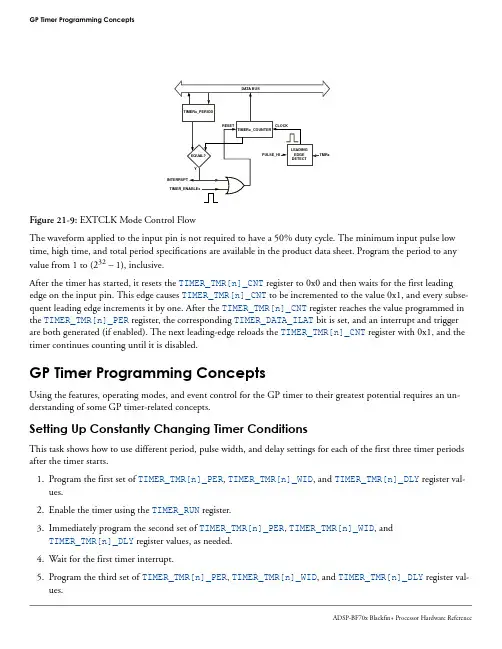
GP Timer Programming ConceptsFigure 21-9: EXTCLK Mode Control FlowThe waveform applied to the input pin is not required to have a 50% duty cycle. The minimum input pulse low time, high time, and total period specifications are available in the product data sheet. Program the period to any value from 1 to (232 – 1), inclusive.After the timer has started, it resets the TIMER_TMR[n]_CNT register to 0x0 and then waits for the first leading edge on the input pin. This edge causes TIMER_TMR[n]_CNT to be incremented to the value 0x1, and every subse-quent leading edge increments it by one. After the TIMER_TMR[n]_CNT register reaches the value programmed in the TIMER_TMR[n]_PER register, the corresponding TIMER_DATA_ILAT bit is set, and an interrupt and trigger are both generated (if enabled). The next leading-edge reloads the TIMER_TMR[n]_CNT register with 0x1, and the timer continues counting until it is disabled.GP Timer Programming ConceptsUsing the features, operating modes, and event control for the GP timer to their greatest potential requires an un-derstanding of some GP timer-related concepts.Setting Up Constantly Changing Timer ConditionsThis task shows how to use different period, pulse width, and delay settings for each of the first three timer periods after the timer starts.1.Program the first set of TIMER_TMR[n]_PER, TIMER_TMR[n]_WID, and TIMER_TMR[n]_DLY register val-ues.2.Enable the timer using the TIMER_RUN register.3.Immediately program the second set of TIMER_TMR[n]_PER, TIMER_TMR[n]_WID, andTIMER_TMR[n]_DLY register values, as needed.4.Wait for the first timer interrupt.5.Program the third set of TIMER_TMR[n]_PER, TIMER_TMR[n]_WID, and TIMER_TMR[n]_DLY register val-ues.measurement report. A measurement report occurs, at most, once per input signal period. The currentTIMER_TMR[n]_CNT value is always copied to the width buffer and period buffer registers at the trailing and lead-ing edges of the input signal, respectively. But, these values are not visible to software. A measurement report event samples the captured values into visible registers and sets the timer interrupt to signal that the TIMER_TMR[n]_PER and the TIMER_TMR[n]_WID registers are ready to be read.When the TIMER_TMR[n]_CFG.TMODE bit =b#1011, the measurement report occurs just after the width buffer register captures its value at a falling edge. Then, the TIMER_TMR[n]_WID register reports the pulse width meas-ured in the pulse that has ended, but the TIMER_TMR[n]_PER register reports the pulse period measured at the end of the previous period. If only the first trailing edge has occurred, then the first period value has not yet been meas-ured at the first measurement report. So, the period value is not valid. A read of the TIMER_TMR[n]_PER value in this case returns 0. See the Example of Width Capture Deasserted Mode (TMODE=b#1011) figure for more infor-mation.SCLK 1TMRx, PULSE_HI =TMRx, PULSE_HI =12356834347121X 843TIMENx212043812X 0X 0X 0X 0COUNTING REPORT REPORT REPORTNOTE: FOR SIMPLICITY, THE SYNCHRONIZATION DELAY BETWEEN TMRx EDGES AND BUFFERREGISTER UPDATES IS NOT SHOWN.TIMER_TMRn_CNT TIMER_TMRn_PER BUFFER TIMER_TMRn_WID BUFFER TIMER_TMRn_PER TIMER_TMRn_WID TIMER_STAT_ILATTIMER_ERR_TYPEFigure 21-3: Example of Width Capture Deasserted Mode (TMODE=b#1011)NOTE :SCLK in the Example of Width Capture Deasserted Mode (TMODE=b#1011) figure is SCLK0.When the TIMER_TMR[n]_CFG.TMODE bit =b#1010, the measurement report occurs just after the period buffer register captures its value at a leading edge. Then, the TIMER_TMR[n]_PER and TIMER_TMR[n]_WID registers re-port the pulse period and pulse width measured in the period that has ended. Refer to the Example of Width Cap-ture Asserted Mode (TMODE=b#1010) figure for more information.GP Timer Operating ModesAfter enabling the timer in this mode, it always starts counting at the asserting edge of the input signal. Any pulse that is already active when the timer is enabled is ignored.With the TIMER_TMR[n]_CFG.IRQMODE bit =b#11, the timer generates an interrupt if the timed pulse width ex-ceeds p MAX , or if the pulse width is less than p MIN . After attaining p MAX , the pulse stays at an active level, and the counter keeps on counting until it sees a de-asserting edge. When the input pulse is not active, the counter holds its current value until it again sees an asserting edge, or it restarts. An interrupt can also be generated for when the pulse occurs within the specified window condition, by setting TIMER_TMR[n]_CFG.IRQMODE =b#10.In this mode, a trailing edge on the input pin triggers capturing of pulse width into the TIMER_TMR[n]_WID regis-ter. During the inactive portion of the input signal, the internal counter does not increment. The Watchdog Width Mode Timing figure shows the signal flow in this mode.TIMER_RUNTMR INTMR_CNTSCLKPmin/TMR_DL Y = 2Pmax/TMR_PER = 5TMR_WID Figure 21-7: Watchdog Width Mode TimingNOTE :SCLK in the Watchdog Width Mode Timing figure is SCLK0.To check only the upper limit on pulse width (p MAX but not p MIN ), then program p MIN as 0 or 1. In such a case, it is better to use TIMER_TMR[n]_CFG.IRQMODE =b#11. With TIMER_TMR[n]_CFG.IRQMODE = b#10, a pulse width of 1 clock cycle results in an interrupt. For details, see the Windowed Watchdog Width Mode Interpretation table.Windowed Watchdog (WATCHDOG) Modes。
一种调节供电进行温度补偿的高精度时钟电路*刘铭扬1,2,3,王小松1,2,3,刘昱1,2,3(1.中国科学院微电子研究所,北京100029;2.中国科学院大学,北京100049;3.新一代通信射频芯片技术北京市重点实验室,北京100029)摘要:基于0.18滋m CMOS标准工艺,实现了一种调节供电电压对温度进行补偿的高精度时钟电路,且有效避免了温度变化及供电波动对振荡频率的影响。
相较于同种类型电路,该结构无需带隙基准源及运算放大器,在优化性能的同时,极大程度地缩减了芯片面积及电路复杂度。
经仿真验证,当温度变化为-40益~85益时,时钟偏差小于1%,可以稳定输出频率为2MHz的时钟信号;当供电由1.6V波动至2.0V时,时钟振荡频率波动仅为28Hz遥关键词:环形振荡器;温度补偿;时钟自校准中图分类号:TN432文献标识码:A DOI:10.16157/j.issn.0258-7998.201026中文引用格式:刘铭扬,王小松,刘昱.一种调节供电进行温度补偿的高精度时钟电路[J].电子技术应用,2021,47(5):117-121.英文弓I用格式:Liu Mingyang,Wang Xiaosong,Liu Yu.A high-precision clock circuit with temperature compensation based on power supply regulation[J].Application of Electronic Technique,2021,47(5):117-121.A high-precision clock circuit with temperature compensationbased on power supply regulationLiu Mingyang1,2,3,Wang Xiaosong1,2,3,Liu Yu1,2,3(1.Institute of Microelectronics of Chinese Academy of Sciences,Beijing100029,China;2.University of Chinese Academy of Sciences,Beijing100049,China;3.Beijing Key Laboratory of Radio Frequency IC Technology for Next Generation Communications,Beijing100029,China) Abstract:Based on0.18Rm CMOS IC process,a high-precision clock circuit that controls power supply voltage to compensatetemperature was presented,which effectively avoids the influence of temperature changes and power supply voltage fluctuations on the oscillation pared with the other types of clock generating circuit,this structure does not require bandgap reference sources and operational amplifier.While optimizing performance,it greatly reduces the chip area and circuit complexity.Under the-40益to85益temperature range,the o utput frequency is stable at2MHz and the clock deviation is less than1%.When the power supply voltage fluctuates from 1.6V to 2.0V,the variation of clock oscillation frequency is28Hz at most.Key words:ring oscillator;temperature compensation;clock self-correction0引言参考时钟于任何模数混合电路而言,都是尤为重要的组成部分。

电子信息、通信、电类专业将会遇到的面试题大全!精!看了让人大吃一惊...模拟电路1、基尔霍夫定理的内容是什么?(仕兰微电子)基尔霍夫电流定律是一个电荷守恒定律,即在一个电路中流入一个节点的电荷与流出同一个节点的电荷相等.基尔霍夫电压定律是一个能量守恒定律,即在一个回路中回路电压之和为零.2、平板电容公式(C=εS/4πkd)。
(未知)3、最基本的如三极管曲线特性。
(未知)4、描述反馈电路的概念,列举他们的应用。
(仕兰微电子)5、负反馈种类(电压并联反馈,电流串联反馈,电压串联反馈和电流并联反馈);负反馈的优点(降低放大器的增益灵敏度,改变输入电阻和输出电阻,改善放大器的线性和非线性失真,有效地扩展放大器的通频带,自动调节作用)(未知)6、放大电路的频率补偿的目的是什么,有哪些方法?(仕兰微电子)7、频率响应,如:怎么才算是稳定的,如何改变频响曲线的几个方法。
(未知)8、给出一个查分运放,如何相位补偿,并画补偿后的波特图。
(凹凸)9、基本放大电路种类(电压放大器,电流放大器,互导放大器和互阻放大器),优缺点,特别是广泛采用差分结构的原因。
(未知)10、给出一差分电路,告诉其输出电压Y+和Y-,求共模分量和差模分量。
(未知)11、画差放的两个输入管。
(凹凸)12、画出由运放构成加法、减法、微分、积分运算的电路原理图。
并画出一个晶体管级的运放电路。
(仕兰微电子)13、用运算放大器组成一个10倍的放大器。
(未知)14、给出一个简单电路,让你分析输出电压的特性(就是个积分电路),并求输出端某点的rise/fall时间。
(Infineon笔试试题)15、电阻R和电容C 串联,输入电压为R和C之间的电压,输出电压分别为C上电压和R 上电压,要求制这两种电路输入电压的频谱,判断这两种电路何为高通滤波器,何为低通滤波器。
当RC<< period - setup ? hold16、时钟周期为T,触发器D1的建立时间最大为T1max,最小为T1min。

简单clock算法
简单的clock算法是一种常用于操作系统中的页面置换算法。
它与FIFO、LRU和最佳置换算法等一样都是常见的置换算法。
基本思路是将物理内存中的页帧组成一个环形链表,每个页框(frame)有一个Use(是否被访问过)和修改位M(是否被修改过)。
当需要置换一个页框时,算法总是从指针指向的位置逐一扫描所有页框:
1. 如果当前页框的Use值为0,直接选择该页框;
2. 如果当前页框的Use值为1,则将其Use为0并继续扫描。
3. 如果所有页框的Use值都为1,则将指针继续转动,重复步骤2和步骤3直到找到一个Use为0的页框。
4. 如果找到一个Use为0的页框,则选择该页框。
5. 如果一轮扫描完毕后,所有页框的Use都为1,则将所有页框的Use都设为0,并从指针的下一个页框重新开始扫描。
这样,可以确保在多次访问中最近没有使用的页框会被优先替换,从而提高内存效率。
而采用此算法还可以通过两次扫描,对所有物理页框分类为2类,每
次回收一类,称之为‘改进型clock算法’。
需要注意的是,clock算法只是一种常用的页面置换算法,实际应用时相应的算法选择还需根据具体情况进行评估和优化。
Published:May 12,2011COMMUNICATION /JACSInterface-Directed Assembly of One-Dimensional Ordered Architecture from Quantum Dots Guest and Polymer HostShengyang Yang,Cai-Feng Wang,and Su Chen*State Key Laboratory of Materials-Oriented Chemical Engineering,and College of Chemistry and Chemical Engineering,Nanjing University of Technology,Nanjing 210009,P.R.ChinabSupporting Information ABSTRACT:Assembly of inorganic semiconductor nano-crystals into polymer host is of great scienti fic and techno-logical interest for bottom-up fabrication of functional devices.Herein,an interface-directed synthetic pathway to polymer-encapsulated CdTe quantum dots (QDs)has been developed.The resulting nanohybrids have a highly uniform fibrous architecture with tunable diameters (ranging from several tens of nanometers to microscale)and enhanced optical performance.This interfacial assembly strategy o ffers a versatile route to incorporate QDs into a polymer host,forming uniform one-dimensional nanomaterials po-tentially useful in optoelectronic applications.Similar to the way that atoms bond to form molecules and complexes,inorganic nanoparticles (NPs)can be combined to form larger ensembles with multidimensional ordered hier-archical architecture,evoking new collective functions.To this end,the development of the controlled self-assembly method for well-de fined structures of these ensembles is signi ficant for creating new and high-performance tunable materials and hence has aroused appealing scienti fic and industrial interest.1Particu-larly,much e ffort has been devoted to the construction of one-dimensional (1D)structures of NPs,owing in part to their application as pivotal building blocks in fabricating a new generation of optoelectronic devices.2In this context,directed host Àguest assembly of NPs into polymer matrices is an e ffective “bottom-up ”route to form 1D ordered functional materials with advantageous optical,electrical,magnetic,and mechanical properties.3Some typical routes have been developed for the generation of these 1D hybrids so far,involving template-assisted,4seeding,5and electro-static approaches.6However,the challenge still remains to precisely manipulate assembly of aqueous NPs and water-insoluble polymers into uniform 1D nanocomposites with a high aspect ratio because of phase separation and aggregation.7Moreover,facile synthetic strate-gies are highly needed to fabricate homogeneous 1D composites in which each component still preserves favorable properties to produce optimal and ideal multifunctional materials.A liquid Àliquid interface o ffers an ideal platform to e fficiently organize NPs into ordered nanostructures driven by a minimiza-tion of interfacial energy.8While much of this research has been directed toward NP hybrids with diverse morphologies based on small organic ligand-directed assembly,9some success has also been achieved in polymer-based NPs nanocomposites.10Russelland co-workers developed ultrathin membranes and capsules of quantum dots (QDs)stabilized by cross-linked polymers at the toluene/water interface.10a,11Brinker ’s group reported the fab-rication of free-standing,patternable NP/polymer monolayer arrays via interfacial NP assembly in a polymeric photoresist.12Herein,a simple host Àguest assembly route is developed to facilely create homogeneous 1D CdTe/polymer hybrids without any indication of phase separation at the aqueous/organic inter-face for the first time.The CdTe nanocrystal is a semiconductor that has been used extensively for making thin film for solar cells.13Some elegant studies have been made in synthesizing pure inorganic 1D CdTe nanowires via assembly from corre-sponding individual CdTe nanocrystals.14In this work,CdTe QDs are covalently grafted with poly(N -vinylcarbazole-co -glycidylmethacrylate)(PVK-co -PGMA)to form uniform fibrous fluorescent composites at the water/chloroform interface via the reaction between epoxy groups of PVK-co -PGMA and carboxyl groups on the surface of CdTe QDs (Scheme 1).15These 1D composite fibers can be allowed to grow further in the radial direction by “side-to-side ”assembly.Additionally,this type of interfacial QD Àpolymer assembly can observably improve the fluorescence lifetime of semiconductor QDs incorporated in theScheme 1.Schematic Representation of the Synthesis of PVK-co -PGMA/CdTe QDs Composite Nano fibersReceived:February 8,2011polymeric matrix.It can be expected that this example of both linear axial organization and radial assembly methodology can be applied to fabricate spatial multiscale organic Àinorganic com-posites with desired properties of NPs and polymers.Figure 1a shows a typical scanning electron microscope (SEM)image of PVK-co -PGMA/CdTe QDs composite nano fi-bers obtained at the water/chloroform interface after dialysis.The as-prepared fibers have uniform diameters of about 250nm and typical lengths in the range of several tens to several hundreds of micrometers (Figures 1a and S4Supporting In-formation [SI]).Interestingly,PVK-co -PGMA/CdTe composite fibers can randomly assemble into nestlike ring-shaped patterns (Figures 1b and S5[SI]).Given the interaction among epoxy groups,the formation of nestlike microstructures could be attributed to incidental “head-to-tail ”assembly of composite fibers.Moreover,in order to establish the relationship between the role of epoxy groups and the formation of composite nano fibers,control experiments were performed,in which pure PGMA or PVK was used to couple CdTe QDs.The PGMA/CdTe composites could be obtained with fibrous patterns (Figure S6[SI]),but no fibrous composites were achieved at the biphase interface with the use of PVK under the same conditions.The microstructures and fluorescence properties of PVK-co -PGMA/CdTe composite fibers were further character-ized using laser confocal fluorescence microscopy (LCFM).Confocal fluorescence micrographs of composite fibers show that the di fferently sized QDs have no obvious in fluence on the morphology of composites (Figure 1c Àe).Clearly,uniform and strong fluorescence emission is seen throughout all the samples,and the size-dependent fluorescence trait of CdTe QDs in PVK-co -PGMA matrix remains well.In order to verify the existence and distribution of CdTe QDs in the fibers,transmission electron microscopy (TEM)was employed to examine the assembled structures.Figure 2a shows a TEM image of PVK-co -PGMA/CdTe QDs composite nano fi-bers,indicating each composite fiber shown in Figure 1a was assembled from tens of fine nano fibers.An individual fine nano fiber with the diameter of about 30nm is displayed in Figure 2b,from which we can see that CdTe QDs have been well anchored into the fiber with polymeric protection layer,revealing this graft-form process at the interface e ffectively avoidednon-uniform aggregation in view of well-dispersed CdTe QDs within the composite fiber,consistent with the LCFM observa-tion.Unlike previous works where the nanoparticles were ad-sorbed onto the polymer fibers,16CdTe QDs were expelled from the surface of fibers (∼2.5nm)in our system (Figure 2c),albeit the high percentage of QDs in the polymer host (23wt %)was achieved (Figure S7[SI]).This peculiarity undoubtedly confers CdTe QDs with improved stability.The clear di ffuse rings in the selected area electron di ffraction (SAED)pattern further indicate excellent monodispersion and finely preserved crystalline struc-ture of QDs in the nano fibers (Figure 2d).The SAED data correspond to the cubic zinc blende structure of CdTe QDs.A possible mechanism for the assembly of 1D nanostructure was proposed,as illustrated in Figure S8[SI].The hydrophilic epoxy groups of the PVK-co -PGMA chain in the oil phase orient toward the biphase interface and then react with carboxyl groups on the surface of CdTe QDs in the aqueous phase to a fford premier PVK-co -PGMA/CdTe QDs composites.Such nanocomposites will reverse repeatedly,resulting from iterative reaccumulation of epoxy groups at the interface and the reaction between the active pieces (i.e.,epoxy or carboxyl groups)in the composites with intact CdTe QDs or PVK-co -PGMA,forming well-de fined nano-fibers.The control experiments showing that the diameter of composite fibers increases with the increase in the concentration of PVK-co -PGMA are in agreement with the proposed mechan-ism (Figure S9[SI]).In addition,it is expected that the pure polymeric layer on the surface of the fibers (red rectangular zone in Figure 2c)will allow further assembly of fine fibers into thick fibers,and these fibers also could randomly evolve into rings,forming nestlike microstructures when the “head ”and “tail ”of fibers accidentally meet (Figure 1b).To further examine the assembly behavior of composite fibers,the sample of PVK-co -PGMA/CdTe QDs composite nano fibers were kept at the water/chloroform interface for an additional month in a close spawn bottle at room temperature (Figure S10[SI]).With longer time for assembly,thicker composite fibers with tens of micrometers in diameter were obtained (Figure 3a).These micro-fibers have a propensityto form twisted morphology (Figure 3a,b),Figure 1.(a,b)SEM images of PVK-co -PGMA/CdTe QDs composite nano fibers.(c Àe)Fluorescence confocal microscopy images of PVK-co -PGMA/CdTe QDs composite nano fibers in the presence of di fferently sized QDs:(c)2.5nm,(d)3.3nm,and (e)3.6nm.The excitation wavelengths are 488(c),514(d),and 543nm (e),respectively.Figure 2.(a,b)TEM images of PVK-co -PGMA/CdTe QDs composite nano fibers,revealing composite nano fiber assemblies.(c)HRTEM image and (d)SAED pattern of corresponding PVK-co -PGMA/CdTe QDs composite nano fibers.while their re fined nanostructures still reveal relatively parallel character and con firm the micro fibers are assembled from countless corresponding nano fibers (Figure 3c).The corresponding LCFM image of an individual micro fiber is shown in Figure 3d (λex =488nm),indicating strong and homogeneous green fluorescence.Another indication is the fluorescent performance of PVK-co -PGMA/CdTe QDs composite micro fibers (Figure 4a).The fluorescent spectrum of composite fibers takes on emission of both PVK-co -PGMA and CdTe QDs,which suggests that this interfacial assembly route is e ffective in integrating the properties of organic polymer and inorganic nanoparticles.It is worth noting that there is a blue-shift (from 550to 525nm)and broadening of the emission peak for CdTe QDs upon their incorporation into polymeric hosts,which might be ascribed to the smaller QD size and less homogeneous QD size distribution resulting from the photooxidation of QD surfaces.17Since the emission spectra of PVK-co -PGMA spectrally overlap with the CdTe QD absorption (Figure S11[SI]),energy transfer from the copolymer to the CdTe QDs should exist.18However,the photoluminescence of PVK-co -PGMA does not vanish greatly in the tested sample in comparison with that of polymer alone,revealing inferior energy transfer between the polymer host and the QDs.Although e fficient energy transfer could lead to hybrid materials that bring together the properties of all ingredients,18it is a great hurdle to combine and keep the intrinsic features of all constituents.19In addition,by changing the polymeric compo-nent and tailoring the element and size of QDs,it should be possible to expect the integration of organic and inorganic materials with optimum coupling in this route for optoelectronic applications.Finally,to assess the stability of CdTe QDs in the composite micro fibers,time-resolved photoluminescence was performed using time-correlated single-photon counting (TCSPC)parative TCSPC studies for hybrid PVK-co -PGMA/CdTe QDs fibers and isolated CdTe QDs in the solid state are presented in Figure 4b.We can see that the presence of PVK-co -PGMA remarkably prolongs the fluorescence lifetime (τ)of CdTe QDs.Decay traces for the samples were well fittedwith biexponential function Y (t )based on nonlinear least-squares,using the following expression.20Y ðt Þ¼R 1exp ðÀt =τ1ÞþR 2exp ðÀt =τ2Þð1Þwhere R 1,R 2are fractional contributions of time-resolved decaylifetimes τ1,τ2and the average lifetime τhcould be concluded from the eq 2:τ¼R 1τ21þR 2τ22R 1τ1þR 2τ2ð2ÞFor PVK-co -PGMA/CdTe QDs system,τh is 10.03ns,which is approximately 2.7times that of isolated CdTe QDs (3.73ns).Photooxidation of CdTe QDs during the assembly process can increase the surface states of QDs,causing a delayed emission upon the carrier recombination.21Also,the polymer host in this system could prevent the aggregation of QDs,avoid self-quench-ing,and delay the fluorescence decay process.22The increased fluorescence lifetime could be also ascribed to energy transfer from PVK-co -PGMA to CdTe QDs.18c The result suggests that this host Àguest assembly at the interface could find signi ficant use in the fabrication of QDs/polymer hybrid optoelectronic devices.In summary,we have described the first example of liquid/liquid interfacial assembly of 1D ordered architecture with the incorporation of the QDs guest into the polymer host.The resulting nanohybrids show a highly uniform fibrous architecture with tunable diameter ranging from nanoscale to microscale.The procedure not only realizes the coexistence of favorable properties of both components but also enables the fluorescence lifetime of QDs to be enhanced.This interesting development might find potential application for optoelectronic and sensor devices due to high uniformity of the 1D structure.Further e fforts paid on optimal regulation of QDs and polymer composition into 1D hybrid nanostructure could hold promise for the integration of desirable properties of organic and inorganic compositions for versatile dimension-dependent applications.In addition,this facile approach can be easily applied to various semiconductor QDs and even metal NPs to develop highly functional 1D nanocomposites.’ASSOCIATED CONTENTbSupporting Information.Experimental details,FT-IR,GPC,UV Àvis,PL,SEM,TGA analysis,and complete ref 9c.This material is available free ofcharge via the Internet at .Figure 3.(a,b)SEM and (c)FESEM images of PVK-co -PGMA/CdTe QDs composite micro fibers.(d)Fluorescence confocal microscopy images of PVK-co -PGMA/CdTe QDs composite micro fibers inthe presence of green-emitting QDs (2.5nm).Figure 4.(a)Fluorescence spectra of PVK-co -PGMA,CdTe QD aqueous solution,and PVK-co -PGMA/CdTe QDs composite micro-fibers.(b)Time-resolved fluorescence decay curves of CdTe QDs (2.5nm diameter)powders (black curve)and the corresponding PVK-co -PGMA/CdTe QDs composite micro fibers (green curve)mea-sured at an emission peak maxima of 550nm.The samples were excited at 410nm.Biexponential decay function was used for satisfactory fitting in two cases (χ2<1.1).’AUTHOR INFORMATIONCorresponding Authorchensu@’ACKNOWLEDGMENTThis work was supported by the National Natural Science Foundation of China(21076103and21006046),National Natural Science Foundation of China-NSAF(10976012),the Natural Science Foundations for Jiangsu Higher Education Institutions of China(07KJA53009,09KJB530005and10KJB5 30006),and the Priority Academic Program Development of Jiangsu Higher Education Institutions(PAPD).’REFERENCES(1)(a)Kashiwagi,T.;Du,F.;Douglas,J.F.;Winey,K.I.;Harris, R.H.;Shields,J.R.Nat.Mater.2005,4,928.(b)Shenhar,R.;Norsten, T.B.;Rotello,V.M.Adv.Mater.2005,17,657.(c)Akcora,P.;Liu,H.; Kumar,S.K.;Moll,J.;Li,Y.;Benicewicz,B.C.;Schadler,L.S.;Acehan, D.;Panagiotopoulos,A.Z.;Pryamitsyn,V.;Ganesan,V.;Ilavsky,J.; Thiyagarajan,P.;Colby,R.H.;Douglas,J.F.Nat.Mater.2009,8,354.(d)Dayal,S.;Kopidakis,N.;Olson,D.C.;Ginley,D.S.;Rumbles,G. J.Am.Chem.Soc.2009,131,17726.(e)Lin,Y.;B€o ker,A.;He,J.;Sill,K.; Xiang,H.;Abetz,C.;Li,X.;Wang,J.;Emrick,T.;Long,S.;Wang,Q.; Balazs,A.;Russell,T.P.Nature2005,434,55.(f)Park,S.;Lim,J.ÀH.; Chung,S.W.;Mirkin,C.A.Science2004,303,348.(g)Mai,Y.; Eisenberg,A.J.Am.Chem.Soc.2010,132,10078.(h)Mallavajula, R.K.;Archer,L.A.Angew.Chem.,Int.Ed.2011,50,578.(i)Kim,J.;Piao, Y.;Hyeon,T.Chem.Soc.Rev.2009,38,372.(2)(a)Xia,Y.;Yang,P.;Sun,Y.;Wu,Y.;Mayers,B.;Gates,B.;Yin, Y.;Kim,F.;Yan,H.Adv.Mater.2003,15,353.(b)Lu,X.;Wang,C.;Wei, Y.Small2009,5,2349.(c)Nie,Z.;Fava,D.;Kumacheva,E.;Zou,S.; Walker,G.C.;Rubinstein,M.Nat.Mater.2007,6,609.(3)(a)Huynh,W.U.;Dittmer,J.J.;Alivisatos,A.P.Science2002, 295,2425.(b)Balazs,A.C.;Emrick,T.;Russell,T.P.Science2006, 314,1107.(c)Ramanathan,T.;Abdala,A.A.;Stankovich,S.;Dikin, D.A.;Herrera-Alonso,M.;Piner,R.D.;Adamson,D.H.;Schniepp, H.C.;Chen,X.;Ruoff,R.S.;Nguyen,S.T.;Aksay,I.A.;Prud’homme, R.K.;Brinson,L.C.Nat.Nanotechnol.2008,3,327.(d)Tomczak,N.; Janczewski,D.;Han,M.;Vancso,G.J.Prog.Polym.Sci.2009,34,393.(e)Zhao,Y.;Thorkelsson,K.;Mastroianni,A.J.;Schilling,T.;Luther, J.M.;Rancatore,B.J.;Matsunaga,K.;Jinnai,H.;Wu,Y.;Poulsen,D.; Frechet,J.M.J.;Alivisatos,A.P.;Xu,T.Nat.Mater.2009,8,979.(f) Colfen,H.;Mann,S.Angew.Chem.,Int.Ed.2003,42,2350.(g)Sone,E.D.;Stupp,S.I.J.Am.Chem.Soc.2004,126,12756.(4)Chan,C.S.;De Stasio,G.;Welch,S.A.;Girasole,M.;Frazer,B.H.;Nesterova,M.V.;Fakra,S.;Banfield,J.F.Science2004,303,1656.(5)Tran,H.D.;Li,D.;Kaner,R.B.Adv.Mater.2009,21,1487.(6)Yuan,J.;M€u ller,A.H.E.Polymer2010,51,4015.(7)(a)Greenham,N.C.;Peng,X.;Alivisatos,A.P.Phys.Rev.B 1996,54,17628.(b)Lopes,W.A.;Jaeger,H.M.Nature2001,414,735.(c)Gupta,S.;Zhang,Q.;Emrick,T.;Balazs,A.Z.;Russell,T.P.Nat. Mater.2006,5,229.(8)(a)Wang,X.;Zhuang,J.;Peng,Q.;Li,Y.Nature2005,437,121.(b)Huang,J.;Kaner,R.B.J.Am.Chem.Soc.2004,126,851.(c)Binder, W.H.Angew.Chem.,Int.Ed.2005,44,5172.(d)Capito,R.M.;Azevedo, H.S.;Velichko,Y.S.;Mata,A.;Stupp,S.I.Science2008,319,1812.(e)Yin,Y.;Skaff,H.;Emrick,T.;Dinsmore,A.D.;Russell,T.P.Science 2003,299,226.(f)Arumugam,P.;Patra,D.;Samanta,B.;Agasti,S.S.; Subramani,C.;Rotello,V.M.J.Am.Chem.Soc.2008,130,10046.(g)Hou,L.;Wang,C.F.;Chen,L.;Chen,S.J.Mater.Chem.2010, 20,3863.(9)(a)Duan,H.;Wang,D.;Kurth,D.G.;Mohwald,H.Angew. Chem.,Int.Ed.2004,43,5639.(b)B€o ker,A.;He,J.;Emrick,T.;Russell,T.P.Soft Matter2007,3,1231.(c)Russell,J.T.;et al.Angew.Chem.,Int. Ed.2005,44,2420.(10)(a)Lin,Y.;Skaff,H.;B€o ker,A.;Dinsmore,A.D.;Emrick,T.; Russell,T.P.J.Am.Chem.Soc.2003,125,12690.(b)B€o ker,A.;Lin,Y.; Chiapperini,K.;Horowitz,R.;Thompson,M.;Carreon,V.;Xu,T.; Abetz,C.;Skaff,H.;Dinsmore,A.D.;Emrick,T.;Russell,T.P.Nat. Mater.2004,3,302.(11)Skaff,H.;Lin,Y.;Tangirala,R.;Breitenkamp,K.;B€o ker,A.; Russell,T.P.;Emrick,T.Adv.Mater.2005,17,2082.(12)Pang,J.;Xiong,S.;Jaeckel,F.;Sun,Z.;Dunphy,D.;Brinker,C.J.J.Am.Chem.Soc.2008,130,3284.(13)Fulop,G.;Doty,M.;Meyers,P.;Betz,J.;Liu,C.H.Appl.Phys. Lett.1982,40,327.(14)(a)Tang,Z.;Kotov,N.A.;Giersig,M.Science2002,297,237.(b)Zhang,H.;Wang,D.;Yang,B.;M€o hwald,H.J.Am.Chem.Soc.2006, 128,10171.(c)Yang,P.;Ando,M.;Murase,N.Adv.Mater.2009, 21,4016.(d)Srivastava,S.;Santos,A.;Critchley,K.;Kim,K.-S.; Podsiadlo,P.;Sun,K.;Lee,J.;Xu,C.;Lilly,G.D.;Glotzer,S.C.;Kotov, N.A.Science2010,327,1355.(15)Reis,A.V.;Fajardo,A.R.;Schuquel,I.T.A.;Guilherme,M.R.; Vidotti,G.J.;Rubira,A.F.;Muniz,.Chem.2009,74,3750.(16)(a)Djalali,R.;Chen,Y.;Matsui,H.J.Am.Chem.Soc.2002, 124,13660.(b)George,J.;Thomas,K.G.J.Am.Chem.Soc.2010, 132,2502.(17)(a)Yang,S.;Li,Q.;Chen,L.;Chen,S.J.Mater.Chem.2008, 18,5599.(b)Wang,Y.;Herron,N.J.Phys.Chem.1991,95,525.(c)Zhang,Y.;He,J.;Wang,P.N.;Chen,J.Y.;Lu,Z.J.;Lu,D.R.;Guo,J.; Wang,C.C.;Yang,W.L.J.Am.Chem.Soc.2006,128,13396.(d)Carrillo-Carri o n,C.;C a rdenas,S.;Simonet,B.M.;Valc a rcel,M. mun.2009,5214.(18)(a)Tessler,N.;Medvedev,V.;Kazes,M.;Kan,S.;Banin,U. Science2002,295,1506.(b)Zhang,Q.;Atay,T.;Tischler,J.R.;Bradley, M.S.;Bulovi c,V.;Nurmikko,A.V.Nat.Nanotechnol.2007,2,555.(c)Lutich,A.A.;Jiang,G.X.;Susha,A.S.;Rogach,A.L.;Stefani,F.D.; Feldmann,J.Nano Lett.2009,9,2636.(19)Li,M.;Zhang,J.;Zhang,H.;Liu,Y.;Wang,C.;Xu,X.;Tang,Y.; Yang,B.Adv.Funct.Mater.2007,17,3650.(20)Schr€o der,G.F.;Alexiev,U.;Grubm€u ller,H.Biophys.J.2005, 89,3757.(21)(a)Zhong,H.Z.;Zhou,Y.;Ye,M.F.;He,Y.J.;Ye,J.P.;He,C.; Yang,C.H.;Li,Y.F.Chem.Mater.2008,20,6434.(b)Sun,H.;Zhang, H.;Zhang,J.;Ning,Y.;Yao,T.;Bao,X.;Wang,C.;Li,M.;Yang,B. J.Phys.Chem.C2008,112,2317.(22)Kagan,C.R.;Murray,C.B.;Bawendi,M.G.Phys.Rev.B1996, 54,8633.。

Runner and gate design.The Important FeaturesIntroduction;The following is a brief summary of the important factors to consider when designing runner and gating systems for Zinc and Aluminium pressure die casting dies.In the past runner systems were designed using empirical knowledge and developed using trial and error methods which involved excessive time and often multiple die trials. Today, computer programmes exist which eliminate these problems and are able to give good results immediately but, many of the most basic design issues are often neglected during the design stage particularly if the die is designed by the tool maker without consultation to the die casting technicians.These brief notes are intended as guidelines for use during training and as an aide memoiré for die design technicians and designers. They are not intended to cover all aspects of die design practice.____________________________Objective:The runner and gate system should achieve the following in basic terms:•Produce a casting of the specified quality; in terms of finish, size and tolerance, casting integrity, mechanical properties, cycle time and consistency.••Achieve first time success; to avoid wasted time on successive machine trials, delays in delivery of samples, loss of customer confidence and excessive die developmentcosts.••Provide optimum yield; increases efficiency by optimising the casting to runner yield ratio, improve metal losses due to lower re-melt weights, reduces cycle times due toimproved thermal efficiency.THE BROCK METAL COMPANY LIMITED,WALSALL ROAD. NORTON CANES, CANNOCK, STAFFS, UK WS11 9NR.Runner and gate design.Influencing factors.Designing a runner system:Selection of the machine should be based on several factors but not just shot weight and platen area. Most machines are supplied with a PQ2 diagram or one exists from measurements taken on other similar machines. Runner designs should be based on machine performance with a given plunger or shot sleeve diameter, known hydraulic pressure and in the case of hot chamber die casting the nozzle size. Both projected area and lock tonnage should also be considered if the proposed runner plus casting is liable to approach the machine limits.Casting geometry:The cavity should be positioned to promote the best cavity fill conditions while accommodating essential die features such as core slides, cooling channels, sensitive casting features, number of cavities and robotic removal constraints. Other process criteria such as second operation locations, clipping orientation, break off de-gating and finishing requirements should also be considered before the cavity position is decided.Uniform flow path:The runner should establish a uniform metal flow rate deigned to promote the best hydraulic system, stable metal pressure and velocity. Most computer design programmes will control these features but the designer will still have institute a flow path allows these features conform to the desired parameters.Cavity fill conditions:Modern pressure die casting machines often have more power at the shot end than is required to achieve the optimum fill conditions. Consequently, the performance offers many gate area options capable of achieving the desired fill conditions – the designer must select the most suitable based on the casting specification and process limitations.Cavity fill pattern:Is invariably decided by the casting geometry and gate position but the metal pressure and velocity will have influence but to a lesser extent. The influence of casting features such as vertical surfaces and ribs, variable section thicknesses, isolated bosses and cores must be considered when the gate position is decided.Venting and overflow wells:Should all be considered at the design stage – are directly related to the cavity fill conditions and casting geometry but also the introduction of over flow wells or pockets may have significant cost implications.THE BROCK METAL COMPANY LIMITED,WALSALL ROAD. NORTON CANES, CANNOCK, STAFFS, UK WS11 9NR.Runner and gate design.Machine Performance.Effects of change.Injection pressure: Reduce or increase .• Increased injection pressure – will increase flash, raise galvanising and die erosion.Optimum pressure levels will improve casting integrity, maintain speed and velocity and improve cavity fill conditions.Reduced injection pressure – reduces flow rates, and static metal pressure on hot chamber pressure die casting machines.• Plunger diameter – on hot chamber die casting machines smaller plungers give thebest casting results with higher injection pressure and faster delivery. On aluminium cold chamber machines plunger diameter choice is less critical but effect is far more significant in performance terms - increasing delivery velocity and reducing cavity fill times.• Plunger speeds - high terminal velocities can produce pressure spikes on older diecasting machines leading flash and die wear. High gate speeds result in expensive die maintenance due to die erosion and galvanising.• Runner Area/volume - die designer should create a uniform flow through the runnerby establishing nozzle area (hot chamber) as the largest section in the runner.Progressively reducing the cross sectional area of the runner at each section to the gate which should be the smallest area in the runner system. Similarly, on cold chamber dies the sprue post runner should be the largest runner section down to the gate which should be smallest section of the runner.Flow rate histogram.N o z z l e a r e aGateAreaTHE BROCK METAL COMPANY LIMITED,WALSALL ROAD. NORTON CANES, CANNOCK, STAFFS, UK WS11 9NR.Runner and gate design.Runner features‘Y’ Junction not ‘T’‘Y’ JunctionReduces area and increases pressure progressively.‘T’ JunctionIncreases volume at the junction creating low pressure area at the centre of the gate.THE BROCK METAL COMPANY LIMITED,WALSALL RO D. NORTON CANES, CANNOCK, STAFFS, UK WS11 9NR.ARunner and gate design .Runner featuresTaper tangential runner - with shock absorber – showing section change A to B toSmaller diagram – illustrates poor runner design small access radius,increased e taper,maintain pressure and velocityrunner volume at the radius, small runner cross section at the end of th and no shock absorber.THE BROCK METAL COMPANY LIMITED,WALSALL RO D. NORTO NES, CANNOCK, STAFFS, UK WS11 9NR.A N CARunner and gate design .Runner featuresDrawings – Show section through sprue posts on Aluminium (top ) and Zinc (bottom )This area most commonly inte d incorrectly by toolmakers.Note; Th radiusdies.rprete e reduction from the sprue faces to die face and the size and blend which are struck from the same centre to ensure even transition from sprue to die.THE BROCK METAL COMPANY LIMITED, WALSALL ROAD,. NORTON CANES, CANNOCK, STAFFS, UK WS11 9NR.Runner and gate design .Runner featuresRunner sections: Need to be adjusted by differing percentages tor l10% reduction in runnerarea- down stream of metalaccommodate larger angular direction changes30% reduction in runner a ea - down stream of meta flow – for 900 bend.flow – for a 200 bend.THE BROCK METAL COMPANY LIMITED, WALSALL ROAD. NORTON CANES, CANNOCK, STAFFS, UK WS11 9NR,Runner and gate design .Gate Areasate Areas:ptimum for Zinc alloy pressure die-casting :ed / velocity – 35 – 45 metres per second.ish – 20 milli seconds or functionalOptimum for Aluminium alloy pressure die casting:5 metres per second..ortant on large castings asFil a etry: has the largest influence on cavity flow paths – high metal velocitypplied to vertical casting faces causes turbulence, galvanising and impedes metal. All of which and areas; It is possible to assess parts of the casting separately nd this may be advantageous if they are unlikely to be fed directly from the gate. of a given part sing separate gates for each zoned area. This will often improve fill characteristics low: It must be stressed that the gates and runner both fluence flow direction. Once the runner is established metal under pressure will G O • Gate spe • Cavity fill time – plated or powder coated fin parts – 40 milli seconds.• Gate depth – 0.15 – 0.5 mm.• Gate speed / velocity – 25 to 3To avoid die erosion and control cavity fill characteristics • Cavity fill time – end of fill temperature is most imp solidification can occur prior to cavity filling.• Depth 1.25 – 3 mm (1.5 mm minimum for machine intensification to be effective ).l P ttern:Casting geom a can result in expensive die repairs / maintenance. Section changes and cores change pressure and direction and these effects need to be considered and understood when considering gate position options.Zones volumes a Using computer programmes allows each separate zone to be quantified in volume and surface area terms. If treated as un-gated the fill time and end of fill temperature can be determined as a comparison with the main body of the total casting.Gating separate zones: It is possible also to examine separate zones u and reduce the risks of defects. The uses of multiple gates are not a risk if designed and implemented correctly.Runner will direct metal f in enter the cavity in the same direction and flow angle. Varying injection speed and metal pressure may alter this angle slightly but this is only a fine tuning method.THE BROCK METAL COMPANY LIMITED, WALSALL ROAD. NORTO NES, CANNOCK, STAFFS, UK WS11 9NR,N CARunner and gate design .Fill pattern.Influence of casting geometry ertain casting shapes are best filled in a predetermined way, if the toolingre the depth is 50% of the edge length or more he box :C configuration allows. Deep boxes, whe can be fed using the gate runner configuration shown below – alternatively t can be turned through 450 to shorten the runner distance and improve shot yield.THE BROCK METAL COMPANY LIMITED, WALSALL ROAD. NORTON CANES, CANNOCK, STAFFS, UK WS11 9NR,Runner and gate design .Fill pattern.vals or round castings: Try to fill the centre first using either a runneronfiguration below or a more traditional fan feed. With fan feeds it is essential to getO c the ratio of the approach angle and width of gate correct.THE BROCK METAL COMPANY LIMITED, WALSALL ROAD. NORTON CANES, CANNOCK, STAFFS, UK WS11 9NR,Runner and gate design .Fill pattern.nnular rings: Can be fed using the runner configuration indicated below. A smallver flow well should positioned in the centre hole to take away any lubrication fume A o and another well placed on the out side perimeter adjacent to the last segment of the part to fill.THE BROCK METAL COMPANY LIMITED, WALSALL ROAD. NORTON CANES, CANNOCK, STAFFS, UK WS11 9NR,Runner and gate design .Fill pattern.Rectangular Plates: Fill across shortest distance whenever possible – t cut downow distance and increase end of fill temperature. It is therefore advisable to avoido fl the option shown in the upper diagram if possible.THE BROCK METAL COMPANY LIMITED, WALSALL ROAD. NORTON CANES, CANNOCK, STAFFS, UK WS11 9NR,Runner and gate design .Fill pattern.Diagram show e – to resolve problems ofporosity and poor ximately 6 mm deep, with a gate depth of between 1.8 and 2.5 mm. Casting weighed approximately 5 Kg and with a flow distance of 510 m s: runner developed over a period of tim fill results. The darker blue area is appro m.THE BROCK METAL COMPANY LIMITED, WALSALL ROAD. NORTON CANES, CANNOCK, STAFFS, UK WS11 9NR,Runner and gate design .Fill pattern.Diagram show niform gate thickness of 2 mm. The runner and a subsequent increase in yield of 18% and a reduction in pr ected area of some 22% allowing improved shot speed and increased in injecs: Revised runner with balance fill and u shows reduced shot weight by over 1 Kg oj tion pressure.THE BROCK METAL COMPANY LIMITED, WALSALL ROAD. NORTON CANES, CANNOCK, STAFFS, UK WS11 9NR,Runner and gate design .Vents and Overflow wells.Points to remember:• Over flow w tal flow, but rarely remove gas and fume as the cavity is normal sealed before they become a .only work for less than half of the cavity fill time as they arefinal fill is achieved. • Over flow wells are a poor method of die heating both inefficient and wasteful.See reference material from ILZRO, IZA.JWTSep ells can be used to change or divert mective ly • Similarly vents can sealed off before the• Use only one connection per over flow to avoid back feeding through theoverflow and reintroducing gas and cold metal. • Always vent over flow wells – as a precaution.Many are lost before re-melting and therefore increase metal losses.t 05 – issue 5。
(上海华虹)1、国家211工程本科以上,电子类相关专业,外貌具有亲和力2、较强的逻辑思维能力,语言表达能力,善于撰写报告3、勇于承受工作压力和挫折、随机应变4、熟悉mcu软、硬件应用,具备独立开发能力优先5、熟悉模拟电路应用,具备产品开发和应用能力优先(华为)1。
集成电路设计前端流程及工具。
答:前端流程主要是RTL级设计,验证,综合。
后端主要是布图布线综合后的输出文件,可以拿去做layout,将电路fit到可编程的片子里或者布道硅片上,这分单元库和全定制。
单元库下一步就是自动布局布线,auto place & route,简称apr cadence的工具是Silicon Ensembler,Avanti的是Apollo;全定制Cadence的工具是layout editor。
2。
FPGA和ASIC的概念,他们的区别答:FPGA是可编程ASIC;ASIC:专用集成电路,它是面向专门用途的电路,专门为一个用户设计和制造的。
根据一个用户的特定要求,能以低研制成本,短交货周期供货的全定制,半定制集成电路。
与门阵列等其它ASIC相比,它们又具有设计开发周期短,设计制造成本低,开发工具先进、标准产品无需要测试、质量稳定以及可实时在线检验等优点。
3。
LATCH和DFF的概念和区别答:LATCH和DFF都是时序逻辑,区别为:latch同其所有的输入信号相关,当输入信号变化时latch就变化,没有时钟端;DFF受时钟控制,只有在时钟触发时才采样当前的输入,产生输出。
当然因为二十都是时序逻辑,所以输出不但用当前的输入相关还同上一时间的输出相关。
4。
用DFF实现二分频。
答:module div2(input wire en _ n, input wire out _ clk);Wire D;Wire Q;Assign D=en _n & (~Q);DFF (.clk (clk), .D(D), .Q(Q));Assign out _ clk =Q;endmodule5。
CTX: A Clock-Gating-Based Test Relaxation and X-Filling Scheme for Reducing Yield Loss Risk in At-Speed Scan Testing
H. Furukawa 1, X. Wen 1, K. Miyase 1, Y. Yamato 1, S. Kajihara 1, P. Girard 2, L.-T. Wang 3, and M. Tehranipoor 4 1 Kyushu Institute of Technology, Iizuka, Fukuoka 820-8502, Japan
2 LIRMM, 161 rue Ada, 34392 Montpellier cedex 05, France
3 SynTest Technologies, Inc., Sunnyvale, CA 94086, USA
4 University of Connecticut, Storrs, CT 06269, USA
Abstract At-speed scan testing is susceptible to yield loss risk due to power supply noise caused by excessive launch switching activity. This paper proposes a novel two-stage scheme, namely CTX (Clock-Gating-Based Test Relaxation and X-
Filling), for reducing switching activity when test stimulus is launched. Test relaxation and X-filling are conducted (1) to make as many FFs inactive as possible by disabling corresponding clock-control signals of clock-gating circuitry in Stage-1 (Clock-Disabling), and (2) to make as many remaining active FFs as possible to have equal input and output values in Stage-2 (FF-Silencing). CTX effectively reduces launch switching activity, thus yield loss
risk, even with a small number of don’t care (X) bits as in test compression, without any impact on test data volume, fault coverage, performance, and circuit design. Keywords: Power Supply Noise, Test Relaxation, X-Filling, Clock-Gating, Test Compaction.
1. Introduction At-speed scan testing is mandatory for improving timing-related test quality [1]. It is realized by launching a transition at the start-point of a path and capturing its response at the end-point of the path at the system speed. In practice, the launch-on-capture (LOC) clocking scheme is widely used for at-speed scan testing [1].
Load CompletedTransitionResponseLoad StartedShift ModeS1C2C1SLCKSETest VectorLaunchCaptureTest CycleTest VectorCapture Mode
Rated System Clock Period Fig. 1 LOC-Based At-Speed Scan Testing. Fig. 1 shows the essence of the LOC clocking scheme: After a test vector is loaded by a series of shift clock pulses with SL being the last one (L: the length of the longest scan
chain), transitions are launched by the first capture clock pulse C1 at the corresponding scan FFs. The transitions are caused by the difference between the values shifted-in by SL and the values captured by C1. The test cycle between the
transition launch (C1) and the response capture (C2) is the rated system clock period.
Although at-speed scan testing is indispensable for improving timing-related test quality [1], its applicability is being severely challenged by test-induced yield loss, which occurs when functionally good chips fail only during at-speed scan testing [2-4]. The major cause for this problem is power supply noise, i.e., IR-drop and ground bounce, caused by excessive launch switching activity at C1, which
results in delay increase. It has been shown that a 10% drop in power supply voltage can increase path delay by 30% [5]. Obviously, this may result in capture failures at C2 [4], thus
leading to test-induced yield loss [6-8]. This problem is deteriorating rapidly for deep-submicron and low-power chips [6]. Therefore, there is a strong need to reduce the yield loss risk induced by excessive power supply noise.
Previous techniques for reducing launch switching activity are based on the following three approaches: (1) Partial Capture: The number of FFs that capture at C1
(Fig. 1) can be reduced by circuit modification [9],
one-hot clocking [1], or capture clock staggering [1]. However, this approach may incur significant ATPG change, test data inflation, and even fault coverage loss. (2) Low-Capture-Power ATPG: 0’s and 1’s in a test
vectors can be carefully generated so that launch switching activity is reduced by such techniques as input-output equalizing at FFs [10], clock-gating, etc. However, this approach may suffer from significant test data inflation and long CPU time. (3) Test Relaxation & X-Filling: Test relaxation is to identify don’t-care bits (X-bits) from a set of fully-specified test vectors without any fault coverage loss [11, 12]. Then, X-filling is conducted on the resulting partially-specified test cubes to make as many FFs as possible to have equal input and output values [13-15]. This way, launch switching activity is reduced. The concept of this approach is illustrated in Fig. 2.
c0100a1100Test Vector SetTest Vector SetSame FaultTest Relaxationv1v2v3v4b1011Same FaultCoverageInitialIntermediateTest Cube SetFinalv’1v’2v’3v’4Coveragev”1v”2