Symbol
t ≤ 10s Steady-State Steady-State
R θJL
Units V W V °C/W R θJA 48mJ Units 62.5°C
A A Max Maximum Junction-to-Ambient A Thermal Characteristics
Parameter
Typ Maximum Junction-to-Lead
°C/W
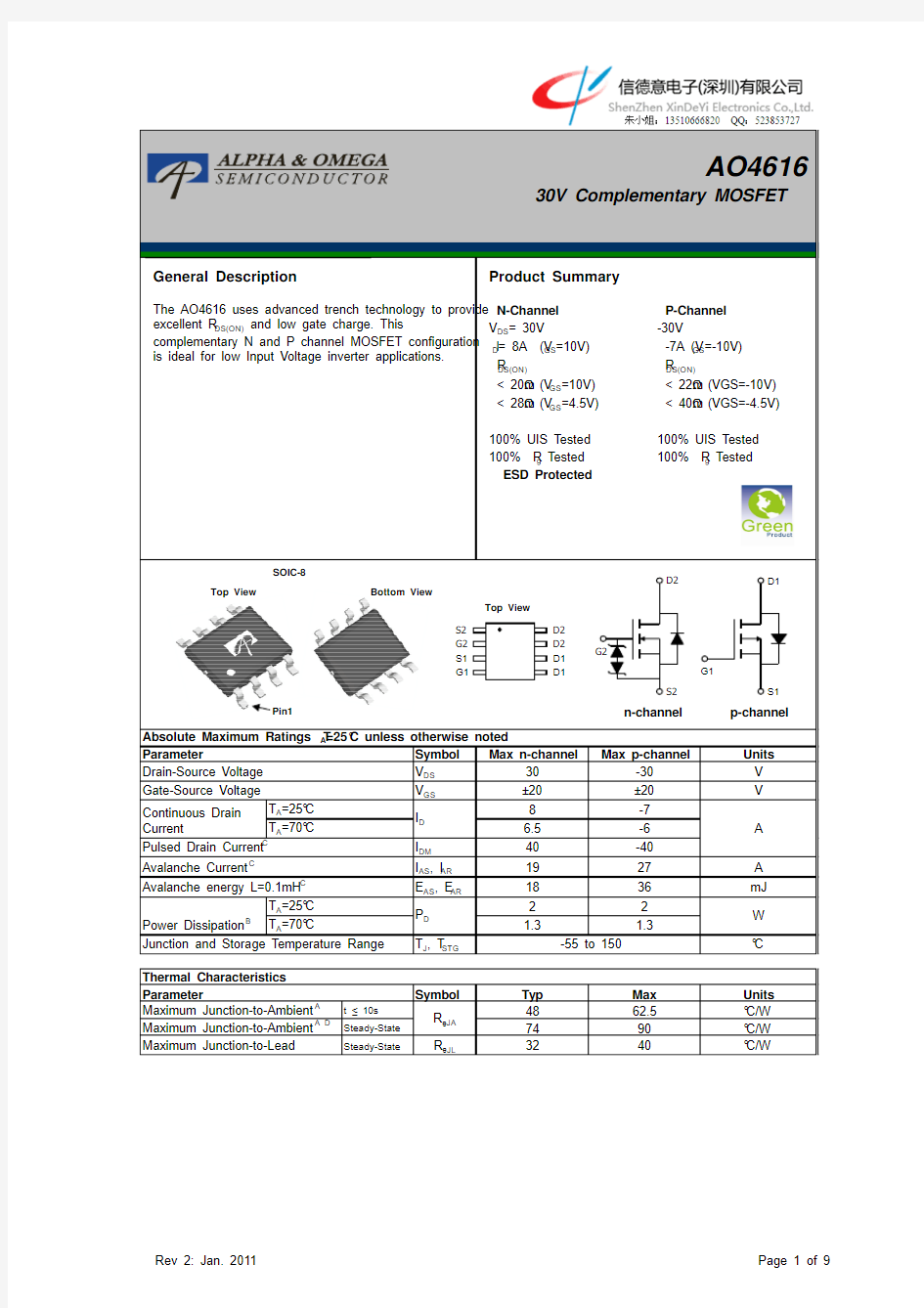
°C/W Maximum Junction-to-Ambient A D 32407490Top View Bottom View
Pin1
D1
S1
p-channel
Symbol
Min Typ Max Units BV DSS 30
V
V DS =30V, V GS =0V
1T J =55°
C 5I GSS 10
μA V GS(th)Gate Threshold Voltage 1.2 1.8
2.4V I D(ON)
40
A 16.520T J =125°
C 232819.528
m ?
g FS 30S V SD 0.75
1V I S
2.5
A C iss 600
740888pF C oss 77110145pF C rss 5082115pF R g
0.5 1.1 1.7?Q g (10V)12
1518nC Q g (4.5V)6
7.59
nC Q gs 2.5nC Q gd 3nC t D(on)5
ns t r 3.5ns t D(off)19ns t f 3.5
ns
t rr 6810ns Q rr
14
18
22
nC
THIS PRODUCT HAS BEEN DESIGNED AND QUALIFIED FOR THE CONSUMER MARKET. APPLICATIONS OR USES AS CRITICAL COMPONENTS IN LIFE SUPPORT DEVICES OR SYSTEMS ARE NOT AUTHORIZED. AOS DOES NOT ASSUME ANY LIABILITY ARISING OUT OF SUCH APPLICATIONS OR USES OF ITS PRODUCTS. AOS RESERVES THE RIGHT TO IMPROVE PRODUCT DESIGN,FUNCTIONS AND RELIABILITY WITHOUT NOTICE.
I F =8A, dI/dt=500A/μs
V GS =0V, V DS =15V, f=1MHz SWITCHING PARAMETERS N-Channel Electrical Characteristics (T J =25°C unless otherwise noted)STATIC PARAMETERS Parameter
Conditions Body Diode Reverse Recovery Time
Drain-Source Breakdown Voltage V GS =4.5V, I D =6A
I D =250μA, V GS =0V V GS =10V, V DS =5V V GS =10V, I D =8A
R DS(ON)Static Drain-Source On-Resistance
I DSS μA V DS =V GS I D =250μA V DS =0V, V GS =±16V Zero Gate Voltage Drain Current Gate-Body leakage current m ?On state drain current
I S =1A,V GS =0V
V DS =5V, I D =8A Forward Transconductance Diode Forward Voltage
Gate resistance
V GS =0V, V DS =0V, f=1MHz
Reverse Transfer Capacitance Turn-Off Fall Time
Total Gate Charge V GS =10V, V DS =15V, I D =8A
Gate Source Charge Gate Drain Charge Total Gate Charge Body Diode Reverse Recovery Charge I F =8A, dI/dt=500A/μs
Maximum Body-Diode Continuous Current
Input Capacitance Output Capacitance
Turn-On DelayTime DYNAMIC PARAMETERS Turn-On Rise Time Turn-Off DelayTime V GS =10V, V DS =15V, R L =1.8?,
R GEN =3?
A. The value of R θJA is measured with the device mounted on 1in 2
FR-4 board with 2oz. Copper, in a still air environment with T A =25°C. The value in any given application depends on the user's specific board design.B. The power dissipation P D is based on T J(MAX)=150°C, using ≤ 10s junction-to-ambient thermal resistance.C. Repetitive rating, pulse width limited by junction temperature T J(MAX)=150°C. Ratings are based on low frequency and duty cycles to keep initialT J =25°C.
D. The R θJA is the sum of the thermal impedence from junction to lead R θJL and lead to ambient.
E. The static characteristics in Figures 1 to 6 are obtained using <300μs pulses, duty cycle 0.5% max.
F. These curves are based on the junction-to-ambient thermal impedence which is measured with the device mounted on 1in 2 FR-4 board with 2oz. Copper, assuming a maximum junction temperature of T J(MAX)=150°C. The SOA curve provides a single pulse ratin g.
V GS (Volts)
Figure 2: Transfer Characteristics (Note E)
V DS (Volts)
Fig 1: On-Region Characteristics (Note E)
N-Channel: TYPICAL ELECTRICAL AND THERMAL CHARACTERISTICS
Q g (nC)
V G
S (V o l t s )
5
10
15202530
V DS (Volts)
Figure 8: Capacitance Characteristics C a p a c i t a n c e (p F )
Vds
Charge
Gate Charge Test Circuit & Waveform
Vdd
Resistive Switching Test Circuit & Waveforms
Vdd
Vds
Id
Vgs
BV I
Unclamped Inductive Switching (UIS) Test Circuit & Waveforms
AR
DSS
2
E = 1/2 LI Vdd AR AR
Symbol
Min Typ
Max
Units BV DSS -30
V
V DS =-30V, V GS =0V
-1
T J =55°C
-5I GSS 100
nA V GS(th)Gate Threshold Voltage -1.4-2.0-2.5
V I D(ON)-40
A
17.5
22T J =125°C
24.53327.540m ?g
FS 24S V SD -0.75
-1V I S
-2.5
A C iss 830
10401250pF C oss 125180235pF C rss 75125175pF R g
246?Q g (10V)15
1923nC Q g (4.5V)7.5
9.612
nC Q gs 3.6nC Q gd 4.6nC t D(on)10
ns t r 5.5ns t D(off)26ns t f 9ns
t rr 11.515ns Q rr
25
32.5
nC
THIS PRODUCT HAS BEEN DESIGNED AND QUALIFIED FOR THE CONSUMER MARKET. APPLICATIONS OR USES AS CRITICAL COMPONENTS IN LIFE SUPPORT DEVICES OR SYSTEMS ARE NOT AUTHORIZED. AOS DOES NOT ASSUME ANY LIABILITY ARISING OUT OF SUCH APPLICATIONS OR USES OF ITS PRODUCTS. AOS RESERVES THE RIGHT TO IMPROVE PRODUCT DESIGN,FUNCTIONS AND RELIABILITY WITHOUT NOTICE.
Body Diode Reverse Recovery Charge I F =-7A, dI/dt=500A/μs
Maximum Body-Diode Continuous Current
Input Capacitance Output Capacitance
Turn-On DelayTime DYNAMIC PARAMETERS Turn-On Rise Time Turn-Off DelayTime V GS =10V, V DS =-15V, R L =2.2?,
R GEN =3?
Gate resistance
V GS =0V, V DS =0V, f=1MHz
Turn-Off Fall Time
Total Gate Charge V GS =10V, V DS =-15V, I D =-7A
Gate Source Charge Gate Drain Charge Total Gate Charge V DS =V GS I D =-250μA R DS(ON)Static Drain-Source On-Resistance m ?Forward Transconductance I S =-1A,V GS =0V
V DS =-5V, I D =-7A V GS =-4.5V, I D =-3.5A Diode Forward Voltage
P-Channel Electrical Characteristics (T J =25°C unless otherwise noted)STATIC PARAMETERS Parameter
Conditions
I DSS μA V DS =0V, V GS =±20V
Zero Gate Voltage Drain Current Gate-Body leakage current Body Diode Reverse Recovery Time
Drain-Source Breakdown Voltage On state drain current
I D =-250μA, V GS =0V V GS =-10V, V DS =-5V V GS =-10V, I D =-7A
Reverse Transfer Capacitance I F =-7A, dI/dt=500A/μs
V GS =0V, V DS =-15V, f=1MHz SWITCHING PARAMETERS A. The value of R θJA is measured with the device mounted on 1in 2
FR-4 board with 2oz. Copper, in a still air environment with T A =25°C. The value in any given application depends on the user's specific board design.B. The power dissipation P D is based on T J(MAX)=150°C, using ≤ 10s junction-to-ambient thermal resistance.C. Repetitive rating, pulse width limited by junction temperature T J(MAX)=150°C. Ratings are based on low frequency and duty cycles to keep initialT J =25°C.
D. The R θJA is the sum of the thermal impedence from junction to lead R θJL and lead to ambient.
E. The static characteristics in Figures 1 to 6 are obtained using <300μs pulses, duty cycle 0.5% max.
F. These curves are based on the junction-to-ambient thermal impedence which is measured with the device mounted on 1in 2 FR-4 board with 2oz. Copper, assuming a maximum junction temperature of T J(MAX)=150°C. The SOA curve provides a single pulse ratin g.
P-Channel: TYPICAL ELECTRICAL AND THERMAL CHARACTERISTICS
-V GS (Volts)
Figure 2: Transfer Characteristics (Note E)
-I D (A )
-V DS (Volts)
Fig 1: On-Region Characteristics (Note E)
-I D (A )
P-Channel: TYPICAL ELECTRICAL AND THERMAL CHARACTERISTICS
5
101520
Q g (nC)
Figure 7: Gate-Charge Characteristics
-V G S (V o l t s )
05
10
15202530
-V DS (Volts)
Figure 8: Capacitance Characteristics C a p a c i t a n c e (p F )
Vds
Charge
Gate Charge Test Circuit & Waveform
Vdd
Vds
Id
Vgs
Unclamped Inductive Switching (UIS) Test Circuit & Waveforms
2
E = 1/2 LI AR AR
BV DSS
I AR
Vdd Vdd
Resistive Switching Test Circuit & Waveforms
90%
10%