EhLib 5 Developer’s guide 官方开发手册
- 格式:doc
- 大小:664.00 KB
- 文档页数:51
exoSip开发者手册exoSip 开发者手册1 扩展的eXosip协议栈1.1 如何初始化libeXosip2当使用eXosip时,你的首要任务是初始化eXosip上下文和libosip库(语法分析器和状态机)。
这是在使用libeXosip2之前一定要完成的。
includeint i;TRACE_INITIALIZE (6, stdout);i=eXosip_init();if (i!=0)return -1;//在特定的socket上监听i = eXosip_listen_addr (IPPROTO_UDP, NULL, port, AF_INET,0);if (i!=0){eXosip_quit();fprintf (stderr, "could not initialize transport layer\n");return -1;}…初始化之后就可以发送消息或者等待eXosip事件的到来…在前面的代码中,您学习了如何:初始化osip trace(用- DENABLE_TRACE编译此代码)初始化eXosip(和osip)堆栈为信号打开一个套接字(只有UDP要初始eXosip2)现在你要处理eXosip事件。
下面是一些来获得eXosip_event从在eXosip2堆栈的代码。
eXosip_event_t *je;for (;;){je = eXosip_event_wait (0, 50);eXosip_lock();eXosip_automatic_action ();eXosip_unlock();if (je == NULL)break;if (je->type == EXOSIP_CALL_NEW){........}else if (je->type == EXOSIP_CALL_ACK){........}else if (je->type == EXOSIP_CALL_ANSWERED) {........}else .............eXosip_event_free(je);你将为每个SIP消息的发送收到一个事件,每个事件包含。
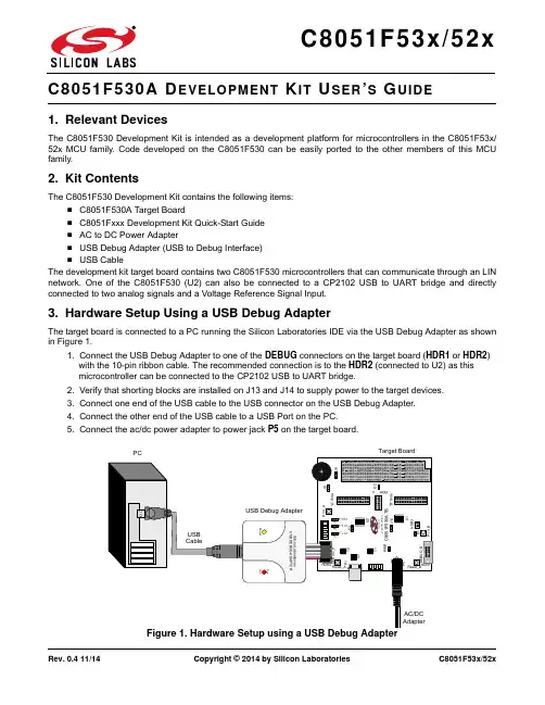
Rev. 0.4 11/14Copyright © 2014 by Silicon LaboratoriesC8051F53x/52xEVELOPMENT IT SER S UIDE1. Relevant DevicesThe C8051F530 Development Kit is intended as a development platform for microcontrollers in the C8051F53x/52x MCU family. Code developed on the C8051F530 can be easily ported to the other members of this MCU family.2. Kit ContentsThe C8051F530 Development Kit contains the following items:⏹ C8051F530A Target Board⏹ C8051Fxxx Development Kit Quick-Start Guide ⏹ AC to DC Power Adapter⏹ USB Debug Adapter (USB to Debug Interface)⏹ USB CableThe development kit target board contains two C8051F530 microcontrollers that can communicate through an LIN network. One of the C8051F530 (U2) can also be connected to a CP2102 USB to UART bridge and directly connected to two analog signals and a Voltage Reference Signal Input.3. Hardware Setup Using a USB Debug AdapterThe target board is connected to a PC running the Silicon Laboratories IDE via the USB Debug Adapter as shown in Figure 1.1. Connect the USB Debug Adapter to one of the DEBUG connectors on the target board (HDR1 or HDR2) with the 10-pin ribbon cable. The recommended connection is to the HDR2 (connected to U2) as this microcontroller can be connected to the CP2102 USB to UART bridge.2. Verify that shorting blocks are installed on J13 and J14 to supply power to the target devices.3. Connect one end of the USB cable to the USB connector on the USB Debug Adapter.4. Connect the other end of the USB cable to a USB Port on the PC.5. Connect the ac/dc power adapter to power jack P5 on the target board.D 1D 2H H D 4C8051F53x/52xNotes:e the Reset button in the IDE to reset the target when connected using a USB Debug Adapter.2. Remove power from the target board and the USB Debug Adapter before connecting or disconnecting theribbon cable from the target board. Connecting or disconnecting the cable when the devices have power can damage the device and/or the USB Debug Adapter.4. Software SetupSimplicity Studio greatly reduces development time and complexity with Silicon Labs EFM32 and 8051 MCU products by providing a high-powered IDE, tools for hardware configuration, and links to helpful resources, all in one place.Once Simplicity Studio is installed, the application itself can be used to install additional software and documentation components to aid in the development and evaluation process.Figure 2.Simplicity StudioThe following Simplicity Studio components are required for the C8051F530 Development Kit:⏹ 8051 Products Part Support ⏹ Simplicity Developer PlatformDownload and install Simplicity Studio from /8bit-software or /simplicity-studio .Once installed, run Simplicity Studio by selecting Start →Silicon Labs →Simplicity Studio →Simplicity Studio from the start menu or clicking the Simplicity Studio shortcut on the desktop. Follow the instructions to install the software and click Simplicity IDE to launch the IDE.The first time the project creation wizard runs, the Setup Environment wizard will guide the user through the process of configuring the build tools and SDK selection.C8051F53x/52xIn the Part Selection step of the wizard, select from the list of installed parts only the parts to be used during development. Choosing parts and families in this step affects the displayed or filtered parts in the later device selection menus. Choose the C8051F53x/52x family by checking the C8051F53x/52x check box. Modify the part selection at any time by accessing the Part Management dialog from the Window →Preferences →Simplicity Studio →Part Management menu item.Simplicity Studio can detect if certain toolchains are not activated. If the Licensing Helper is displayed after completing the Setup Environment wizard, follow the instructions to activate the toolchain.4.1. Running BlinkyEach project has its own source files, target configuration, SDK configuration, and build configurations such as the Debug and Release build configurations. The IDE can be used to manage multiple projects in a collection called a workspace. Workspace settings are applied globally to all projects within the workspace. This can include settings,such as key bindings, window preferences, and code style and formatting options. Project actions, such as build and debug, are context-sensitive. For example, the user must select a project in the Project Explorer view in order to build that project.To create a project based on the Blinky example, perform the following steps:1. Click the Software Examples tile from the Simplicity Studio home screen.2. In the Kit drop-down, select C8051F530A Development Kit ; in the Part drop-down, select C8051F530, and in the SDK drop-down, select the desired SDK. Click Next .3. Select Example , and click Next .4. Under C8051F530A Development Kit , select F52x-53x Blinky ; click Next , and click Finish .5. Click on the project in the Project Explorer , and click Build (the hammer icon in the top bar). Alternatively, go to Project →Build Project .6. Click Debug to download the project to the hardware and start a debug session.7. Press the Resume button to start the code running. The LED should blink.8. Press the Suspendbutton to stop the code.9. Press the Reset the devicebutton to reset the target MCU.10. Press the Disconnectbutton to return to the development perspective.4.2. Simplicity Studio HelpSimplicity Studio includes detailed help information and device documentation within the tool. The help containsdescriptions for each dialog window. To view the documentation for a dialog, click the question mark icon in the window:This will open a pane specific to the dialog with additional details.The documentation within the tool can also be viewed by going to Help →Help Contents or Help →Search .C8051F53x/52x4.3. CP210x USB to UART VCP Driver InstallationThe Target Board includes a Silicon Labs CP210x USB-to-UART Bridge Controller. Device drivers for the CP210x need to be installed before the PC software can communicate with the MCU through the UART interface.1. After opening Simplicity Studio for the first time, a dialog will prompt to install the CP210x drivers. Click Yes . The drivers can also be installed at any time by going to Help →Install Drivers →CP210x VCP USB Drivers .2. Accept the license agreement and follow the steps to install the driver on the system. The installer will let you know when your system is up to date. The driver files included in this installation have been certified by Microsoft.3. To complete the installation process, connect the included USB cable between the host computer and the USB connector (P4) on the Target Board. Windows will automatically finish the driver installation. Information windows will pop up from the taskbar to show the installation progress.4. If necessary, the driver files can be uninstalled by selecting Windows Driver Package—Silicon Laboratories...option in the Programs and Features window.4.4. Configuration Wizard 2The Configuration Wizard 2 is a code generation tool for all of the Silicon Laboratories devices. Code is generated through the use of dialog boxes for each of the device's peripherals.Figure 3.Configuration Wizard 2 UtilityThe Configuration Wizard 2 utility helps accelerate development by automatically generating initialization source code to configure and enable the on-chip resources needed by most design projects. In just a few steps, the wizard creates complete startup code for a specific Silicon Laboratories MCU. The program is configurable to provide the output in C or assembly language. For more information, refer to the Configuration Wizard documentation.Documentation and software is available on the kit CD and from the downloads web page: /mcudownloads .C8051F53x/52x 5. Target BoardThe C8051F52xA-53xA Development Kit includes a target board with two C8051F530A devices preinstalled for evaluation and preliminary software development. Numerous input/output (I/O) connections are provided to facilitate prototyping using the target board. Refer to Figure4 for the locations of the various I/O connectors.Table 1. Target Board Part SummaryPart DescriptionP5 Power connector (Accepts input from 7 to 15VDC unregulated power adapter.)PWR Red Power-on LED (D3)TB1 LINconnectorU55V Voltage RegulatorA SideJ2 28-pin Expansion I/O connector for U2HDR2 Debug connector for Debug Adapter Interface(D2)P1.3_A GreenLEDbuttonReset_A ResetbuttonP1.4_A PushR32Potentiometer for P1.2_AJ6, J8Connects R32 (potentiometer) to U2 and +5 VJ13Connects power to U2J11, J12Connects external crystal to U2 pins P0.7_A and P1.0_AJ3 Connects analog channel 1 to U2 P1.6_AJ4 Connects analog channel 2 to U2 P1.7_AJ5 Connects VREFIN to U2 P0.0_AconnectorTB2 AnaloginputHDR4 Connector block for serial port connection, Green LED, and push-buttonU3Silicon Laboratories CP2102 USB-to-UART BridgeP1 USB connector to serial interface (CP2102)USB ACTIVE Red USB Active LED (D4) (CP2102)T2 LINtransceiverU2 C8051F530A “A” SideC8051F53x/52x5.1. Target Board Shorting Blocks: Factory DefaultsThe C8051F530A target board comes from the factory with preinstalled shorting blocks on many headers. Figure 4shows the positions of the factory default shorting blocks.B SideJ1 26-pin Expansion I/O connector for U1HDR1Debug connector for Debug Adapter InterfaceP1.3_B Green LED (D1)Reset_B Reset button P1.4_B Push button J14Connects power to U1J9, J10Connects external crystal to U1 pins P0.7_B and P1.0_B HDR3Green LED and push-button connector blockT1 LIN transceiver U1C8051F530A “B” SideTable 1. Target Board Part SummaryPart DescriptionP1.4_BPWRUSB ACTIVE P1.3_AP1.3_B D2D1D4Pin 1C8051F53x/52x5.2. System Clock SourcesThe C8051F530A device installed on the target board features a calibrated programmable internal oscillator that is enabled as the system clock source on reset. After reset, the internal oscillator operates at a frequency of 191.4kHz (±0.5%) by default but may be configured by software to operate at other frequencies. Therefore, in many applications, an external oscillator is not required. However, if you wish to operate the C8051F530A device at a frequency not available with the internal oscillator, an external crystal may be used. Refer to the C8051F52x/ 52xA/53x/53xA data sheet for more information on configuring the system clock source.The target board is designed to facilitate the installation of external crystals. Install the crystals at the pads marked Y1 or Y2. Install a 10M resistor at R17 or R22, and install capacitors at C29 and C30 or C34 and C35 using values appropriate for the crystals selected. Headers J9, J10, J11, and J12 connect the external crystal pins to the general purpose I/O headers (J1 and J2). If the external crystal is in use, these headers should not be populated. Refer to the C8051F52x/52xA/53x/53xA data sheet for more information on the use of external oscillators.5.3. Switches and LEDsFour switches are provided on the target board.Switch RESET_A is connected to the RESET pin of the C8051F530A A-Side (U2).Switch RESET_B is connected to the RESET pin of the C8051F530A B-Side (U1).Pressing RESET_A or RESET_B puts the attached device into its hardware-reset state.Switches P1.4_A and P1.4_B are connected to the C8051F530A parts (U1 and U2) general purpose I/O (GPIO) pins through headers. Pressing P1.4_A or P1.4_B generates a logic low signal on the port pin of the respective microcontroller.Remove the shorting block from the header to disconnect P1.4_A or P1.4_B from the port pins. The port pin signals are also routed to pins on the J1 and J2 I/O connectors. See Table2 for the port pins and headers corresponding to each switch.Four LEDs are also provided on the target board. The red LED labeled PWR is used to indicate a power connection to the target board. The green LEDs labeled D1 and D2 are connected to the C8051F530A's GPIO pins through headers. Remove the shorting blocks from the headers to disconnect the LEDs from the port pins. The port pin signals are also routed to pins on the J1 and J2 I/O connectors. The red LED labeled USB ACTIVE is used to indicate that the CP2102 USB-to-UART bridge is properly connected to a PC and is ready for communication. See Table2 for the port pins and headers corresponding to each LED.A potentiometer (R32) is provided on the target board. Header J8 connects the potentiometer to +5V, and header J6 connects the potentiometer to the P1.2_A pin of the U2 A-Side C8051F530A microcontroller.Table 2. Target Board I/O DescriptionsDescription I/O HeaderReset_A U2-Reset noneReset_B U1-Reset noneP1.4_A U2-P1.4HDR4[3–4]P1.4_B U1-P1.4HDR3[3–4]Green LED D2U2-P1.3HDR4[1–2]Green LED D1U1-P1.3HDR3[1–2]Red LED D3PWR noneRed LED D4USB ACTIVE nonePotentiometer R32U2-P1.2J6, J8C8051F53x/52x5.4. Expansion I/O Connectors (J1, J2)The two Expansion I/O connectors J1 (26pins) and J2 (28pins) provide access to all signal pins of the C8051F530A devices. Pins for V DD, GND, 5V, Reset, Vbat, LIN, 3.3V, and VREFIN are also available. A small through-hole prototyping area is also provided.All I/O signals routed to connectors J1 and J2 are also routed to through-hole connection points between J1 and J2 and the prototyping area (see Figure4). Each connection point is labeled indicating the signal available at the connection point. Table3 lists the pin descriptions for J1 and J2.Table 3. Pin Descriptions for J1 and J2J1J2Pin #Description Pin #Description Pin #Description Pin #Description 1P0.0_B14P1.5_B1P0.0_A15P1.6_A 2P0.1_B15P1.6_B2P0.1_A16P1.7_A 3P0.2_B16P1.7_B3P0.2_A17+5V4P0.3_B17+5V4P0.3_A18RST/C2CLK_A 5P0.4_B18RST/C2CLK_B5P0.4_A19VBAT 6P0.5_B19VBAT6P0.5_A20LIN7P0.6_B20LIN7P0.6_A21VREFIN 8P0.7_B21NC8P0.7_A22VREGOUT_A 9P1.0_B22VREGOUT_B9P1.0_A23+3.3V 10P1.1_B23NC10P1.1_A24NC11P1.2_B24NC11P1.2_A25NC12P1.3_B25GND12P1.3_A26NC13P1.4_B26GND13P1.4_A27GND14P1.5_A28GND5.5. Target Board DEBUG Interface (HDR1, HDR2)The DEBUG connectors (HDR1 and HDR2) provide access to the DEBUG (C2) pins of the C8051F530A parts. They are used to connect the USB Debug Adapter to the target board for in-circuit debugging and Flash programming. Table4 shows the DEBUG pin definitions.Table 4. DEBUG Connector Pin DescriptionsPin #Description1+3VD(+3.3VDC)2, 3, 9GND (Ground)4C2D5RST (Reset)6P0.67C2CK8Not Connected10USB PowerC8051F53x/52x5.6. USB to Serial Connector (P1, HDR4)A USB-to-Serial bridge interface is provided. A B-type USB connector (P1), a CP2102, and related circuits are provided to facilitate the serial connection between a PC and the U2 A-Side C8051F530A microcontroller on the target board. The RX, TX, CTS, and RTS signals of the UART side of the Bridge (CP2102) may be connected to the microcontroller by installing shorting blocks on HDR4 as shown in Table5.Table 5. UART ConnectionsHDR3Connection Signals5–6P0.4_A to TX_A7–8P0.5_A to RX_A9–10P1.1_A to RTS_A11–12P1.2_A to CTS_AThe BUS-Powered CP2102 uses the 5V provided by the USB interface.5.7. Analog I/O (TB2, J3, J4, J5)The Analog connector block (TB2) and headers J3, J4, and J5 provide Analog inputs to the C8051F530A (U2) as shown in Table6. Headers J3, J4, and J5 connect the inputs from the Analog connector to the microcontroller pins.Table 6. Analog I/O ConnectionsTB2Signal Connection I/O Shorting Block Vrefin External Reference Input or Internal Reference Output P0.0_A J5CH1Analog Input 1P1.6_A_MC J3CH2Analog Input 1P1.7_A_MC J4GND Ground GND—5.8. Power Supply Options (P5, TB1, J13, J14)The target board provides two options of power supply. The first option is to use the provided 9V power supply attached to the P5 connector. The second option is to use an external 12V (7.5V minimum) connected to the TB1 terminal block (pins 1 and 3).Headers J13 and J14 connect the +5V power supply to the VREGIN pins on U1 and U2. These headers can be populated to supply power directly or depopulated to measure the operating current drawn by the corresponding C8051F530A device.C8051F53x/52x5.9. LIN Connectivity (TB1)The C8051F530A Target Board has two C8051F530A devices (U1 and U2) and two LIN transceivers (T1 and T2) to provide LIN connectivity on the target board. These devices can also be interfaced to another LIN bus using the TB1 terminal block.Table 7. LIN ConnectionsTB1Signal Connection+12V Supplies 12V (7.5V minimum) to the target board. This can be connected to the power supply of another LIN bus or any external supply.LIN Connects the 12V LIN bus signal to the T1 and T2 LIN transceivers.GND GroundC8051F53x/52x6. SchematicsF i g u r e 5.C 8051F 530A T a r g e t B o a r d S c h e m a t i c (1 o f 3)C8051F53x/52xF i g u r e 6.C 8051F 530A T a r g e t B o a r d S c h e m a t i c (2 o f 3)C8051F53x/52xF i g u r e 7.C 8051F 530A T a r g e t B o a r d S c h e m a t i c (3 o f 3)C8051F53x/52xD OCUMENT C HANGE L IST Revision 0.2 to Revision 0.3⏹Updated for C8051F530A TB.⏹Added "LIN Connectivity (TB1)‚" on page 10. Revision 0.3 to Revision 0.4⏹Updated "Software Setup‚" on page 2.DisclaimerSilicon Laboratories intends to provide customers with the latest, accurate, and in-depth documentation of all peripherals and modules available for system and software implementers using or intending to use the Silicon Laboratories products. Characterization data, available modules and peripherals, memory sizes and memory addresses refer to each specific device, and "Typical" parameters provided can and do vary in different applications. Application examples described herein are for illustrative purposes only. Silicon Laboratories reserves the right to make changes without further notice and limitation to product information, specifications, and descriptions herein, and does not give warranties as to the accuracy or completeness of the included information. Silicon Laboratories shall have no liability for the consequences of use of the information supplied herein. This document does not imply or express copyright licenses granted hereunder to design or fabricate any integrated circuits. The products must not be used within any Life Support System without the specific written consent of Silicon Laboratories. A "Life Support System" is any product or system intended to support or sustain life and/or health, which, if it fails, can be reasonably expected to result in significant personal injury or death. Silicon Laboratories products are generally not intended for military applications. Silicon Laboratories products shall under no circumstances be used in weapons of mass destruction including (but not limited to) nuclear, biological or chemical weapons, or missiles capable of delivering such weapons.Trademark InformationSilicon Laboratories Inc., Silicon Laboratories, Silicon Labs, SiLabs and the Silicon Labs logo, CMEMS®, EFM, EFM32, EFR, Energy Micro, Energy Micro logo and combinations thereof, "the world’s most energy friendly microcontrollers", Ember®, EZLink®, EZMac®, EZRadio®, EZRadioPRO®, DSPLL®, ISOmodem ®, Precision32®, ProSLIC®, SiPHY®, USBXpress® and others are trademarks or registered trademarks of Silicon Laboratories Inc. ARM, CORTEX, Cortex-M3 and THUMB are trademarks or registered trademarks of ARM Holdings. Keil is a registered trademark of ARM Limited. All other products or brand names mentioned herein are trademarks of their respective holders.Silicon Laboratories Inc.400 West Cesar Chavez Austin, TX 78701USAIoT Portfolio /IoTSW/HW/simplicityQuality/qualitySupport and Community。

嵌入式系统原理与应用实验栗华编着山东大学信息科学与工程学院二零一四年三月目录第一章实验硬件平台1.1北京博创UP-TECH三合一实验箱简介本实验指导书所依赖的硬件平台为北京博创兴盛科技有限公司生产的一种ARM9/Xscale经典三核心教学科研平台(型号:UP-TECHS2410/S2440/P270),本平台兼容PXA270核心CPU及S3C2410、S2440核心CPU的全部功能,是北京博创多年来嵌入式教学产品开发经验的结晶。
这里选配的是S3C2440核心板。
图1-1UP-CUP三合一实验箱外观应用案例:※支持Linux、WinCE、Vxworks、μC/OS-Ⅱ4套操作系统;※核心板可更换,同时拥有ARM9(S3C2410和S3C2440)和XScale(PXA270);※中国电子学会嵌入式工程师认证考试和师资培训指定平台;硬件资源:软件资源结构说明图1-2UP-TECH三合一实验箱实物结构图1-2UP-TECH三合一实验箱框图结构图1-3UP-TECH三合一实验箱框图结构版图1.2跳线设置参考说明:◆PCB上所有“EXPORT”丝印字符表示168Pin扩展槽◆JP1401RESET-SEL:设置复位电路,位置JTAG20插座下方。
1-2:ICE的ICE-TRST复位信号可以控制系统复位信号RESET。
2-3:ICE的ICE-TRST复位信号不可以控制系统复位信号RESET。
◆JP1402JTAGSEL:选择JTAG电路,位置JTAG20插座下方。
1-2:使能板载的UP-LINKJTAG电路。
2-3:使用外部的JTAG电缆或者ARMICE仿真器。
◆JP1103TXD1-SEL◆JP1104RXD1-SEL:UART1选择扩展槽或者RS232的DB9插座。
1-2:UART1连接RS232-1,从DB9串口插座输出。
2-3:UART1连接到扩展槽。
◆JP1101TXD2-SEL◆JP1102RXD2-SEL:UART2选择跳线,分别为RS485、IrDA、扩展槽1-2:UART2连接到RS485总线上。

OBT-BSP-Rtems 应用开发手册V 2.0珠海欧比特宇航科技股份有限公司2011年6月26日目录1RTEMS概况 (1)2OBT-BSP-RTEMS说明 (2)2.1PROMCOREL文件 (4)2.2BOOT_CARD函数 (5)2.3BSP_START函数 (6)3RTEMS开发环境的搭建 (7)3.1RCC简介 (7)3.2RCC的安装 (7)3.3RCC的目录结构 (8)4RTEMS LIB开发 (9)4.1目录结构 (9)4.2硬件相关源代码 (11)4.3编译RTEMS LIB库 (11)5RTEMS应用程序开发 (12)5.1示例程序源码分析 (12)5.2编译RTEMS应用程序 (19)5.3在S698平台上运行RTEMS应用程序 (19)1RTEMS概况RTEMS (Real-Time Executive for Multiprocessor Systems)是一个支持多处理器系统的高性能实时嵌入式操作系统,主要应用于嵌入式军事应用领域。
它主要有以下特点:具备多任务处理能力;适用于同类或异类多处理器系统;事件驱动、基于优先级的抢占式调度;可选的单调速率调度机制;任务间通讯和同步;优先级继承;中断响应管理;动态内存分配;高级用户配置。
RTEMS 由ADA和C共同实现,它支持Intel X86、Motorola MC68K、MIPS、PowerPC、SPARC等主流处理器。
RTEMS完全支持个人微处理器家族或特殊功能硬件的特性,允许系统开发人员高度自由的定制和扩展它的特征。
易移植性是RTEMS开发中最主要的因素,它对硬件的依赖性小,实时应用可以很容易的移植到任何其它的处理器上。
采用RTEMS的实时系统,其功能升级完全不受特定的微处理器结构约束。
RTEMS支持多处理器系统,包括同类处理器和异类处理器。
它的内核能自动补偿处理器之间的结构差异(字节交换等),这使得一个处理器与其不同类的处理器交互变得简单,而不需要重新为其设计系统。

DKBLEUSER GUIDE Monday, 19 May 2014Version 1.0VERSION HISTORYTABLE OF CONTENTS1Design Overview (5)1.1PIO Connections in the Carriers (7)1.2Important Notes about the Differences between the Module Carriers (7)1.2.1Why the External Flash Chip Doesn’t Work With BLE121LR Carrier? (9)1.2.2Minimizing the Current Consumption (9)1.3Sensors, display and USB to UART converter (9)2Getting Started With DKBLE (10)2.1Using the On-Board Debugger to Program the Carriers (10)2.2Using the On-Board Debugger to Program External BLE Devices (11)2.3Using the Analog Comparator of BLExxx modules (11)3Measuring Current Consumption (12)4Schematics and Assembly Drawing (14)5WEEE Compliance (20)6Contact Information (20)1 Design OverviewBLE Development Kit, DKBLE, is targeted for engineers evaluating Bluetooth Smart modules BLE112, BLE113 and BLE121LR. DKBLE is platform containing various switchable peripherals for creating and testing several different applications utilizing Bluegiga Bluetooth Smart modules. The modules are assembled on a carriers boards and DKBLE contains a header type of interface for plugging in the module carriers. Thus each module can be tested and compared with each other on the same platform. DKBLE contains:To measure the DC current drawn from the battery, connect current meter here.To measure the DC current drawn from the USB, connect current meter here.To measure the DC current drawn by the module alone, connect current meter here.To measure the peak current drawn by the module alone, connect oscilloscope here.Interface for the module carrier boards.Plug the carrier board to this connector.Signal test points. All the signals and interfaces of this boardare exposed here. The silk screen describes the functions of this board. To see which module IO is connected to particular function, see the silk screen of the module carrier.Output of the on-board cc-debugger.To program an external BLExxx device,connect the debug interface of the device here.To program the module carrier, switch to ”MODULE”To program an external BLExxx device,switch to ”OUTPUT”Select power from the battery or from the USB.UART, USB and CC-Debugger interfaces.The board can be powered from any of these USB lines.Potentiometer to test the internal ADC of BLExxx modules.Switches to connect and enable / disconnect and disable the onboard peripherals.Reset the module carrier.Module peak current measurement on/off. To save in current consumption turn off when not used.Push buttons to the IO’s of the moduleP h y s i c a l D i m e n s i o n s o 1L R0 Figure 3: BLE121LR module carrier1.1 PIO Connections in the Carriers*) Connect using a shorting link in the carrierTable 1: PIO connections in the carriers1.2 Important Notes about the Differences between the Module CarriersIn BLE121LR the PIOs P1_0 and P1_1 are reserved for the internal front end control of the module. Also P1_7 is reserved for this purpose and in case of BLE121LR it can only be used as an output controlling the external DCDC. Thus in BLE121LR P1_7 is named as DCDC CNTRL.The important differences between the carriers are shown in the Figure 4 (BLE112 and BLE113 carriers) and Figure 5 (BLE121LR carrier).1.2.1 Why the External Flash Chip Doesn’t Work With BLE121LR Carrier?The external flash chip is powered with one of the IO’s of the module. In BLE121LR Carrier the Flash supply is connected to an IO with 4 mA current driving capability where as in BLE112 and BLE113 Carrier it is connected to an IO with 20 mA current driving capability. Thus BLE121LR carrier is not able to power the flash and using the flash with BLE121LR carrier is not possible in DKBLE.1.2.2 Minimizing the Current ConsumptionIn all Carriers pin P1_4 is externally pulled down by the pull-down resistor in DKBLE. The purpose of this resistor is to avoid leakage when using the display. Note that any PIO’s configured as peripherals do not have internal pull-down or pull-up capability and thus, when left floating, they will require external pull-down resistor.For this reason port P1 can’t be configured to have internal pull-ups (the default settingof the module) but the port P1 must be pulled low in the HW configuration file.In BLE121LR carrier also pin P0_7 is externally pulled down by the pull-down resistor in DKBLE.For these reasons both ports P1 and P2 must be pulled low in the HW configuration file. The PIO used for the display RS (Register Select) signal has an external pull-down resistor in DKBLE (Note that P1_0 and P1_1 require external pull-up or pull-down when configured as input).For these reasons the PIO used for the RS signal must be driven low when the notwriting to the display.1.3 Sensors, display and USB to UART converterTable 2: Sensors, display, external flash and USB to UART converter in DKBLE2 Getting Started With DKBLEBy default the modules delivered with the DKBLE have demonstration FW which prints the temperature to the display and starts automatically advertising. Several example applications are provided with the SDK package downloadable in the Bluegiga web pages.To get started with the example applications navigate to→Products → Bluetooth 4.0 ModulesSelect the module of your choice and then navigate toDocument ation and Software → Software Releases → Bluetooth Smart Software and SDKDownload and install the package. After successful installation the tools can be found from the start menu.Figure 6: Bluegiga tools and examples in the Windows start menu2.1 Using the On-Board Debugger to Program the CarriersTo program the module in the carrier, connect the debugger with USB to a PC as shown in the Figure 7. Launch the BLE SW Update Tool. Browse to select the project file for the right module carrier, and then click “update”. After successful programming, the background of the BLE SW Update Tool turns into green (Figure 8).”module”“reset debugger”Figure 7: Using the on-board debugger to program the carrierFigure 8: Using the BLE Update Tool2.2 Using the On-Board Debugger to Program External BLE DevicesFigure 9: Using the on-board debugger to program external BLE devices2.3 Using the Analog Comparator of BLExxx modulesSwitch power to ”USB” and the debugger to ”OUTPUT ”Connect the ribbon cable from the “DEBUGGER OUTPUT” to the programming port of the target deviceFigure 10: Measuring the current consumptionThe peak current consumption of the module is measured over 3 ohm resistor using an instrumentation amplifier with a gain of 10. The instrumentation amplifier is powered from USB 5V line and the DC bias is from the 3V3 LDO. Because the amplifier is powered from the USB VBUS, it can’t be use d unless USB is connected. If USB is not connected then the instrumentation amplifier must be turned off and by-passed using the switch labeled “CURRENT MEAS OFF<->ON to avoid excessive leakage current into the input of the amplifier.NOTE: Peak current measurement is not possible when the external DCDC is used3RA=10-+RefFigure 11: TX current measurement amplifierTo measure the peak TX current consumption of the module, connect a coaxial cable to the BNC connector in the board and to an oscilloscope. Set the oscilloscope ∙Coupling: DC∙Vertical scale 500 mV/DIV ∙Horizontal scale: 200 µs/DIV ∙Level: 2.5 V ∙Offset: -2.0 V∙Trigger: Normal, falling edgeThe instrumentation amplifier inverts the signal. The current consumption is calculated byΩ-=303.3Vo V I NOTE: Because of the limited common mode input range of the instrumentation amplifier the peakcurrent can only be measured when powering the module from USB.4 Schematics and Assembly DrawingFigure 12: BLE113 Evaluation Board Schematic (1/6)Silicon LabsPage 14 of 20Silicon LabsPage 15 of 20Figure 13: BLE113 Evaluation Board Schematic (2/6)Figure 14: BLE113 Development Board Schematic (3/6)Silicon LabsPage 16 of 20Silicon LabsPage 17 of 20Figure 15: BLE113 Development Board Schematic (4/6)Figure 16: BLE113 Development Board Schematic (5/6)Silicon LabsPage 18 of 20Silicon LabsPage 19 of 20Figure 17: BLE113 Development Board Schematic (6/6)Silicon Laboratories Inc.400 West Cesar Chavez Austin, TX 78701USASimplicity StudioOne-click access to MCU and wireless tools, documentation, software, source code libraries & more. Available for Windows, Mac and Linux!IoT Portfolio /IoTSW/HW/simplicityQuality/qualitySupport and CommunityDisclaimerSilicon Laboratories intends to provide customers with the latest, accurate, and in-depth documentation of all peripherals and modules available for system and software implementers using or intending to use the Silicon Laboratories products. Characterization data, available modules and peripherals, memory sizes and memory addresses refer to each specific device, and "Typical" parameters provided can and do vary in different applications. Application examples described herein are for illustrative purposes only. Silicon Laboratories reserves the right to make changes without further notice and limitation to product information, specifications, and descriptions herein, and does not give warranties as to the accuracy or completeness of the included information. Silicon Laboratories shall have no liability for the consequences of use of the information supplied herein. This document does not imply or express copyright licenses granted hereunder to design or fabricate any integrated circuits. The products are not designed or authorized to be used within any Life Support System without the specific written consent of Silicon Laboratories. A "Life Support System" is any product or system intended to support or sustain life and/or health, which, if it fails, can be reasonably expected to result in significant personal injury or death. Silicon Laboratories products are not designed or authorized for military applications. Silicon Laboratories products shall under no circumstances be used in weapons of mass destruction including (but not limited to) nuclear, biological or chemical weapons, or missiles capable of delivering such weapons.Trademark InformationSilicon Laboratories Inc.® , Silicon Laboratories®, Silicon Labs®, SiLabs® and the Silicon Labs logo®, Bluegiga®, Bluegiga Logo®, Clockbuilder®, CMEMS®, DSPLL®, EFM®, EFM32®, EFR, Ember®, Energy Micro, Energy Micro logo and combinations thereof, "the world’s most energy friendly microcontrollers", Ember®, EZLink®, EZRadio®, EZRadioPRO®, Gecko®, ISOmodem®, Precision32®, ProSLIC®, Simplicity Studio®, SiPHY®, Telegesis, the Telegesis Logo®, USBXpress® and others are trademarks or registered trademarks of Silicon Laborato-ries Inc. ARM, CORTEX, Cortex-M3 and THUMB are trademarks or registered trademarks of ARM Holdings. Keil is a registered trademark of ARM Limited. All other products or brand names mentioned herein are trademarks of their respective holders.。

/CN/view/zh/109485822C o p y r i g h t S i e m e n s A G C o p y r i g h t y e a r A l l r i g h t s r e s e r v e dContentsSINAMICS G110 G120系列驱动产品文档列表............................................................ 1 1. 概括 ............................................................................................................................. 3 2. 样本列表 ..................................................................................................................... 3 3. 手册列表 ..................................................................................................................... 3 4. 常问问题 ..................................................................................................................... 7 5. 操作入门 ................................................................................................................... 38 6. 视频列表 ................................................................................................................... 41 7. 软件列表 ................................................................................................................... 45 8. GSD 列表 .................................................................................................................... 47 9.附录网址 (47)C o p y r i g h t S i e m e n s A G C o p y r i g h t y e a r A l l r i g h t s r e s e r v e d1. 概括本文主要总结了SINAMICS G110,G120驱动产品的文档列表,供客户方便查找。

EC系列小型可编程控制器应用问答集锦资料版本归档时间2007-05-18BOM编码艾默生网络能源有限公司为客户提供全方位的技术支持,用户可与就近的艾默生网络能源有限公司办事处或客户服务中心联系,也可直接与公司总部联系。
艾默生网络能源有限公司版权所有,保留一切权利。
内容如有改动,恕不另行通知。
艾默生网络能源有限公司地址:深圳市南山区科技工业园科发路一号邮编:518057公司网址:技术服务热线:800-8206510手机及未开通800地区:客户服务投诉热线:0E-mail前言目标读者本书适用于自动化技术人员,帮助他们解决在使用艾默生可编程控制器(以下简称PLC)中出现的问题,为广大艾默生PLC用户编程、系统设计和系统调试提供参考。
手册内容该手册通过问答的形式帮助用户解决在使用艾默生PLC时可能出现的产品应用问题、与周边设备连接问题、行业应用问题等。
回答中涉及的例子程序,发布在艾默生网络能源有限公司主页上。
阅读本手册的同时也可以参考阅读以下手册:■《EC系列小型可编程控制器编程手册》■《EC10 系列可编程控制器用户手册》■《EC20 系列可编程控制器用户手册》■《ControStar 编程软件用户手册》目录第一章硬件相关问题 ..................................................................... 错误!未定义书签。
PLC输出点控制交流接触器,应注意些什么?............................................ 错误!未定义书签。
EC系列小型PLC的输出触点容量是多少? .............................................. 错误!未定义书签。
PLC出现误动作怎么办? ............................................................. 错误!未定义书签。

Intel开发者⼿册第⼆卷指令集⼿册第2章指令格式这⼀章详细描述所有Intel 64和IA-32处理器指令格式.保护模式指令,实地址模式以及虚拟8086模式指令格式将在2.1节描述.IA-32e模式及其⼦模式指令格式将在2.2节描述.2.1 实模式,保护模式,以及虚拟8086模式指令格式Intel-64和IA-32架构指令编码是图2-1所⽰格式的⼦集.⼀条指令包括可选的指令前缀(顺序任意),主操作码(最多3字节),由ModR/M和SIB字节(可选) 组成的地址格式描述符(如果需要的话),偏移量(可选)以及⽴即数(可选).图 2-1. Intel 64 和 IA-32 架构指令格式2.1.1 指令前缀指令前缀分为四组,每⼀组包含⼀些允许的前缀码.对于任何指令,前缀可以从这四组(组1,2,3,4)⾥的挑选,并且它们不区分次序.组1—锁定和重复前缀:Vol. 2A 2-1指令格式F0H - LOCKF2H - REPNE/REPNZ,仅⽤于串操作和I/O指令,也可被⽤作某些指令的强制性前缀F3H - REP或REPE/REPZ,仅⽤于串操作和I/O指令,也可被⽤作某些指令的强制性前缀组2—段重载前缀:2EH—CS 段重载(⽤于任意分⽀指令时保留 )36H—SS 段重载(⽤于任意分⽀指令时保留 )3EH—DS 段重载(⽤于任意分⽀指令时保留 )26H—ES 段重载(⽤于任意分⽀指令时保留 )64H—FS 段重载(⽤于任意分⽀指令时保留 )65H—GS 段重载(⽤于任意分⽀指令时保留 )—分⽀提⽰:2EH—分⽀不被接受(仅⽤于Jcc指令中)3EH—分⽀被接受(仅⽤于Jcc指令中)组366H—操作数⼤⼩重载前缀,也可被⽤作某些指令的强制性前缀.组467H—地址尺⼨重载前缀LOCK前缀(F0H)在多处理器环境下强制执⾏独占共享内存操作.详见《Instruction Set Reference, A-M》第三章"LOCK –断⾔LOCK#信号前缀".重复前缀(F2H,F3H)将会重复操作字符串的每⼀个元素.只有MOVS,CMPS,SCAS,LODS,STOS,INS,OUTS等字符串操作或I/O指令才能使⽤这些前缀. 对Intel 64 或 IA-32 其他指令使⽤重复前缀和/或未定义的操作码是被保留的,将会引起不可预知的⾏为.某些指令可能使⽤F2H,F3H作为强制性前缀来表⽰特定的功能.强制性前缀应当位于其他可选的前缀之后(例外的情形请查看第2.2.1节,‖REX前缀‖)2-2 Vol. 2A指令格式分⽀提⽰前缀(2EH,3EH)允许程序给处理器⼀个最有可能的执⾏分⽀提⽰.这些前缀只能⽤于条件指令(Jcc).在Intel 64 或 IA-32其他指令中使⽤分⽀预测前缀或者未定义的操作码是被保留的,将引起不可预知的⾏为.操作数⼤⼩重载前缀允许程序在16位和32位操作数⼤⼩间切换.它们中任⼀个都可以是默认值,⽽使⽤这个前缀则选择⾮默认值.某些SSE2/SSE3/SSSE3/SSE4和使⽤3字节操作码的指令可能使⽤66H作为强制性前缀来表⽰特定的功能. 强制性前缀应当位于其他可选的前缀之后(例外的情形请查看第2.2.1节,‖REX前缀‖) . 66H前缀的其他⽤法是被保留的, 将引起不可预知的⾏为.地址尺⼨重载前缀(67H)允许程序在16位和32位地址间切换.它们中的任何⼀个都可以是默认值,使⽤这个前缀选择⾮默认值.当指令中的操作数不在内存中,使⽤这个前缀或未定义的操作码时,操作被保留,可能引起不可预知的⾏为.2.1.2 操作码主操作码长度为1,2或3字节. ModR/M可能编码附加的3位操作码. 主操作码中定义了⼀些更⼩的域.这些域定义了操作⽅向,偏移⼤⼩,寄存器编码,条件代码,或符号扩充.指令使⽤的域因操作码的类别⽽不同.双字节通⽤和SIMD指令操作码由下⾯部分组成:转义码(0FH),加上第⼆个操作码字节,或者⼀个强制性前缀(66H,F2H,或F3H), 转义码(0FH),第⼆个操作码字节(和上⾯⼀样)例如,CVTDQ2PD由下⾯的⼆进制序列组成:F3 0F E6 .第⼀个字节是⼀个SSE/SSE2/SSE3指令的强制性前缀(不被视为重复前缀).三字节通⽤和SIMD指令操作码由下⾯部分组成:转义码(0FH),加上另外2个操作码字节,或者⼀个强制性前缀(66H,F2H,或F3H), 转义码(0FH),另外2个操作码字节(和上⾯⼀样)⽐如,XMM寄存器指令PHADDW由下⾯的⼆进制序列组成:66 0F 38 01.第⼀个字节即强制性前缀.有效的操作码在附录A和附录B中被定义.Vol. 2A 2-3指令格式2.1.3 ModR/M 和 SIB 字节许多涉及内存操作数的指令都有⼀个紧挨着主操作码的寻址格式说明字节(叫做ModR/M字节),ModR/M字节包含3个域信息:mod域与r/m域组成32个可能的值:8个寄存器和24个寻址模式.reg/opcode域确定寄存器号或者附加的3位操作码.reg/opcode域的⽤途由主操作码确定.r/m域确定⼀个寄存器为操作数或者和mod域⼀起编码寻址模式.有时候有些指令使⽤特定的mod域和r/m域组合来表⽰操作码信息.某些ModR/M字节编码需要第⼆寻址字节(SIB).基址+索引或者⽐例+索引形式的32位寻址需要SIB字节.SIB字节包括下列域: scale 域指定⽐例因⼦.index域指定索引寄存器号.base 域指定基址寄存器号.ModR/M和SIB编码详见第2.1.5节.2.1.4 偏移量和⽴即数字节某些地址构成包含ModR/M以及紧随ModR/M其后的偏移量(或者是SIB字节).如果需要偏移量,它可以是1,2,或者4字节.若指令指定⼀个⽴即操作数,该操作数总是在偏移量之后,⽴即操作数可以为1,2,4字节. 2.1.5 ModR/M和SIB字节寻址模式编码表2-1⾄表2-3列出了ModR/M和SIB字节和寻址模式的对应情况:表2-1列出的是16位地址模式的情形,⽽表2-2则是32位的情况,表2-3则是由SIB字节指定的32位地址的情况.在附录B中列出了当ModR/M的reg/opcode域表现为操作码扩展时的编码情况.在表2-1和2-2中,指定了由Mod域和R/M域组合的32种有效地址形式,其中前24个是内存操作数,后8个(mod=11B)是供通⽤寄存器,MMX以及XMM寄存器使⽤.2-4 Vol. 2A指令格式表2-1和2-2中的Mod和R/M列给出了第⼀列对应有效地址时Mod和R/M的值.例如:Mod=11B,R/M=000B,该⾏确定通⽤寄存器EAX,AX或AL,MMX寄存器MM0,或者XMM寄存器XMM0.最终使⽤的寄存器由操作码字节以及操作数尺⼨属性决定.现在看看表2-1或2-2的第7⾏(―REG=‖),当需要指定第⼆操作数时,该⾏指定Reg/Opcode 域的⽤途,该操作数必须为通⽤寄存器或者MMX,XMM寄存器,第⼀⾄五⾏为对应的寄存器,同样的,最终使⽤的寄存器由操作码字节以及操作数尺⼨属性决定.若指令不需要第⼆操作数,Reg/Opcode可能被⽤作操作码扩展,即第六⾏‖/digit(Opcode)‖所指,以⼗进制数的形式表⽰.表2-1和2-2的主体(即‖ ModR/M值 (⼗六进制)‖)是⼀个32*8的矩阵,囊括了ModR/M的256个可能值.由位3-5索引列,位0-2和6,7索引列.下图演⽰了表中的⼀个值的解析.图 2-2. ModR/M (C8H) 值的解析Vol. 2A 2-5指令格式注:1. BP作为索引默认以SS为段寄存器,其他的寻址⽅式默认以DS段寄存器.2. “disp16”记号表⽰ModR/M 后跟随⼀个16位的偏移量,该偏移量被加⾄有效地址.3. “disp8”记号表⽰ModR/M 后跟随⼀个8位的偏移量,该偏移量将被符号扩展,然后被加⾄有效地址.2-6 Vol. 2A指令格式注:1. “[--][--]”记号表⽰ModR/M 后跟随有⼀个SIB字节.2. “disp32”记号表⽰ModR/M(或者SIB,如果出现的话) 后跟随⼀个32位的偏移量,该偏移量被加⾄有效地址.3. “disp8”记号表⽰ModR/M(或者SIB,如果出现的话) 后跟随⼀个8位的偏移量,该偏移量将被符号扩展,然后被加⾄有效地址.表2-3囊括了SIB 的256个可能值(⼗六进制形式) . 可以作为基的通⽤寄存器通过表的上部列出,也列出了相应的base域值. 表的主体的每⾏列出了索引(index SIB的3,4,5位)对应的寄存器及倍率因⼦(scaling factor SIBbyte的6,7位).Vol. 2A 2-7指令格式注:1. “[*]”记号表⽰:若MOD = 00B表⽰没有基,且带有⼀个32位的偏移量;否则表⽰disp8或disp32 + [EBP].即提供如下的寻址⽅式:MOD 有效地址00 [scaled index] + disp3201 [scaled index] + disp8 + [EBP]10 [scaled index] + disp32 + [EBP]2-8 Vol. 2A指令格式2.2 IA-32E 模式IA-32e模式有两个⼦模式:兼容模式.使64位操作系统能够不经修改运⾏遗留的保护模式代码.64位模式.使64位操作系统能够运⾏应⽤程序存取64位地址空间.2.2.1 REX 前缀REX前缀⽤于64位模式,它能够:指定GPR(通⽤寄存器)和SSE寄存器.指定64位操作数尺⼨.指定扩展的控制寄存器.在64位环境中并⾮所有的指令都需要REX前缀,它仅在指令使⽤扩展寄存器或64位操作数时发挥作⽤.当它的使⽤没有意义时,将被忽略.每条指令最多能有⼀个REX前缀.如果REX前缀被使⽤,那么它必须位于操作码或转义码之前.如果REX前缀和包含强制性前缀的指令配合使⽤,该强制性前缀必须位于REX前缀之前,这样REX前缀就紧靠操作码或转义码之前.例如 CVTDQ2PD带有⼀个REX前缀,该前缀必须位于F3和0FE6之间.将REX前缀放置在其他的地⽅将被忽略.指令的最⼤长度为15字节的规律对于使⽤REX前缀的指令也是同样适⽤的.如图2-3所⽰.图 2-3. 64-bit 模式的前缀顺序Vol. 2A 2-9指令格式2.2.1.1 编码Intel 64 和 IA-32 指令格式可以通过编码中的3位域指定最多3个寄存器:ModR/M: reg 和 r/m 域带SIB 的ModR/M: ModR/M 的reg 域 SIB 的 base 和 index 域指令不包含 ModR/M: 操作码的reg域64位模式下,这些格式未被改变. REX前缀新增了⼀些位定义了⼀些新的域.2.2.1.2 REX 前缀的域REX前缀包含操作码表中从40H⾄4FH共16个,占操作码表的⼀⾏.这些字节在32位和兼容模式下表现位合法的指令(INC 或DEC);⽽在64-bit模式下,这些字节表现为REX前缀,⽽不再是单个的指令.64位模式下没有单字节的INC/DEC指令,但是可以通过操作码FF/0和FF/1即带ModR/M字节的⽅式使⽤INC和DEC指令.表2-4是对REX前缀格式的⼀个总结,图2-4⾄图2-7例举了REX前缀被使⽤的情况. 某些RE X域的组合是⾮法的,将被处理器忽略.下⾯是⼀些额外的信息:设置REX.W可以决定操作数尺⼨,但这并不是决定操作数尺⼨的唯⼀因素.和66H前缀⼀样,64位操作数尺⼨重载不会对字节单位操作产⽣影响.对于⾮字节单位操作:若66H前缀和REX前缀配合使⽤(REX.W=1),此时66H前缀将被忽略. ?66H 前缀和REX⼀起使⽤且REX.W = 0, 操作数尺⼨为 16 位.当ModR/M的reg域编码GPR, SSE, 控制或调试寄存器时, REX.R修饰该域.当ModR/M指定另外的寄存器或者reg/opcode域被⽤于操作码扩展时,REX.R将被忽略.REX.X修饰 SIB 的 index 域.REX.B either modifies the base in the ModR/M r/m field or SIB base field; or it modifies the opcode reg field used for accessing GPRs.2-10 Vol. 2A指令格式图 2-4. 不带SIB 字节的内存寻址; REX.X 未被使⽤图 2-5. 寄存器-寄存器寻址(没有内存操作数); REX.X 未被使⽤Vol. 2A 2-11指令格式图 2-6. 带SIB 的内存寻址图 2-7. 操作码中编码进村其操作数; REX.X 和 REX.R 未被使⽤对于IA-32架构,字节寄存器(AH, AL, BH, BL, CH, CL, DH, 和 DL) 通过0-7被编码于ModR/M 的 reg 域, r/m 域或者操作码的 reg 域. REX通过额外的寻址字节寄存器, 使各GPR的最低有效字节可⽤.特定的ModR/M和SIB的组合译为着特殊的寄存器编码.对于某些组合,被REX扩展的域并未被解码. 表 2-5 描述了各种情形的表现情况.2-12 Vol. 2A指令格式表 2-5. REX编码的特殊情况* 不需要关⼼REX.B2.2.1.3 偏移量64为寻址任然使⽤32位模式的ModR/M和SIB编码. 并且 ModR/M 和 SIB 以及偏移量的尺⼨都未变化. 它们仍然是8位或32位,并且被符号扩展为64位.2.2.1.4 直接内存地址 MOVs64位模式下, 直接内存地址MOV指令需要使⽤64位⽴即绝对地址. 该地址即直接内存地址, 不需要使⽤前缀指定该64位内存地址. 对于这些MOV指令, 该内存地址为默认地址尺⼨(64位模式为64位). 请查看表 2-6.Vol. 2A 2-13指令格式2.2.1.5 ⽴即数64位模式下,⽴即操作数的典型尺⼨仍然是32位.当操作数尺⼨为64位时,处理器在使⽤之前将所有的⽴即数符号扩展为64位.64位⽴即操作数是通过扩展已经存在的move指令(MOV reg, imm16/32)实现的. 这些指令(操作码为B8H – BFH)传输16位或32位⽴即数(依据有效的操作数尺⼨)⾄GPR. 当有效的操作数尺⼨为64位时, 这些指令可以将⼀个⽴即数加载⾄GPR.使⽤REX前缀重载32位默认操作数尺⼨为64位.例如:48 B8 8877665544332211 MOV RAX,1122334455667788H2.2.1.6 RIP相对寻址64位模式实现了⼀种新的寻址⽅式??RIP相对寻址(relative instruction-pointer). 有效地址由将偏移量加⾄下⼀指令的64位RIP 形成.对于IA-32和兼容模式,指令指针的相对寻址仅对控制转移类指令可⽤. ⽽对于64位模式,任何使⽤ModR/M寻址的指令均可使⽤RIP相对寻址. 若未使⽤RIP相对寻址, 所有的ModR/M指令寻址均为相对于0的偏移量.RIP相对寻址允许特定的ModR/M模式使⽤⼀个有符号的32位的相对于64位RIP的偏移量来寻址内存. 这样该偏移的范围即±2GB. 表2-7列出了⽤于RIP相对寻址的ModR/M和SIB编码情况. Redundant forms of 32-bit displacement-addressing exist in the current ModR/M and SIB encodings. There is one ModR/M encoding and there are several SIB encodings. RIP-relative addressing is encoded using a redundant form.在64位模式中,ModR/M Disp32(32位偏移)编码被重定义为RIP+Disp32,⽽不再是仅有偏移量.请查看表2-7.2-14 Vol. 2A指令格式RIP相对寻址的ModR/M编码并不依赖于使⽤前缀. 具体的说, r/m域为101B(选择使⽤RIP相对寻址)不受REX前缀的影响. 例如,mod=00B,选择R13(REX.B = 1, r/m = 101B)仍然选择RIP相对寻址. 由REX.B和ModR/M组合的4⽐特并没有被完全解码. 为了寻址R13且不带偏移量,程序必须编码R13+0,使⽤1字节的偏移量0.RIP相对寻址由64位模式,⽽不是64位地址尺⼨启⽤. 使⽤地址尺⼨前缀并不能禁⽤RIP相对寻址. 地址尺⼨前缀仅仅起着截断和零扩展有效地址为32位.2.2.1.7 64位默认操作数尺⼨在64位模式中有两组指令使⽤64位默认操作数(不需要REX前缀),它们是:短跳转指令所有依赖rsp寻址的指令,远跳转指令除外2.2.2 控制和调试寄存器编码64位环境下允许编码更多的控制和调试寄存器. 当ModR/M 的reg域需要编码控制或调试寄存器时, REX.B 被⽤于修饰该 reg 域(请查看表2-4). 这样处理器就能寻址CR8-CR15 以及DR8- DR15等寄存器.64位环境定义了⼀个新增的控制寄存器(CR8),CR8被⽤作任务优先级寄存器 (TPR).在IA-32e模式的最先实现并没有实现 CR9-CR15 和 DR8-DR15 等寄存器. 任何试图存取未被实现的寄存器都将导致⼀个⽆效指令异常 (#UD).Vol. 2A 2-15指令格式: ⽤于任意分⽀指令时保留的原因是:分⽀指令都会改变eip,eip总是应当以CS为段寄存器的,故不能改变默认的CS段. 2-16 Vol. 2A。
EBS 开发Forms Builder 操作DEMO撰写人: 王川创建日期: 2012-9-8最后更改: 2012-9-8文控编号:版本号: 1.0审批人:文档控制更改记录审阅分发目录文档控制 (2)创建基础数据 (4)创建FORM (8)初始化FORM属性 (18)构建画布内容 (20)编辑LOV弹性域 (29)列表添加LOV弹性域 (39)选择必录项 (40)新建参数 (41)程序单元 (42)新增打印报表的数据库程序包 (45)添加按钮的触发器 (46)新增触发器 (49)部署FORM (51)测试FORM (58)创建基础数据A、新建中间表,名称为CUX_KEIGOJOE_TEMP,以下为创建语句。
CREATE TABLE "CUX_KEIGOJOE_TEMP"("LINE_ID" NUMBER NOT NULL ENABLE, ---主键"ITEM_ID" NUMBER, ---零件编码ID"ORG_ID" NUMBER, ---组织ID"SUBINVENTORY_CODE" VARCHAR2(100 BYTE), ---子库存编码"VENDOR_ID" NUMBER, ---供应商ID"MEMO" VARCHAR2(200 BYTE), ---备注"CREATED_BY" NUMBER, ---创建者"CREATION_DATE" DATE, ---创建日期"LAST_UPDATED_BY" NUMBER, ---最后修改者"LAST_UPDATE_DATE" DATE, ---最后修改日期"LAST_UPDATE_LOGIN" NUMBER, ---最后修改登录ID"AttriBute1" VARCHAR2(240 BYTE), ---以下为备用字段"AttriBute2" VARCHAR2(240 BYTE),"AttriBute3" VARCHAR2(240 BYTE),"AttriBute4" VARCHAR2(240 BYTE),"AttriBute5" VARCHAR2(240 BYTE),"AttriBute6" VARCHAR2(240 BYTE),"AttriBute7" VARCHAR2(240 BYTE),"AttriBute8" VARCHAR2(240 BYTE),"AttriBute9" VARCHAR2(240 BYTE),"AttriBute10" VARCHAR2(240 BYTE),CONSTRAINT "CUX_KEIGOJOE_TEMP_PK" PRIMARY KEY ("LINE_ID") USINGINDEX PCTFREE 10 INITRANS 2 MAXTRANS 255 COMPUTE STATISTICSTABLESPACE "APPS_TS_TX_DATA" ENABLE)SEGMENT CREATION DEFERRED PCTFREE 10 PCTUSED 40 INITRANS 1MAXTRANS 255 NOCOMPRESS LOGGING TABLESPACE "APPS_TS_TX_DATA" ;B、将建表语句拷贝到sqldeveloper执行,结果如下:C、新建序列,作用是给表CUX_KEIGOJOE_TEMP的字段LINE_ID进行赋值。
大华网络SDK编程手册VERSION 3.1.8(Build 070321)2007-3-21版权所有侵权必究前言非常感谢您使用我们公司的设备,我们将为您提供最好的服务。
本手册可能包含技术上不准确的地方或印刷错误,欢迎指正。
我们将会定期更新手册的内容。
修订记录目录1 简介 (8)1.1概述 (8)1.2适用性 (9)1.3特色功能 (9)2 设计原则 (11)2.1编程说明 (11)2.2典型调用顺序 (12)3 数据结构定义 (18)3.1客户端数据结构 (18)3.1.1 设备信息结构 (25)3.1.2 时间信息 (26)3.1.3 录像文件信息 (26)3.1.4 设备状态信息 (27)3.1.5 系统配置信息结构 (35)4 接口定义 (36)4.1SDK初始化 (36)4.2状态侦听 (39)4.3字符叠加 (44)4.4设备注册 (45)4.5实时监视 (48)4.6音频控制 (54)4.7数据保存 (56)4.8视频抓图 (63)4.9回放和下载 (64)4.10回放控制 (82)4.11云台控制 (88)4.12实时预览 (93)4.13系统配置 (94)4.14日志管理 (103)4.15透明串口 (105)4.16远程控制 (109)4.17录像控制 (112)4.18系统时间 (114)4.19用户管理 (115)4.20语音对讲 (119)4.21码流统计 (129)4.22IO控制 (130)4.23强制I帧 (131)4.24设置限流 (132)4.25获取设备状态 (133)4.26修改通道名称 (136)4.27DDNS查询IP (136)4.28设备参数配置 (138)5 示例功能实现 (165)5.1连接设备 (166)5.2报警信息获取 (167)5.3系统配置 (168)5.4实时监视 (168)5.5数据保存 (169)5.6回放/下载和进度指示 (169)5.7播放控制 (169)5.8预览 (170)5.9字符叠加 (170)1简介1.1概述欢迎使用大华网络SDK编程手册,网络客户端软件开发包(DVR客户端SDK)是大华网络硬盘录像机、网络视频服务器的配套产品,本文档详细描述了开发包中各个函数实现的功能、接口及其函数之间的调用关系和示例实现。
Library of Components – EhLib 5Developer’s guideEhLib Team2012Edition: 1.53(Changes and additions arehighlighted in red color)Introduction (4)Installation (7)Unpacking archive (7)Installing packages. (8)Installing help files. (9)Using TDBGridEh component (10)Brief description of TDBGridEh, TDataLink and TDataSet. (10)Working with TDBGridEh at design-time. (10)Panel of detail information for record – RowDetailPanel. (11)RowPanel mode (12)Working with datain grouping mode. (12)TDBGridEh and vertical scrollbar. (15)Customizing scrollbars. (15)Using DBGridEh for sorting and filtering data in the DataSet. (15)Customizing grid title. (19)Customizing grid footer. (19)Customizing grid cells. (20)Hints and Tooltips (23)Customizing in place editor in grid cell. (23)Automatically fits the width of the grid columns to the width of the grid client area. (24)3D and flat look. (24)Using properties of TDBGridEh.IndicatorTitle. (24)Using global properties for TDBGridEh. (25)Import/Export TDBGridEh data to/from various formats. (28)Other features. (28)Converting existing TDBGrid component to TDBGridEh. (29)Using TPrintDBGridEh component (30)Rich text before and after grid (30)Features that current version of TPrintDBGridEh is not supported. (30)FAQ List: (30)Using TDBSumList component (31)Common understanding of TDBSumList. (31)How it works and why SumList sometimes calculate aggregation values incorrectly. (31)Using data-aware edit controls (32)Common understanding of edit controls. (32)Working with edit buttons. (32)Using TDBDateTimeEditEh control. (32)Using TDBNumberEditEh control. (33)Using TDBComboBoxEh control. (33)Using TDBLookupComboboxEh control. (33)Using SpecRow in columns of DBGridEh component and in DBLookupComboBoxEh component. (34)Using TPropStorageEh and TPropStorageManagerEh components (35)Introduction in technology of interaction between MemTable and DataDriver. (36)TMemTableEh component. (37)Two working mode of TMemTableEh component. (37)ViewScroll (37)Master/detail relations. (37)Storing records in tree mode (TreeView). (37)Working with AutoIncrement fields (38)Using indexes. (39)Using sha red array of records by several TMemTableEh’s (39)TRefObjectField field type (39)Using maintained aggregates (39)Records sorting. (39)Creation/removing table data in memory in the ‘stand-alone’ mode (40)Working with MemTableEh in the 'with datadriver' mode. (40)Cached updates. (41)Marking and Returning to Records. (41)Searching in TMemTableEh (42)Quick access to the record values. (44)Internal objects of TMemTableEh component (45)Workig with TMemTableEh at design-time. (45)TDataDriverEh component. (46)TSQLDataDriverEh component. (47)TSQLDataDriverEh or TXXXDataDriverEh, which one is best to use. (50)Working with TSQLDataDriverEh and TXXXDataDriverEh at design-time. (50)Feedbacks and bug reports (51)IntroductionThe Library contains components and classes for Borland Delphi versions 5, 6, 7, 8 & 2005 and Borland C++ Builder versions 5 & 6, Borland Developer Studio 2006, CodeGear Delphi 2007, RAD Studio 2009, Embarcadero RAD Studio 2010, RAD Studio XE & RAD Studio XE2. The Library is intended to increase capacity of the client’s part of the database application by improving interaction between application and users.TDBGridEh component Using TDBGridEhIt provides all functionality of TDBGrid and adds several new features as follows: - Allows to select records, columns and rectangle areas.- Provides special titles that can cover several or all columns.- Can have a footer that is able to show sum/count/other field values.- Allows to resize column automatically to fit grid width equal to client width.- Has an ability to change row height and title height.- Allows automatic broken of a single line long title and data rows to a multiline.- Allows title to act as button and, optionally show a sort marker.- Allows to mark titles by sortmarking sings automatically and sort data in DataSet.- Allows to truncate long text with ellipsis in cells.- Allows lookup list to show several fields.- Have an ability to make an incremental search in lookup fields.- Can have frozen nonscrollable columns.- Allows to show DateTime picker for TDateField and TDateTimeField.- Allows to show bitmaps from TImageList depending on field value.- Allows to hide and track horizontal or vertical scrollbars.- Allows to hide columns.- Allows to show 3D frame for frozen, footer and data rows.- Allows to draw memo fields.- Can show multiline inplace editor.- Can have a proportional scrolling for DadaSets independently of dataset’s sequencing.- Allows to show checkboxes automatically for Boolean fields. Allows to show checkboxes for other type of fields.- Has procedures to save and restore layout (visible columns, columns order, columns width, sortmarkers, row height) in/from registry or ini file.- Allows to show hint (ToolTips) for text that don't fit in the cell.- Allows to export data to Text, Csv, HTML, RTF, XLS and internal formats.- Allows to import data from Text and internal formats.- Can sort data in various datasets.- Can filter data in various datasets.TDBLookupComboboxEh component Using edit controlsIt provides all functionality of TDBLookupCombobox and adds several new features as follows: - Can have flat style.- Allows to assign values as to KeyValue property and as to display Text property.- Allows to hold KeyValue and Text that will not affect to each others values.Drop down list can:- Show titles,- Have sizing grip,- Automatically set width as sum of DisplayWidth of the list fields (Width = -1),- Automatically drops when the user pressed the key.- Can have specified width.Edit button can:- Show DropDown and Ellipsis or Bitmap image.Have additional events: OnKeyValueChanged and OnButtonClick.TDBSumList component Using TDBSumListIt is intended for calculating sums and amount of records in a TDataSet with dynamic changes. Component keeps a list of TDBSum objects, which contains types of group operations (goSum or goCount) and name of fields which values need some calculation. (goCount name of field is unnecessary).TPrintDBGridEh component Using TPrintDBGridEh TPrintDBGridEh provides properties and routines for preview and print of TDBGridEh component with several features:- Ability to expand rows vertically until all text is printed.- Ability to scale grid to fit it to the page width.- Ability to print/preview title for grid.- Ability to print/preview page header and page footer where you can specify macros for current page, current date, current time and/or static text.- Automatically print/preview multi-selected area of TDBGridEh if it’s area is not empty.- Ability to print/preview rich text before and after grid.TPreviewBox componentTPreviewBox lets you to create a customizable runtime preview.TPrinterPreview objectTPrinterPreview lets you to record printable data in buffer for following output them on screen and to printer. TPrinterPreview have all functions and properties as in TPrinter object. You can use TPrinterPreview object similarly to TPrinter except some details. In TPrinterPrinter.Canvas.Handle and Printer.Handle is the same but in TPrinterPreview PrinterPreview.Canvas.Handle represents the metafile in that is recored the data and PrinterPreview.Handle represents Printer.Handle. It means that you have to use PrinterPreview.Canvas.Handle for drawing operation (like DrawText, DrawTexteEx, e.t.c.) and use PrinterPreview.Handle for such functions as returning information about printer facilities (GetDeviceCaps, e.t.c.). Global function PrinterPreview returns default PrinterPreview object and shows data in the default preview form.TDBEditEh component Using edit controlsrepresents a single or multi-line edit control that can display and edit data of field in a dataset or can work as non data-aware edit control.TDBDateTimeEditEh component Using edit controlsrepresents a single-line date or time edit control that can display and edit data of TDateTime fields in dataset or can work as a non data-aware edit control.TDBComboBoxEh component Using edit controlsrepresents a single or multi-line edit control that combines an edit box with a scrollable list and can display and edit a field in a dataset or can works as non data-aware combo edit control. TDBNumberEditEh component Using edit controlsrepresents a single-line number edit control that can display and edit a numeric field in a dataset or can work as non data-aware edit control.TPropStorageEh, TIniPropStorageManEh, TRegPropStorageManEh componentsUsing TPropStorageEhThese components realize a technology of storing component properties to/from such storages as INI files, Registry etc.TMemTableEh componentIt is a dataset that holds all data in memory and can get data from TDataDriverEh and return changed records back to the TDataDriverEh.TDataDriverEh componentDeliver records from the server to the TMemTableEh.Deliver changed records from TMemTableEh back to the server.TDataSetDriverEh componentIt is a DataDriver that deliver records in TMemTableEh from other DataSet and deliver changed records from TMemTableEh back to the DataSet.TSQLDataDriverEh componentIt is a DataDriver that have properties for keeping five SQL expressions and parameters for querying data, removing, insertions, updating and refreshing records. TSQLDataDriverEh by itself can’t request data from server, but it can prepare parameters of the request and have a global event that programmer can write for transferring SQL expression to/from the server. TBDEDataDriverEh componentIt is a DataDriver that interacts with the DB server using BDE connection. TIBXDataDriverEh componentIt is a DataDriver that interacts with the DB server using IBX connection. TDBXDataDriverEh componentIt is a DataDriver that interacts with the DB server using DBX connection. TADODataDriverEh componentIt is a DataDriver that interacts with the DB server using ADO connection.InstallationBelow it will be described how to install EhLib under Delphi 6.Uninstall previous or evaluation version of EhLib from Delphi 6 IDE.Remove or copy this files to other directory this files to prevent crossing this and new version of EhLib (Including EhLib.bpl, EhLib.dcp, EhLibXX.bpl, EhLibXX.dcp files).Unpacking archiveUnpack EhLib archive.After unpacking you will have next list of directories:Directories of 'EhLib - source include' version:Directories of 'Ehlib - without source' version or 'Ehlib- Evaluation version':Create, if need, new directory "EhLib" in your Delphi_X directory. (For instance:C:\Delphi6\EhLib).If you have EhLib - source include version then copy to this directory files from Common and Delphi6 directory of EhLib archive.If you have EhLib - without source version or evaluation version EhLib then copy to this directory files from Delphi6 directory of EhLib archive.By default EhLib contains resource for English language. If you need other languages you can replace original resource files (which already present in C:\Delphi6\EhLib) by the files that is placed in corresponding language directory.If you don't find found directory for necessary language then you need to take files from any existing language directory and change it as you need.Installing packages.Automatic installing:Run Installer\EhLibInstaller.exe program from EhLib archive to install library in Delphi/C++ Builder IDE automatically. In time of installation the program creates folder, copies files, compile required packages and registers packages in the IDE.Manual installing:Run Delphi and use "File\Open..." menu item of Delphi IDE to open the EhLib runtime package C:\Delphi6\EhLib\EhLib60.dpk. In "Package..." window click "Compile" button to compile and build bpl file.By default Delphi place compiled EhLib60.BPL file to the <Delphi path>\Projects\Bpl directory and this directory already present in the search PATH. But if you overwrite default BPL directory then you need to put the compiled EhLib60.BPL file into directory that is accessible through the search PATH (i.e. DOS "PATH" environment variable; for example, in the Windows\System directory).After compiling run-time package you must install design-time package DclEhLib60.BPL into the IDE.Use "File\Open..." menu item to open design-time package DclEhLib60.dpk. In "Package..." window click "Compile" button to compile the package and then click "Install" button to register EhLib components on the component palette.EhLib components have to appear on 'EhLib' page of components palette.Instalation note for users who had EhLib 1.X or 2.X:Note that Delphi IDE does not move components to the new default place on components palette when you install new version of same component(s). So if you already have EhLib installed, then after installation new version does not move EhLib components to the 'EhLib' page. To force Delphi IDE to move components to the default place on components palette do next:Open menu: Component->Configure Palette.Select '[All]' line in Pages listbox.Click 'Default Pages' button.Add, (if need) EhLib directory ("C:\Delphi6\EhLib") in Tools->Environment Options->Library-> Library Path.Troubleshooting.Installing help files.Copy EhLib.hlp and t files from HLP directory of EhLib archive to the Delphi 6 HELP subdirectory.Run Delphi IDE.Select Help|Customize menu to start the OpenHelp application.Add the t file to the Contents page, add the EhLib.hlp file to the Index and Link pages. Select "File->Save Project" menu.Close OpenHelp application.To check that EhLib help files have been installed correctly, drop DBGridEh component on the form and press F1. Delphi IDE have to open help window with information about TDBGridEh component.If you want to install help files under several Delphi versions simultaneously (or under C++ Builder and Delphi simultaneously) then you have to create a copy of EhLib.hlp and t for every version of Delphi or C++ Builder with individual files name (For instance for Delphi 6 copy files EhLib.hlp t to EhLibD6.hlp and t respectively).Next - need to edit file t. This file contain several ":Include" clause at first lines. Comment (using semicolon sign) lines that don’t contain DELPHI6.OHL word):BASE EhLib.hlp:TITLE EhLib library;:Include bcb4.cfg;:Include bcb5.ohl;:Include delphi4.cfg;:Include DELPHI5.OHL:Include DELPHI6.OHL.Copy EhLibD6.hlp and t to Delphi 6 HELP subdirectory and install help files as described above.Using TDBGridEh componentBrief description of TDBGridEh, TDataLink and TDataSet.All below texts are equally pertained in both TDBGridEh component and TDBGrid component.A TDBGridEh control lets you to view and to edit records in a dataset as a tabular grid format. TDBGridEh does not store data in itself, it only show data from dataset via TDataLink object. Every database control have internal TDataLink object to interact with dataset. You can connect TDBGridEh to dataset using DataSource property. If you already have used TStringGrid component you can see that data shows in TStringGrid and in TDBGridEh very similarly, but mechanism that uses to show data in TStringGrid and in TDBGridEh are very different. In TStringGrid count of rows is equal to rows in array of strings, while in TDBGridEh (and TDBGrid) count of rows always not more than count of visible rows and although vertical scrollbar can display thumb position regarding the count of record in dataset, In reality, it take information not from grid but directly from dataset. TDataSet doesn't allow us to work with data as with array of data i.e. we can not quickly get value of the field from certain record. Some types of datasets have not even such notion as record number (in such datasets we can only know what we are at the beginning of dataset or at the end of it or somewhere between them. In that case DBGrid shows vertical scrollbar only in three positions). But to have possibility to draw several records simultaneously, TDataLink object allows having buffer of records (record buffer window) for quick random access. DBGrid uses this possibility of datalink and it sets size of record buffer window equal to count of visible rows in the grid. We can not control what record must be first in this buffer, DataLink itself scrolls record buffer window when we navigate through the dataset. And it controls the scrolling of record buffer window so that the active record is always in the record buffer window. It is a reason why the active record changes position when users change thumb position of vertical scrollbar using mouse.Working with TDBGridEh at design-time.TDBGridEh contains rows and columns. Every row is a record in TDataSet. Every column is a field in TDataSet. Columns can be dynamic or static. Dynamic columns are recreated every time when the state of DataSet is changed. State of DataSet can be changed in several cases. It ischanged when, for example, DataSet is reopened. When column isrecreated, values of column properties are reset to their defaultvalues. It is useful to use dynamic columns when the list of fields ofDataSet is not known in advance. In the mode of static columns griditself never recreates columns. At design-time to create staticcolumns you need to double-click on the grid. The Columns Editorwindow will be open. Press “Add all fields” in this window. Grid will create static column for every DataSet field.To customize properties of column you need to select its name in the The Columns Editor window. You can also select column in Object Inspector by clicking column title in the grid. Ifgrid is connected to DataSource andDataSource is placed on the sameForm as grid, then icon ofDataSource will be shown in thebottom right corner of the Grid. Youcan click on the DataSource icon toselect DataSource in ObjectInspector. In same manner grid canshow DataSet. If a DataSet is aTMemTableEh then grid also canshow TDataDriver and DataSet which is connected to DataDriver as a ProviderDataSet.Panel of detail information for record – RowDetailPanel.Subproperties of RowDetailPanel property allow you to create and customize the panel ofdetailed information for grid rows.Panel if detailed information is aspecial area inside grid where youcan put any control fromComponent Palette on it. At design-time a panel is always opened underthe current record. At run-timepanel is hidden, and there is a ‘+’sign at the beginning part of everyrow. You can click ‘+’ sign to openpanel. At once time panel can beopened only for one row. You canalso open panel using keycombination Ctrl-Down or key ‘+’.Use Ctrl-Up to return from panel togrid row. Use ‘*’ key to show orhide panel depending on currentstate.Subproperties of RowDatailPanel propery:Active: Boolean; this propery allows activating panel of detailed information.Width: Integer;width of panelHeight: Integer; height of panelActiveControl: TWinControl; use this property to define control which will be focused when panel is opening.BevelEdges: TBevelEdges, BevelInner: TBevelCut, BevelOuter: TBevelCut, BevelKind: TBevelKind, BevelWidth: TBevelWidth,BorderStyle: TBorderStyl e: Use these properties to control border style ofpanel.Color: TColor; Color of panelParentColor: Boolean Property defines if it is need to use color of grid as a color of panel.PublicVisible: Boolean This property defines if panel is visible. You can set this property at run-time for reading and writing.Use event OnCheckRowHaveDetailPanel to control of panel showing in grid. You can set parameter RowHaveDetailPanel to allow or forbid panel for required record.Use events OnRowDetailPanelHide and OnRowDetailPanelShow to execute special action after panel is hidden or before panel is openened.RowPanel mode.Grid can work in special mode when every cell of grid can be placed under each other and canhave individual height. SetRowPanel.Active to Truevalue to activate this mode.At design-time you canplace cell, vertical andhorizontal size. At run-timethe possibility to changeposition of cell depends onthe presencedghColumnMove value inOptionsEh property.Possibility to changevertical size of cell dependson RowSizingAllowed property.When user change cell width, the grid also changes width of adjoined cells which are placed under or above of changing cell and if the right border of these cells match. By analogy when user changes cell height, grid changes height of cells in left or right part of grid if low borders march. Press and hold Shift key to change the size of only single cell.To change cell height of cell you need to move mouse cursor to the low border of the title cell. Mouse cursor will change its image from arrow to two arrows with up and down direction. At this moment press right mouse button and change size.To change position of cell you need to press right mouse button on the title cell and drag it to the required place.Additional subproperies of the RowPanel property:NavKeysNavigationType: TGridRowPanelNavKeysNavigationTypeEh defines the order of navigation over cells in the grid when keys Up, Down, Left, Right are pressed.rpntRowToRowEh - (by default) Keys Up, Down move current cell to next or previouse record of dataset. Keys Left, Rigth worksas Tab and Shift-Tab.rpntCellToCellEh - Keys Up, Down move current cell to under or above last position from the current cell. Keys Left, Rigth move current cell to left or right position from the current cell.TabNavigationType: TGridRowPanelTabNavigationTypeEh defines an order of going through cells of the grid by Tab keyrpntUpToDownPriorityEh Go, at first, from top to bottom, than from left to right. rpntLeftToRightPriorityEh Go, at first, from left to right, than from top to bottom.Working with data in grouping mode.Grid allows to group data in memory using columns as a grouping criterions.You can create and changegrouping at design-time and atrun-time.The grouping works only whengrid is connected to dataset ofTMemTableEh type.When grid group data it also sortdata in MemTableEh to havecorrespondence of data in the gtidand in the MemTable. The Gridtrack data in the MemTable andmoves records in correspondinggroups when data are changed.Use subproperties ofGrid.DataGrouping property tocontrol grouping. UseGrid.DataGrouping.GroupLevelsproperty to create structure ofgrouping. GroupLevels is acollection ofTDBGridEhDataGroupLevelEh.Every item of collection corresponds one level of grouping. The key property of the item of collection is the ColumnName property of String type. This property keeps name of the column of field for which the records will be group. Use property to get the name of the column at run-time. Use Font and Color properties of structure s’items to control the format of the grouping records. Set Grid.DataGrouping.Active to True to activate the grouping. Set GroupPanelVisible property to True to show the current active structure of the grouping. Special panel will be shown with active items of grouping at the top part of the gird. The element of the grouping collection is active when its ColumnName property holds a name of a column. After activation of grouping panel, you can make and change the grouping structure using drag-n-drop operations. Drag the column title to the grouping panel to group data by this column. In time of forming the tree of grouping, grid creates the new group record when the value of the field of column Column.Field is changed. You can change key value of grouping in the event TDBGridEhDataGroupLevelEh.OnGetKeyValue or TColumnsEh.OnGroupGetKeyValue. Take current value of the key value from the field GroupLevel.Column.Field.Value. Write the changed value to the KeyValue parameter of the event procedure.For example, next event will form tree of grouping that will have only two grouping records ‘Big’ and ‘Small’ for numeric field that have record values that bigger or smaller them 100.procedure TForm1.gridFishColumns6GroupGetKeyValue(Sender: TCustomDBGridEh;Column: TColumnEh; var KeyValue: Variant);beginif Column.Field.AsFloat > 100 thenKeyValue := 'Big'elseKeyValue := 'Small';end;Grid uses key value to form string that will be shown in the grouping row. If you changed key value of the grouping, then you likely need to change algorithm that convert key value to display value for display. Write OnGetKeyValueAsText event to do it. Write Grid.OnDataGroupGetRowText and GroupLevels.OnGetGroupRowText to rewrite the algorithm of forming the text that is shown in the grouping row.Use property Grid.DataGrouping.GroupDataTree to access the items of grouping tree. The property have the TGridGroupDataTreeEh type and is inherited form TTreeListEh. The itmes of TTreeListEh class form the tree-type structure of groups and references to DataSet records for the lowest levels of grouping. Use properties FlatVisibleCount and FlatVisibleItem[Index] to access items as a flat list. The flat list FlatVisibleItem contain only items which are in the scope of the expanded nodes. Amount of items in flat array corresponds amount of rows in the grid. Every item of array is a reference to the instance of TGroupDataTreeNodeEh class and defines a node in the grouping tree. Basic properties of this class are:Count: Integer; Amount of nodes in the group. Nodes can be over groups of lower level or references to dataset records.DataGroup: TGridDataGroupLevelEh Reference to item of grouping structure. Not empty if the node is a node of group.DataSetRecordViewNo: Integer. Number of record in MemTableEh. Not empty if the node is a node of the dataset record.Expanded: Boolean. Noe is expanded.Items[Index: Integer]: TGroupDataTreeNodeEh. List of nodes of the lower level.KeyValue: Variant;Level: Integer The number of node level;NodeType: TGroupDataTreeNodeTypeEh. Type of the node. The Node of a group level or a record level.Parent.Указатель на родительскую ветку верхнего уровня.Use Items property of Grid.DataGrouping.GroupDataTree to access the grouping tree as a tree-type structure. Every item of this list is a reference to a tree node of grouping of highest level. Grid.DataGrouping property has next subproperties:Active: Boolean– Set this property to active grouping in the grid.DefaultStateExpanded: Boolean– Define Expanded state for every new group node.GroupLevels: TGridDataGroupLevelsEh– Collection of the grouping structure. Use this property to define template of grouping.GroupPanelVisible: Boolean– Set this property to True to show panel of grouping in the top part of the grid. When the panel is visible you can form the structure of grouping by dragging the title of the column onto this panel.Font: TFont– Defines default Font of grouping records.Color: TColor - Defines default Color of grouping records.Write Grid.OnActiveGroupingStructChanged to take action when the structure of grouping is changed.Grid calls OnDataGroupGetRowParams before drawing of a group record.In the event you can change Text, Color,Font and add Image from ImageList onthe left of the text.When the event is calling the DataSet ispositioned on the first record in thegroup. So you can access field values of Dataset inside the event.The event has next type and declaration: TDBGridEhDataGroupGetGroupRowParamsEvent = procedure ( Sender: TCustomDBGridEh; GroupDataTreeNode: TGroupDataTreeNodeEh; Params: TGroupRowParamsEh) of object;TGroupRowParamsEh type has next properties:property Color: TColor; // Color of the cell backgroundproperty Font: TFont; // Font of the text。