X 射线衍射仪(XRD )
1、X 射线衍射仪(XRD )原理
当一束单色 X 射线照射到晶体上时,晶体中原子周围的电子受X 射线周期变化的电场作用而振动,从而使每个电子都变为发射球面电磁波的次生波源。所发射球面波的频率与入射的X 射线相一致。基于晶体结构的周期性,晶体中各个原子(原子上的电子)的散射波可相互干涉而叠加,称之为相干散射或衍射。X 射线在晶体中的衍射现象,实质上是大量原子散射波相互干涉的结果。每种晶体所产生的衍射花样都反映出晶体内部的原子分布规律。
根据上述原理,某晶体的衍射花样的特征最主要的是两个:
(1)衍射线在空间的分布规律;
(2)衍射线束的强度。
其中,衍射线的分布规律由晶胞大小,形状和位向决定,衍射线强度则取决于原子的品种和它们在晶胞的位置,因此,不同晶体具备不同的衍射图谱。
在混合物中,一种物质成分的衍射图谱与其他物质成分的存在与否无关,这就是利用X 射线衍射做物相分析的基础。X 射线衍射是晶体的“指纹”,不同的物质具有不同的X 射线衍射特征峰值(点阵类型、晶胞大小、晶胞中原子或分子的数目、位置等),结构参数不同则X 射线衍射线位置与强度也就各不相同,所以通过比较X 射线衍射线位置与强度可区分出不同的物质成分。
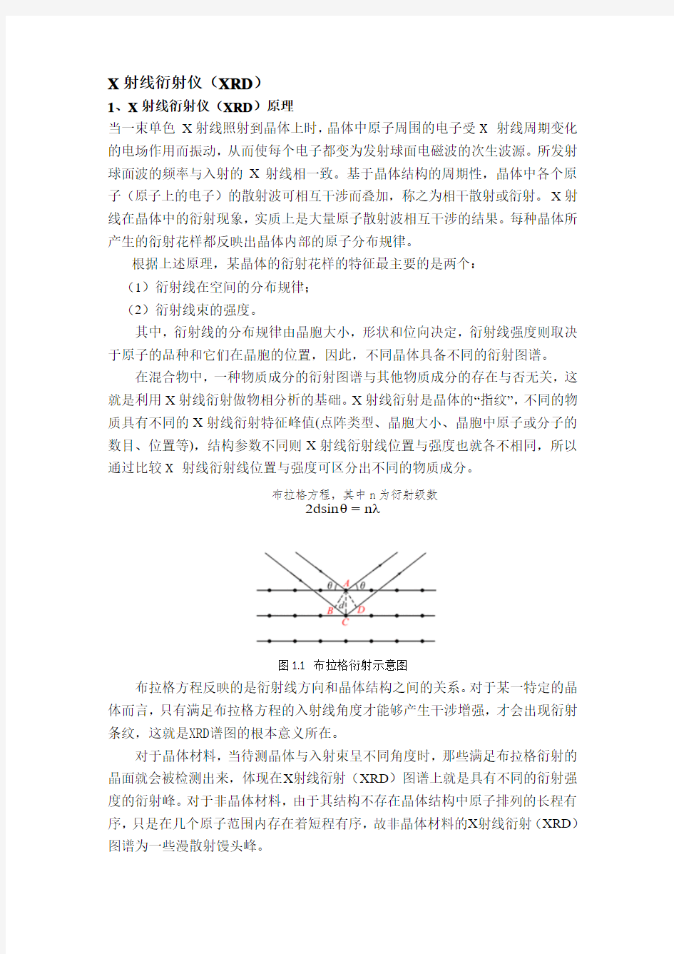
布拉格方程,其中n 为衍射级数
图1.1 布拉格衍射示意图
布拉格方程反映的是衍射线方向和晶体结构之间的关系。对于某一特定的晶体而言,只有满足布拉格方程的入射线角度才能够产生干涉增强,才会出现衍射条纹,这就是XRD 谱图的根本意义所在。
对于晶体材料,当待测晶体与入射束呈不同角度时,那些满足布拉格衍射的晶面就会被检测出来,体现在X 射线衍射(XRD )图谱上就是具有不同的衍射强度的衍射峰。对于非晶体材料,由于其结构不存在晶体结构中原子排列的长程有序,只是在几个原子范围内存在着短程有序,故非晶体材料的X 射线衍射(XRD )图谱为一些漫散射馒头峰。
n λ
=2dsin θ
应用已知波长的X射线来测量θ角,从而计算出晶面间距d,这是用于X射线结构分析;另一个是应用已知d的晶体来测量θ角,从而计算出特征X射线的波长,进而可在已有资料中查出试样中所含的元素。
2、X射线衍射仪(XRD)的简单应用
(1)X射线衍射仪(XRD)研究的是材料的体相结构,X射线衍射仪(XRD)采用单色X射线为衍射源,因此X射线衍射仪(XRD)给出的是材料的体相结构信息。
(2)XRD即是定性分析手段亦是定量分析手段,XRD多以定性物相分析为主,但也可以进行定量分析。通过待测样品的X射线衍射谱图与标准物质的X 射线衍射谱图进行对比,可以定性分析样品的物相组成,通过对样品衍射强度数据的分析计算,可以完成样品物相组成的定量分析。
(3)XRD进行定性分析时可以得到下列信息
A.根据XRD谱图信息,可以确定样品是无定型还是晶体:无定型样品为大包峰,没有精细谱峰结构;晶体则有丰富的谱线特征。把样品中最强峰的强度和标准物质的进行对比,可以定性知道样品的结晶度。
B. 通过与标准谱图进行对比,可以知道所测样品由哪些物相组成(XRD最主要的用途之一)。基本原理:晶态物质组成元素或基团如果不相同或其结构有差异,它们的衍射谱图在衍射峰数目、角度位置、相对强度以及衍射峰形上会显现出差异(基于布拉格方程,后面会详细解析)。
C. 通过实测样品和标准谱图2θ值的差别,可以定性分析晶胞是否膨胀或者收缩的问题,因为XRD的峰位置可以确定晶胞的大小和形状。
(4)X射线衍射仪(XRD)定量分析可应用下列内容
A.样品的平均晶粒尺寸,基本原理:当X射线入射到小晶体时,其衍射线条将变得弥散而宽化,晶体的晶粒越小,X射线衍射谱带的宽化程度就越大。因此晶粒尺寸与XRD谱图半峰宽之间存在一定的关系,即谢乐公式(Scherrerequation)
B.样品的相对结晶度:一般将最强衍射峰积分所得的面积(As)当作计算结晶度的指标,与标准物质积分所得面积(Ag)进行比较,结晶度=As/Ag*100%。
C.物相含量的定量分析:主要有K值法也叫RIR方法和Rietveld全谱精修定量等。其中,RIR法的基本原理为1:1混合的某物质与刚玉(AL2O3),其最强衍射峰的积分强度会有一个比值,该比值为RIR值。通过将该物质的积分强度/RIR 值总是可以换算成Al2O3的积分强度。对于一个混合物而言,物质中所有组分都按这种方法进行换算,最后可以通过归一法得到某一特定组分的百分含量。
D. XRD还可以用于点阵常数的精密计算,残余应力计算等。
3、X射线衍射仪(XRD)基本构造
(1)X射线发生器(产生X射线的装置);
(2)测角仪(测量角度2θ的装置);
(3)X射线探测器(测量X射线强度的计数装置);
(4)X射线系统控制装置(数据采集系统和各种电气系统、保护系统等)。
1、Epitaxial growth of a methoxy-functionalized quaterphenylene on alkali halide surfaces
(Thin Solid FilmsVolume 597, 31 December 2015, Pages 104–111)(1)For characterization of epitaxy and the domain structure, a combination of low energy electron diffraction (LEED), X-ray diffraction (XRD), various optical microscopy techniques, and atomic force microscopy (AFM) is used.
(2) Contact planes are determined by X-ray diffraction using a PANalytical
X'PertPro MPD diffractometer in Bragg–Brentano geometry (Cu Kα radiation), film texture is investigated by X-ray diffraction pole figures.
(3)To resolve the thin film structure perpendicular to the substrate surface, XRD patterns have been collected. Due to the insensitivity of the XRD apparatus, the organic films have to be a factor of ten to fifty thicker than the previously investigated ones. In Fig. 4(a), diffractograms are shown for thick (between 200 and 300 nm) MOP4 films deposited at room temperature on KCl, NaCl, and on glass. In all cases, a series of peaks is observed, which indicates highly ordered material. The peak positions are close to the calculated positions of the (00.2n) peaks from the bulk (001) face (dashed vertical lines) [56]. For MOP4 on glass, e.g., peaks up to 2n = 32 are detected. The peaks are slightly shifted to smaller angle values, whereas for MOP4 powder dispersed on glass, the bulk crystal positions of the (00.2n) peaks are exactly reproduced. The upright molecules in this substrate-induced phase have a 0.36(5) ? larger d-spacing, see the shaded area in Fig. 4(b), and, thus probably are by a few degrees more upright with respect to the (001) plane as in a single layer of the bulk phase (tilt angle approximately 66°). Similar surface-induced phases have been observed for, e.g., the thin-film growth of para-hexaphenylene [61]
and [62] and pentacene [63] on SiO2.For NaCl and KCl, additional peaks are observed besides the substrate peaks (marked by asterisks, higher harmonics as well as diffraction of Cu Kβ radiation), stemming from lying MOP4 molecules on the surface (”L”), i.e., most probably from nanofibers. The broad backgrounds for KCl and NaCl originate from diffracted bremsstrahlung.
2、Nanocrystalline titanium films deposited via thermal-emission-enhanced magnetron sputtering
(Thin Solid FilmsVolume 597, 31 December 2015, Pages 117–124
(1)Nanocrystalline titanium films were deposited at ultra-high current density by a direct-current closed-field unbalanced magnetron sputtering technique. The structures and properties of the films were characterized using X-ray diffraction (XRD), scanning electron microscopy (SEM), transmission electron microscopy (TEM), atomic force microscopy (AFM) and nanoindentation microscratch.
(2)The crystal structures of the films were characterized by an XRD-7000S
X-ray diffractometer (XRD, SHIMADZU-LIMITED Corp.) from 30°to 80° at an increment of 0.02°. The grain sizes of the films were calculated from the (101) diffraction peak according to Scherrer's equation[24] and [25]:t=0.9 /(Bcosθ) where λ is the X-ray wavelength (0.15406 nm for Cu), θ is the Bragg angle of the diffraction peak, and B is the full-width-half-maximum (FWHM) of the peak.
(3)Fig. 3 shows the XRD patterns of samples A to E. The pattern of sample A only had a low-density diffraction peak at 2θ = 35°, indicating the film microstructure was nanocrystalline with very small grain sizes. Samples B to E each exhibited a hexagonal close packed (hcp) structure, based on the JCPDS card #
44-1294. It showed diffraction peaks (100), (002), (101), (102), (110), (103) and (112). The average grain sizes of samples B to E were 6, 14, 15 and 16 nm, respectively, indicating the grain sizes increased with the current density. The XRD patterns also indicated that the preferred orientations of samples A to E were (100), (100)/(002), (002), (002)/(101) and (101), respectively. The preferred orientation gradually changed from (100) to (101) with Id increased.
Fig. 3. XRD pattern of samples A to E.
3、Two-Dimensional Vanadium Carbide (MXene) as Positive Electrode for Sodium-Ion Capacitors