ip5306中文资料_数据手册_参数
- 格式:pdf
- 大小:2.58 MB
- 文档页数:12

IRF5305HEXFET ® Power MOSFETPD - 91385BFifth Generation HEXFETs from International Rectifier utilize advanced processing techniques to achieve extremely low on-resistance per silicon area. This benefit,combined with the fast switching speed and ruggedized device design that HEXFET Power MOSFETs are well known for, provides the designer with an extremely efficient and reliable device for use in a wide variety of applications.The TO-220 package is universally preferred for all commercial-industrial applications at power dissipation levels to approximately 50 watts. The low thermal resistance and low package cost of the TO-220 contribute to its wide acceptance throughout the industry.ParameterMax.UnitsI D @ T C = 25°C Continuous Drain Current, VGS @ -10V -31ID @ T C = 100°C Continuous Drain Current, V GS @ -10V -22A I DMPulsed Drain Current -110P D @T C = 25°C Power Dissipation 110W Linear Derating Factor 0.71W/°C V GS Gate-to-Source Voltage± 20V E AS Single Pulse Avalanche Energy 280mJ I AR Avalanche Current-16A E AR Repetitive Avalanche Energy 11mJ dv/dt Peak Diode Recovery dv/dt -5.0V/ns T J Operating Junction and-55 to + 175T STGStorage Temperature RangeSoldering Temperature, for 10 seconds 300 (1.6mm from case )°CMounting torque, 6-32 or M3 srew10 lbf•in (1.1N•m)Absolute Maximum RatingsParameterTyp.Max.UnitsR θJC Junction-to-Case––– 1.4R θCS Case-to-Sink, Flat, Greased Surface 0.50–––°C/WR θJAJunction-to-Ambient–––62Thermal Resistancel Advanced Process Technology l Dynamic dv/dt Ratingl 175°C Operating Temperature l Fast Switching l P-ChannellFully Avalanche RatedDescription3/3/00IRF5305IRF5305IRF5305IRF5305IRF5305IRF5305IRF5305。


NEC’s NX5306 series is a 1310 nm Multiple Quantum Well (MQW) structured Fabry-Perot (FP) laser diode with InGaAs monitor PIN-PD. This device is ideal for Synchronous Digital Hierarchy (SDH) systems, long haul STM-1 (L-1.1), short haul STM-4 (S-4.1), and ITU-T recommendations.California Eastern LaboratoriesNX5306 SERIESPACKAGE DIMENSIONS (Units in mm)NX5306 SERIES ORDERING INFORMATIONRemarks 1.The color of ball lens cap might be observed differently from ourcan package products.2.The hermetic test will be performed as AQL 1.0%.NX5306 SERIESABSOLUTE MAXIMUM RATINGSPARAMETER SYMBOL RATINGS UNIT Optical Output Power P o20mW Forward Current of LD I F150mA Reverse Voltage of LD V R 2.0V Forward Current of PD I F10mA Reverse Voltage of PD V R20V Operating Case Temperature T C−40 to +85°C Storage Temperature T stg−40 to +85°C Assembly Temperature T asb150 (15 Hr)°C Lead Soldering Temperature T sld350 (3 sec.)°C Relative Humidity (noncondensing)RH85%NX5306 SERIESELECTRO-OPTICAL CHARACTERISTICS (T C = -25°C, unless otherwise speci Þ ed)PARAMETERSYMBOL CONDITIONSMIN.TYP .MAX.UNIT Operating Voltage V op P o = 5.0 mW, T C = −40 to +85°C1.1 1.5V Threshold CurrentI th1015mAT C = 85°C2530Threshold Output Power P th T C = −40 to +85°C, I F = I th100200μW Differential Ef Þ ciency ηd 0.320.4W/A Temperature Dependence of Differential Ef Þ ciency Δηd Δηd = 10 log−3.0−1.2dB Center WavelengthλC P o = 5.0 mW, RMS (−20 dB)T C = −40 to +85°C 1 2631 360nm Temperature Dependence of Center Wavelength Δλ/ΔT T C = −40 to +85°C0.40.5nm/°C Spectral Width σP o = 5.0 mW, RMS (−20 dB)T C = −40 to +85°C 1.0 2.5nm Rise Time t r 10-90%0.150.3ns Fall Time t f 90-10%0.150.3ns Monitor Current I m V R = 5 V, P o = 5.0 mW 150300600μA Monitor Dark CurrentI DV R = 5 V0.110nAV R = 5 V, T C = −40 to +85°C500Monitor PD Terminal Capacitance C t V R = 5 V, f = 1 MHz620pF Tracking Error *1γI m = const. (@ P o = 5.0 mW, T C = 25°C)T C = −40 to +85°C−1.01.0dB ηd (@85ºC)ηd (@25ºC)*1 Tracking Error: γI mC = -40 to +85ºCP o(mW)P (mA)γ = 10 log[dB]P o 5.0NX5306 SERIESTYPICAL CHARACTERISTICS (T C = −40 to +85°C, unless otherwise speci Þ ed)Remark The graphs indicate nominal characteristics.Forward Current I F (mA)O p t i c a l O u t p u t P o w e r P o (m W )OPTICAL OUTPUT POWER vs. FORWARD CURRENTOPERATING CURRENT AND THRESHOLD CURRENT vs. CASE TEMPERATURECase Temperature T C (ºC)O p e r a t i n g C u r r e n t I o p (m A ),T h r e s h o l d C u r r e n t I t h (m A )123510203050100-40-2020406080100-60I op I thTEMPERATURE DEPENDENCE OF CENTER WAVELENGTHCase Temperature T C (ºC)C e n t e r W a v e l e n g t h λC (n m )1 3401 2801 3001 320-20-40-6020604080100NX5306 SERIESA Business Partner of NEC Compound Semiconductor Devices, Ltd.08/03/2004Life Support ApplicationsThese NEC products are not intended for use in life support devices, appliances, or systems where the malfunction of these products can reasonably be expected to result in personal injury. The customers of CEL using or selling these products for use in such applications do so at their own risk and agree to fully indemnify CEL for all damages resulting from such improper use or sale.TYPICAL CHARACTERISTICS (T C = 25°C, unless otherwise speci Þ ed)SPECTRUMR e l a t i v e I n t e n s i t yWavelength λ (nm)1 3101 300 1 320TOLERANCE OF FIBER COUPLING DISTANCE (Z)Z-Axis Tolerance Z (mm)O t i c a l O u t p u t P o w e r f r o m F i b e r P f (m W )FORWARD CURRENT vs.FORWARD VOLTAGEF o r w a r d C u r r e n t I F (m A )Forward Voltage V F (V)12403020105003009006001050O p t i c a l O u t p u t P o w e r P o (m W )OPTICAL OUTPUT POWER vs. MONITOR CURRENTMonitor Current I m ( A)µRemark The graphs indicate nominal characteristics.。


IRFR/U5305HEXFET ® Power MOSFETFifth Generation HEXFETs from International Rectifier utilize advanced processing techniques to achieve extremely low on-resistance per silicon area. This benefit, combined with the fast switching speed and ruggedized device design that HEXFET ® Power MOSFETs are well known for, provides the designer with an extremely efficient and reliable device for use in a wide variety of applications.The D-Pak is designed for surface mounting using vapor phase, infrared, or wave soldering techniques. The straight lead version (IRFU series) is for through-hole mounting applications. Power dissipation levels up to 1.5 watts are possible in typical surface mount applications.ParameterMax.UnitsI D @ T C = 25°C Continuous Drain Current, V GS@ -10V -31I D@ TC= 100°C Continuous Drain Current, V GS @ -10V -22A I DMPulsed Drain Current -110P D @T C = 25°C Power Dissipation 110W Linear Derating Factor 0.71W/°C V GS Gate-to-Source Voltage± 20V E AS Single Pulse Avalanche Energy 280mJ I AR Avalanche Current-16A E AR Repetitive Avalanche Energy 11mJ dv/dt Peak Diode Recovery dv/dt -5.0V/ns T J Operating Junction and -55 to + 175T STGStorage Temperature RangeSoldering Temperature, for 10 seconds 300 (1.6mm from case )°CMounting torque, 6-32 or M3 srew10 lbf•in (1.1N•m)Absolute Maximum RatingsParameterTyp.Max.UnitsR θJC Junction-to-Case––– 1.4R θJA Junction-to-Ambient (PCB mount)*–––50°C/WR θJAJunction-to-Ambient**–––110Thermal ResistancelUltra Low On-Resistance l Surface Mount (IRFR5305)l Straight Lead (IRFU5305)l Advanced Process Technology l Fast Switchingl Fully Avalanche RatedDescription10/23/00D-Pak I-Pak IRFR5305 IRFU5305PD - 91402AIRFR/U5305IRFR/U5305IRFR/U5305IRFR/U5305IRFR/U5305IRFR/U5305IRFR/U5305IRFR/U5305IRFR/U5305。

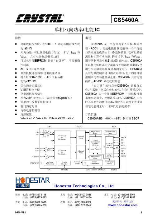
摘要T PS 5430是TI ( 美国德州仪器公司) 推出的一款性能优越的DC /DC开关电源转换芯片。
TPS5430 特性
TPS 5430具有良好的特性, 其各项性能及主要参数如下:
高电流输出: 3 A ( 峰值 4 A ) ; 宽电压输入范围: 515 ~36 V;
高转换效率: 最佳状况可达95 % ; 宽电压输出范围: 最低可以调整降到11221 V;
内部补偿最小化了外部器件数量; 固定500 kHz转换速率;
有过流保护及热关断功能; 具有开关使能脚, 关状态仅有17 u A 静止电流;
内部软启动
与其他同类型直流开关电源转换芯片相比, TPS 5430 的高转换效率特别值得关注。
图
1 为在1
2 V 输入电压、5 V 输出电压时TPS 5430 转换效率与输出电流的关系曲线图。
1: BOOT脚, FET门驱动; 2: 空; 3: 空; 4: VSENSE脚, 误差放大器转换节点, 基准电压值; 5: 使能脚; 6: 地;
7: 电压输入脚; 8: PH脚, 相位端, 与外部LC滤波器连接; 9: Po wer P AD 脚, 与过孔焊盘连接, 用于散热
最初, 我们曾采用MAX1626等芯片电源为T J - 2型体积式应变仪数据采集系统供电,
但在测试中我们发现系统工作不稳定, 仪器会出现自动重启现象。
究其原因, 发现是MAX1626等芯片电源带负载能力不足够大造成的。
因此, 经过多方考察, 我们最终选用带负载能力强、效率高、外围器件少的TPS 5430 芯片作电源, 为数据采集系统的 A /D 转换模块和数据处理模块供电,。

FT5x06True Multi-TouchCapacitive TouchPanel ControllerINTRODUCTIONThe FT5x06 Series ICs are single-chip capacitive touch panel controller ICs with a built-in 8 bit Micro-controller unit (MCU).They adopt the mutual capacitance approach, which supports true multi-touch capability. In conjunction with a mutual capacitive touch panel, the FT5x06 have user-friendly input functions, which can be applied on many portable devices, such as cellular phones, MIDs, netbook and notebook personal computers.The FT5x06 series ICs include FT5206/FT5306/FT5406, the difference of their specifications will be listed individually in this datasheet.FEATURESz Mutual Capacitive Sensing Techniquesz True Multi-touch with up to 10 Points of Absolution X and Y Coordinates z Immune to RF Interferencesz Auto-calibration: Insensitive to Capacitance and Environ-mental Variations z Supports up to 28 Transmit Lines and 16 Receive Lines z Supports up to 8.9” Touch Screenz Full Programmable Scan Sequences with Individual Ad-justable Receive Lines and Transmit Lines to Support Various Applications z High Report Rate: More than 100Hzz Touch Resolution of 100 Dots per Inch (dpi) or above -- depending on the Panel Size z Optional Interfaces :I2C/SPI z 2.8V to 3.6V Operating Voltage z Supports 1.8V/AVDD IOVCCz Capable of Driving Single Channel (transmit/receive) Re-sistance: Up to15K Ω z Capable of Supporting Single Channel (transmit/receive) Capacitance: 60 pF z Optimal Sensing Mutual Capacitor: 1pF~4pF z 12-Bit ADC Accuracyz Built-in MCU with 28KB Program Memory, 6KB Data Memory and 256B Internal Data Space z 11 Internal Interrupt Sources and 2 External Interrupt Sources z 3 Operating Modes¾ Active ¾ Monitor ¾ Hibernatez Operating Temperature Range: -40°C to +85°CFT5x06 ArrayDATASHEETINTRODUCTION (I)FEATURES (I)1 OVERVIEW (1)1.1 T YPICAL A PPLICATIONS (1)2 FUNCTIONAL DESCRIPTION (1)2.1 A RCHITECTURAL O VERVIEW (1)2.2 MCU (2)2.3 O PERATION M ODES (2)2.4 H OST I NTERFACE (3)2.5 S ERIAL I NTERFACE (3)2.5.1 I2C (3)2.5.2 SPI (4)3 ELECTRICAL SPECIFICATIONS (8)3.1 A BSOLUTE M AXIMUM R ATINGS (8)3.2 DC C HARACTERISTICS (9)3.3 AC C HARACTERISTICS (9)3.4 I/O P ORTS C IRCUITS (10)3.5 POWER ON/R ESET/W AKE S EQUENCE (11)4 PIN CONFIGURATIONS (12)5 PACKAGE INFORMATION (15)5.1 P ACKAGE I NFORMATION OF QFN-5X5-40L P ACKAGE (15)5.2 P ACKAGE I NFORMATION OF QFN-6X6-48L P ACKAGE (16)5.3 P ACKAGE I NFORMATION OF QFN-8X8-68L P ACKAGE (17)5.4 O RDER I NFORMATION (18)1OVERVIEW1.1Typical ApplicationsFT5x06 accommodate a wide range of applications with a set of buttons up to a 2D touch sensing device, their typical applications are listed below.z Mobile phones, smart phonesz MIDsz Netbookz Navigation systems, GPSz Game consolesz Car applicationsz POS (Point of Sales) devicesz Portable MP3 and MP4 media playersz Digital camerasFT5x06 Series ICs support 2.8”~8.9” Touch Panel, users may find out their target IC from the specs. listed in the following table,Panel PackageModel NameTouch Panel SizeTX RX Type Pin SizeFT5206GE1 15 10 QFN5*5 40 0.75-P0.4 2.8"~3.8"FT5306DE4 20 12 QFN6*6 48 0.75-P0.4 4.3"~7"FT5406EE8 28 16 QFN8*8 68 0.75-P0.4 7"~8.9"2FUNCTIONAL DESCRIPTION2.1Architectural OverviewFigure2-1 shows the overall architecture for the FT5x06.Figure 2-1 FT5x06 System Architecture DiagramThe FT5x06 is comprised of five main functional parts listed below,z Touch Panel Interface CircuitsThe main function for the AFE and AFE controller is to interface with the touch panel. It scans the panel by sending AC signals to the panel and processes the received signals from the panel. So, it supports both Transmit (TX) and Receive (RX) functions. Key pa-rameters to configure this circuit can be sent via serial interfaces, which will be explained in detail in a later section.z8051-based MCUThis MCU is 8051 compatible with some enhancements. For instant, larger program and data memories are supported. In addition, a Multiplication-Division unit (MDU) is implemented to speed up the touch detection algorithms. Furthermore, a Flash ROM is implemented to store programs and some key parameters.Complex signal processing algorithms are implemented with firmware running on this MCU to process further the received signals in order to detect the touches reliably. Communication protocol software is also implemented on this MCU to exchange data and control information with the host processor.z External Interface¾I2C/SPI: an interface for data exchange with host¾INT: an interrupt signal to inform the host processor that touch data is ready for read¾WAKE: an interrupt signal for the host to change F5x06 from Hibernate to Active mode¾/RST: an external low signal reset the chip.z A watch dog timer is implemented to ensure the robustness of the chip.z A voltage regulator to generate 1.8V for digital circuits from the input VDD3 supply2.2MCUThis section describes some critical features and operations supported by the 8051 compatible MCU.Figure 2-2 shows the overall structure of the MCU block. In addition to the 8051 compatible MCU core, we have added the following circuits,z MDU: A 16x8 Multiplier and A 32/32 Dividerz Program Memory: 28KB Flashz Data Memory: 6KB SRAMz Real Time Clock (RTC): A 32KHz RC Oscillatorz Timer: A number of timers are available to generate different clocksz Master Clock: 24/ 48MHz from a 48MHz RC Oscillatorz Clock Manager: To control various clocks under different operation conditions of the systemFigure 2-2 MCU Block Diagram2.3Operation ModesFT5x06 operates in the following three modes:z Active ModeWhen in this mode, FT5x06 actively scans the panel. The default scan rate is 60 frames per second. The host processor can configure FT5x06 to speed up or to slow down.z Monitor ModeWhen in this mode, FT5x06 scans the panel at a reduced speed. The default scan rate is 25 frames per second and the host processor can increase or decrease this rate. When in this mode, most algorithms are stopped. A simpler algorithm is being executed to de-termine if there is a touch or not. When a touch is detected, FT5x06 shall enter the Active mode immediately to acquire the touch information quickly. During this mode, the serial port is closed and no data shall be transferred with the host processor. z Hibernate ModeIn this mode, the chip is set in a power down mode. It shall only respond to the “WAKE” or “RESET” signal from the host processor. The chip therefore consumes very little current, which help prolong the standby time for the portable devices.2.4 Host InterfaceFigure 2-3 shows the interface between a host processor and FT5x06. This interface consists of the following three sets of signals: z Serial Interfacez Interrupt from FT5x06 to the Host z Wake-up Signal from the Host to FT5x06Figure 2-3 Host Interface DiagramThe serial interfaces of FT5x06 is I2C or SPI. The details of this interface are described in detail in Section 2.5. The interrupt signal (/INT) is used for FT5x06 to inform the host that data are ready for the host to receive. The /WAKE signal is used for the host to wake up FT5x06 from the Hibernate mode. After exiting the Hibernate mode, FT5x06 shall enter the Active mode.2.5 Serial InterfaceFT5x06 supports the I2C or SPI interfaces, which can be used by a host processor or other devices.2.5.1 I2CThe I2C is always configured in the Slave mode. The data transfer format is shown in Figure 2-4.Figure 2-4 I2C Serial Data Transfer FormatFigure 2-5 I2C master write, slave readFigure 2-6 I2C master read, slave writeTable 2-1 lists the meanings of the mnemonics used in the above figures.Table 2-1 Mnemonics DescriptionMnemonicsDescriptionS I2C Start or I2C RestartA[6:0]Slave address A[6:4]: 3’b011A[3:0]: data bits are identical to those of I2CCON[7:4] register.W 1’b0: Write R 1’b1: Read A(N) ACK(NACK) PSTOP: the indication of the end of a packet (if this bit is missing, S will indicate the endof the current packet and the beginning of the next packet)I2C Interface Timing Characteristics is shown in Table 2-2.Table 2-2 I2C Timing CharacteristicsParameterUnit Min Max SCL frequencyKHz 0 400 Bus free time between a STOP and START condition us 4.7 \ Hold time (repeated) START condition us 4.0 \ Data setup timens 250 \ Setup time for a repeated START condition us 4.7 \ Setup Time for STOP conditionus4.0\2.5.2 SPISPI is a 4 wire serial interface. The following is a list of the 4 wires: z SCK: serial data clockz MOSI: data line from master to slave z MISO: data line from slave to master z SLVESEL: active low select signalSPI transfers data at 8bit packets. The phase relationship between the data and the clock can be defined by the two registers: phase and polck. Some data transfer examples can be found in Figure 2-7 to Figure 2-10.Figure 2-7 SPI Data Transfer Format (Phase=0, POLCK=0)Figure 2-8 SPI Data Transfer Format (PHASE=0, POLCK=1)bit7bit6bit5bit4bit3bit2bit1bit0MSBMISO/MOSISCKSLVSELPHASE=1 POLE=0Figure 2-9 SPI Data Transfer Format (Phase=1, POLCK=0)Figure 2-10 SPI Data Transfer Format (Phase=1, POLCK=1)SPI can be configured into either Master or Slave mode via the MAS bit of the SPI0CON register. When in the Master mode, the SPI needs to supply the data clock, whose frequency relationship with the Master clock can be set by CLKDVD bits of the SPI0CON register. When it is configured in the Slave mode, the clock, SCK, is supplied by the external Master. The maximum data clockfrequency must not be higher than8mclkF.SPI Interface Timing Characteristics is shown in the following Figure2-11,Figure2-12, Figure2-13, Figure2-14 and Table 2-3.MOSI SCK(POLCK=0)SLVSELMISO Tmckh TmcklTmsf cSCK(POLCK=1)PHASE=0Tmsr cTmoTmhTsdFigure 2-11 SPI master Timing PHASE =0MOSI SCK(POLCK=0)SLVSELMISO TmckhTmckl TmsfcSCK(POLCK=1)PHASE=1TmoTmhTmsr cFigure 2-12 SPI master Timing PHASE =1Figure 2-13 SPI slave Timing PHASE = 0MOSI SCK(POLCK=0)SLVSELMISOTsckhTsckl T sThToTsfcSCK(POLCK=1)PHASE=1Tsr cFigure 2-14 SPI slave Timing PHASE = 1Table 2-3 SPI Timing ParametersParameter Description MinMax UnitsMaster Mode timing (see figure 2-11,2-12)Tmckh sck high time 4×Tsysclk -- ns Tmckl sck low time4×Tsysclk-- ns Tmo sck shift edge to mosi data change 0 --nsTmh mosi data valid to sck shift edge 3×Tsysclk -- ns Tsd slvsel falling edge to mosi data valid 4×Tsysclk -- ns Tmsfcslvsel falling edge to first sck edge(Tmckh+Tmckl)/2--nsTmsrc last sck edge to slvsel rising edge (Tmckh+Tmckl)/2-- nsSlave mode timing(See figure 2-13,2-14)Tsckh sck high Time 4×Tsysclk -- ns Tsckl sck low Time 4×Tsysclk -- ns Tsd slvsel falling edge to Miso valid data time 0 4xTsysclk nsTs Mosi Data valid to sck sample edge 0 -- nsTh sck sample edge to Mosi data change 4×Tsysclk -- ns To sck shift edge to Miso data change 0 4xTsysclk nsTsfc slvsel falling edge to first sck edge 4×Tsysclk -- ns Tsrc last sck edge to slvsel rising edge 4×Tsysclk -- ns *Tsysclk is equal to one period of the device system clock3ELECTRICAL SPECIFICATIONS3.1Absolute Maximum RatingsTable 3-1 Absolute Maximum RatingsItem Symbol Unit Value Note Power Supply Voltage 1 VDDA - VSSA V -0.3 ~ +3.6 1, 2Power Supply Voltage 2 VDD3 – VSS V -0.3 ~ +3.6 1, 3I/O Power Supply Voltage Vt V -0.3 ~ IOVCC + 0.3 1,4Operating Temperature Topr ℃-40 ~ +85 1Storage Temperature Tstg ℃-55 ~ +125 1Notes1.If used beyond the absolute maximum ratings, FT5x06 may be permanently damaged. It is strongly recommended that the devicebe used within the electrical characteristics in normal operations. If exposed to the condition not within the electrical characteristics,it may affect the reliability of the device.2.Make sure VDDA(high)≥VSSA (low)3.Make sure VDD (high)≥VSS (low)4.IOVCC is set to VDD3 or VDDD by software configuration.3.2DC CharacteristicsTable 3-2 DC Characteristics (VDDA=VDD3=2.8~3.6V, Ta=-40~85℃)Item Symbol Unit Test Condition Min. Typ. Max. Note Input high-level voltage VIH V 0.7 x IOVCC -- IOVCCInput low -level voltage VIL V -0.3 -- 0.3 x IOVCCOutput high -level voltage VOH V IOH=-0.1mA 0.7 x IOVCC -- --Output low -level voltage VOL V IOH=0.1mA -- -- 0.3 x IOVCCI/O leakage current ILI μA Vin=0~VDDA -1 --1Current consumption (Normal operation mode)Iopr mAVDDA=VDD3 = 2.8VTa=25℃ MCLK=24MHz-- 6--Current consumption (Monitor mode)Imon mAVDDA=VDD3 = 2.8VTa=25℃ MCLK=24MHz-- 4--Current consumption (Sleep mode)Islp mAVDDA=VDD3 = 2.8VTa=25℃ MCLK=24MHz-- 0.03--Step-up output voltage VDD5 V VDDA=VDD3= 2.8V 5 5.255.6Power Supply voltage VDDAVDD3 V 2.7 2.8~3.63.73.3AC CharacteristicsTable 3-3 AC Characteristics of OscillatorsItem Symbol Unit Test Condition Min. Typ. Max. NoteOSC clock 1 fosc1 MHz VDD3 = 2.8VTa=25℃43 48 52OSC clock 2 fosc2 KHz VDD3 = 2.8VTa=25℃29 32 36Table 3-4 AC Characteristics of TX & RXItem Symbol Unit Test Condition Min Typ Max Note TX acceptable clock ftx KHz 100 150 270TX output rise time Ttxr nS -- 20 --TX output fall time Ttxf nS -- 20 --RX input voltage Trxi V 1.2 -- 1.63.4 I/OPortsCircuitsFigure 3-1 Digital Input & Output Port CircuitsFigure 3-2 Digital In/Out Port CircuitFigure 3-3 Reset Input Port Circuits Figure 3-4 Wake Input Port CircuitsFigure 3-5 INT output Port Circuits Figure 3-6 SCL/SDA Port Circuits3.5POWER ON/Reset/Wake SequenceThe GPIO such as Wake, INT and I2C should be pulled down to be low before powering on. The signal of waking up should be set to be high after powering on. INT signal will be sent to the host after initializing all parameters and then start to report points to the host.Powe rFigure 3-7 Power on timePow er I NT I 2C/SPIW akeup Figure 3-8 Power on SequenceReset time must be enough to guarantee reliable reset, The time of starting to report point after resetting approach to the time ofstarting to report point after powering on.Pow er I NT I 2C/SPIRESETFigure 3-8 Reset SequenceWake time must be enough to wake up the system, The time of starting to report point after waking approach to the time of starting to report point after powering onPow er I NT I 2C/SPIW ak eupFigure 3-8 Wake SequenceTable 3-5 Power on/Reset/Wake Sequence ParametersParameterDescriptionMin Max Units Tris Rise time from 0.1VDD to 0.9VDD-- 10 ms Tpon Time of starting to report point after powering on 300 -- ms Trsi Time of starting to report point after resetting 300 -- ms Trst Reset time5 -- ms Twai Time of starting to report point after waking 300 -- ms TwakWake up time5--ms4 PIN CONFIGURATIONSPin List of FT5x06Table 4-1 Pin Definition of FT5x06Pin No.NameFT5206GE1FT5306DE4FT5406EE8Type DescriptionVSSA 40 1 1 PWRAnalog groundNC 1 2 2 Not connected NC 48 3 Not connected TX28 4 O Transmit output pin TX27 5 O Transmit output pin TX26 6 O Transmit output pin TX25 7 O Transmit output pin TX24 8 O Transmit output pin TX23 9 O Transmit output pin TX22 10 O Transmit output pin TX21 11 O Transmit output pin TX20 3 12 O Transmit output pin TX19 4 13 O Transmit output pin TX18 5 14 O Transmit output pin TX17 6 15 O Transmit output pin TX16 7 16 O Transmit output pin TX15 2 8 17 O Transmit output pin TX143918OTransmit output pinTX13 4 10 19 O Transmit output pin TX12 5 11 20 O Transmit output pin TX11 6 12 21 O Transmit output pin TX10 7 13 22 O Transmit output pin TX9 8 14 23 O Transmit output pin TX8 9 15 24 O Transmit output pin TX7 10 16 25 O Transmit output pin TX6 11 17 26 O Transmit output pin TX5 12 18 27 O Transmit output pin TX4 13 19 28 O Transmit output pin TX3 14 20 29 O Transmit output pin TX2 15 21 30 O Transmit output pin TX1 16 22 31 O Transmit output pinVDD5 17 23 32PWR internal generated 5V power supply, A 1μF ceramic capacitor to ground is required.VDD3 18 24 33 PWR Analog power supplyVSS 19 25 34PWR AnaloggroundVDDD 20 26 35PWR Digital power supply (1.8V), generated internal. A 1μF ceramic capacitor to ground is required.TEST_EN 21 27 36 I Test mode enabled at high and float in normal mode GPIO0 37 I/O General Purpose Input/Output portGPIO1 38 I/O General Purpose Input/Output portGPIO2 39 I/O General Purpose Input/Output portGPIO3 40 I/O General Purpose Input/Output portSSEL/SCL 22 28 41 I/O SPI Slave mode, chip select, active low / I2C clock input SCK 23 29 42 I SPI Slave mode, clock inputMOSI/SDA 24 30 43 I/O SPI Slave mode, data input / I2C data input and output MISO 25 31 44 O SPI Slave mode, data output/RST 26 32 45 I External Reset, Low is activeWAKE 27 33 46 I External interrupt from the hostINT 28 34 47 O External interrupt to the hostNC 48 Notconnected NC 49 Notconnected NC 50 Notconnected NC 51 NotconnectedVDDA 30 35 52 PWR Analog power supplyRX1 29 36 53 I Receiver input pinsRX2 31 37 54 I Receiver input pinsRX3 32 38 55 I Receiver input pinsRX4 33 39 56 I Receiver input pinsRX5 34 40 57 I Receiver input pinsRX6 35 41 58 I Receiver input pinsRX7 36 42 59 I Receiver input pinsRX8 37 43 60 I Receiver input pinsRX9 38 44 61 I Receiver input pinsRX10 39 45 62 I Receiver input pinsRX11 46 63 I Receiver input pins RX12 47 64 I Receiver input pins RX13 65 I Receiver input pins RX14 66 I Receiver input pins RX15 67 I Receiver input pins RX1668IReceiver input pinsFT5206GE1 Package Diagram FT5306DE4 Package DiagramFT5406EE8 Package DiagramVSSA NC NC TX28TX27TX26TX25TX24345TX18TX15NCNC NCNCINT WAKESSEL/SCL45/RST MOSI/SDA 515049484746GPIO1VDDDT X 14T X 1T X 12T X 11T X 10T X 9T X 5T X 4T X 32425262728T X8TX7T X 6T X 2T X 1V D D 5V D D 3V S SV D D A R X 1R X 2X 3R X 4X 5X 9X 10X 1158R X 6X 7X 852535456R X 126465R X 13X 14R X 1567X 165PACKAGE INFORMATION5.1Package Information of QFN-5x5-40L PackageMillimeter ItemSymbolMin Typ MaxTotal Thickness A 0.7 0.75 0.8Stand OffA1 0 0.035 0.05 Mold Thickness A2 ----0.55 0.57L/F Thickness A3 0.203 REF Lead Width b 0.150.20 0.25 D 5 BSC Body Size E 5 BSC Lead Pitch e 0.4 BSC J 3.5 3.6 3.7 EP SizeK 3.5 3.6 3.7 Lead LengthL 0.350.4 0.45Package Edge Tolerance aaa 0.1 Mold Flatness bbb 0.1Co Planarity ccc 0.08 Lead Offset ddd 0.1 Exposed Pad Offseteee0.15.2Package Information of QFN-6x6-48L PackageMillimeterItem SymbolMin Typ Max Total Thickness A 0.70.75 0.8Stand Off A1 0 0.035 0.05Mold Thickness A2 ----0.55 0.57L/F Thickness A3 0.203 REFLead Width b 0.150.20 0.25BSCD 6Body SizeBSCE 6Lead Pitch e 0.4BSC4.3J 4.1 4.2EP Size4.3K 4.1 4.2Lead Length L 0.350.4 0.45Package Edge Tolerance aaa 0.1Mold Flatness bbb 0.1Co Planarity ccc 0.08Lead Offset ddd 0.1Exposed Pad Offset eee 0.15.3Package Information of QFN-8x8-68L PackageMillimeterItem Name SymbolMin Typ MaxTotal Thickness A 0.7 0.75 0.8Stand Off A1 0 0.035 0.05Mold Thickness A2 ---- 0.55 0.57L/F Thickness A3 0.203 REFLead Width b 0.15 0.20 0.25D 8BSCBody SizeBSCE 8Lead Pitch e 0.4 BSC6.36.2J 6.1EP Size6.36.2K 6.1Lead Length L 0.35 0.4 0.45Package Edge Tolerance aaa 0.1Mold Flatness bbb 0.1Coplanarity ccc0.08Lead Offset ddd 0.1Exposed Pad Offset eee 0.15.4Order InformationQFN40Pin(5 * 5 )/48Pin( 6 * 6 )/68Pin ( 8 * 8 )Package Type0.75 - P0.4Product Name FT5206GE1/ FT5306DE4/FT5406EE8Note:1). The last two letters in the product name indicate the package type and lead pitch and thickness. 2). The second last letter indicates the package type. D : QFN-6*6 , E : QFN-8*8, G : QFN-5*53). The last letter indicates the lead pitch and thickness. E : 0.75 - P0.4 Product Name Package Type # TX Pins# RX PinsFT5206GE1 FT5306DE4 FT5406EE8QFN-40L QFN-48L QFN-68L15 20 2810 12 16FT5x06 DATASHEETTHIS DOCUMENT CONTAINS INFORMATION PROPRIETARY TO FOCALTECH SYSTEMS CO.,LTD., AND MAY NOT BE REPRODUCED, DISCLOSED OR USED IN WHOLE OR PART WITHOUT THE EXPRESS WRITTEN PERMISSION OF FOCALTECH SYSTEMS CO.,LTD.Copyright © 2011, FocalTech Systems CO.,LtdAll rights reservedREVISION HISTORY DDCN#Version Revisions Date DC-10060040.1 First draft 2010-06-11DC-10060060.2 Change FT5206GE1 Package Diagram 2010-06-21DC-10120010.3 Modify block figure, timing and I/O figure 2010-12-20END OF DATASHEET。

单芯锂电池管理及保护芯片概述CP4061为一款高集成度,同步开关型单芯锂离子/锂聚合物电池管理及保护芯片。
CP4061内部集成了高效充电管理模块、放电管理模块、电量检测及LED指示模块,按键检测模块,及电芯保护模块。
CP4061采用高效的开关充电方式,最大充电电流达3A;放电模块采用同步升压方式,效率高达92%,具有高达3A的放电能力;保护功能强大使电池充放电非常安全、多种参数可调以满足不同应用、使用非常活灵。
CP4061高集成度为应用节省板级空间及元器件,使应用的BOM成本降至最低。
同时其强大的功能,卓越的性能使移动电源设计变得非常简单。
特性内部集成功率管,集成开关充电模块、同步boost放电模块、电量指示、及按键检测支持5路LED指示灯,4路用来电量显示,一路用来显示放电状态支持边充边放电功能支持手电筒应用支持待机模式,待机电流小于45uA支持待机模式自动唤醒:接入负载、插入充电器、或按键支持电池温度检测,通过监测热敏电阻阻值,监控电池温度以实现电池温度保护支持过热关断保护支持按键输入检测,可提供开机、关机、休眠唤起、开启/关闭手电筒等操作充电特性充电电压范围:4.5~5.5V采用开关充电,效率高达95%,最大恒流充电电流:3A高达±50mV充电电压精度, 兼容三种电池类型:4.2V、高容量4.3V和4.35V 高达10%的充电电流精度支持智能自动再充电支持自适应输入功率分配支持边充边放电功能支持软启动,防浪涌电流支持充电电压欠压、过压保护根据芯片充电温度自适应调整充电电流,防止过热充电;支持过热关断保护 支持充电超时保护支持输入过流保护支持0V电池充电 放电特性支持单芯锂电池全电压范围 2.86~4.5V 支持高达1.5%的高精度输出电压5.125V,纹波小于50mV支持最高放电电流:3A放电模块采用同步BOOST效率高达95% 支持软启动,限制启动时的浪涌电流 支持电池欠压报警,及低压关断支持输出短路保护自动检测负载进入待机模式,待机功耗小于45uA待机模式负载接入自动唤醒功能应用电源管理充电宝智能手机,PDA手持设备描述CP4061为一款高集成度,同步开关型高效锂离子/锂聚合物电池充电和升压放电管理及保护芯片,最大充电电流达3A。


InDTU产品用户手册资料版本:V1.0---20190123北京映翰通网络技术股份有限公司版权所有©北京映翰通网络技术股份有限公司,保留一切权利。
非经本公司书面许可,任何单位和个人不得擅自摘抄,复制本手册内容的部分或全部,并不得以任何形式传播。
商标声明、Inhand、INHAND、映翰通均为北京映翰通网络技术股份有限公司的商标。
对于本手册中出现的其它公司的商标、产品标识及商品名称,由各自权利人拥有。
由于产品版本升级或其他原因,本手册内容有可能变更,具体请以产品实际情况为准。
Inhand保留在没有任何通知或者提示的情况下对本手册的内容进行修改的权利。
本手册仅作为使用指导,Inhand尽全力在本手册中提供准确的信息,但是Inhand并不确保手册内容完全没有错误,本手册中的所有陈述、信息和建议也不构成任何明示或暗示的担保。
前言读者对象⚫网络规划人员⚫现场技术支持与维护人员⚫负责网络配置和网络管理人员本手册约定图形界面格式约定格式意义< >带尖括号“< >”表示按钮名,如“单击<确定>按钮”。
“”带双引号“”表示窗口名、菜单名,如:弹出“新建用户”窗口。
>>多级菜单用“>>”隔开。
如“文件>>新建>>文件夹”多级菜单表示“文件”菜单下的“新建”子菜单下的“文件夹”菜单项。
各类标志本手册采用醒目标志表示在操作过程中应该特别注意的地方,这些标志的意义如下:提醒操作中应注意的事项,不当的操作可能会导致数据丢失或者设备损坏。
对操作内容的描述进行必要的补充和说明。
联系我们北京映翰通网络技术股份有限公司(总部)地址:北京市朝阳区利泽中园103号楼3层302销售热线:************电话:************传真:************网址:微信公众号:映翰通网络商务合作:***************.cn技术支持:******************.cn 联系事业部智能电力事业部程先生电话:186****1219邮箱:******************.cn智慧商业事业部王先生电话:186****5455邮箱:*****************.cn智能制造事业部谭先生电话:139****9138邮箱:****************.cn智能楼宇&智慧农业事业部石先生电话:139****8981邮箱:****************.cn安防交通事业部熊先生电话:189****5306邮箱:******************.cn智能车载事业部张先生电话:186****5199邮箱:******************.cn公共事业&智慧油田事业部康先生电话:186****3150邮箱:*****************.cn目录1产品简介 (1)1.1系统应用 (1)1.2功能说明 (1)1.2.1硬件系统 (1)1.2.2软件功能 (2)2设备安装上电 (6)2.1DTU332设备安装 (6)2.2DTU332指示灯说明 (8)3快速入门指导 (9)3.1查看实时日志 (9)3.2查看历史日志 (10)3.3导入/导出配置 (11)3.4设备升级 (12)4参数配置 (15)4.1本地串口/本地串口2 (15)4.2DTU工作模式 (16)4.3GPRS拨号参数设置 (16)4.4企业网关 (17)4.5多IP数据中心设置 (18)4.6多连接策略 (19)4.7其他配置(应用扩展配置) (19)4.8网管平台相关设置 (20)4.9管理员登陆设置 (21)4.10ICMP参数设置 (21)4.11自定义帧 (22)5常用参数配置及应用举例 (23)5.1设备基本配置 (23)5.2TCP透明传输 (26)5.2.1参数配置 (26)5.2.2演示举例 (27)5.3UDP透明传输 (30)5.3.1参数配置 (30)5.3.2演示举例 (30)5.4TCP SERVER (34)5.4.1参数配置 (34)5.5Modbus-Net-Bridge (37)5.5.1参数配置 (37)5.5.2演示举例 (38)5.6IHDMP协议的应用 (42)6附录 (43)附录1 抓取DTU日志 (43)附录2 常见故障处理 (44)1产品简介1.1系统应用DTU332产品以无线蜂窝网作为承载网完成远程数据采集和传输,从而实现工业领域的远程监控。

