光谱仪参数入门
- 格式:pdf
- 大小:2.47 MB
- 文档页数:12

ftir光谱仪参数FTIR(Fourier Transform Infrared)光谱仪是一种常用的分析仪器,广泛应用于化学、材料科学、生物医药等领域。
它通过测量样品在红外光谱范围内的吸收和散射来获取样品的结构和成分信息。
在使用FTIR光谱仪时,了解和掌握其参数是非常重要的。
本文将介绍FTIR 光谱仪的常见参数及其作用。
1. 光源光源是FTIR光谱仪的核心部件之一,它提供红外光谱所需的辐射能量。
常见的光源包括石英灯、氘灯和钨灯。
石英灯适用于可见光和近红外光谱范围,氘灯适用于中红外光谱范围,而钨灯适用于整个红外光谱范围。
选择合适的光源可以提高光谱仪的性能和分辨率。
2. 干涉仪干涉仪是FTIR光谱仪的核心部件,它通过将样品光与参比光进行干涉,得到样品的红外光谱信息。
干涉仪的主要参数包括光程差、分辨率和波数精度。
光程差决定了光谱仪的工作范围,分辨率决定了光谱仪的分辨能力,而波数精度则决定了光谱仪的测量准确性。
3. 探测器探测器是FTIR光谱仪的另一个重要组成部分,它负责将干涉仪输出的光信号转换为电信号。
常见的探测器包括氮化硅(SiN)探测器和铟锗(InGaAs)探测器。
氮化硅探测器适用于中红外光谱范围,而铟锗探测器适用于近红外光谱范围。
选择合适的探测器可以提高光谱仪的灵敏度和响应速度。
4. 光栅光栅是FTIR光谱仪中常用的光谱分散元件,它通过光的衍射效应将不同波长的光分散成不同的角度。
光栅的参数包括刻线数和刻线间距。
刻线数决定了光谱仪的分辨能力,刻线间距则决定了光谱仪的波数范围。
5. 采集速度采集速度是指FTIR光谱仪在进行光谱扫描时的速度。
较快的采集速度可以提高实验效率,但可能会降低光谱的信噪比。
因此,在选择采集速度时需要根据实际需求进行权衡。
6. 软件软件是FTIR光谱仪的重要组成部分,它提供了光谱仪的控制、数据采集和数据处理功能。
常见的软件包括光谱采集软件、光谱分析软件和数据处理软件。
选择易于操作和功能强大的软件可以提高实验的效率和准确性。
安捷伦240原子吸收光谱仪是一种常用的分析仪器,广泛应用于环境监测、药物分析、食品安全等领域。
了解仪器的参数对于准确使用和解读测试结果至关重要。
本文将从安捷伦240原子吸收光谱仪的性能指标、技术参数、工作原理等多个方面进行详细介绍。
一、性能指标1. 分辨率安捷伦240原子吸收光谱仪的分辨率通常在0.2-0.5nm之间,这意味着它可以区分出波长差异较小的光谱线,提高了测试的准确性。
2. 灵敏度灵敏度是衡量仪器检测能力的重要指标,安捷伦240原子吸收光谱仪在低浓度下的检测能力较强,能够满足对微量元素的快速检测需求。
3. 稳定性仪器的稳定性直接影响测试结果的准确性,安捷伦240原子吸收光谱仪在长时间测试过程中能保持良好的稳定性,减少了测试误差。
二、技术参数1. 光源类型安捷伦240原子吸收光谱仪采用中心偏振的铈灯作为光源,该光源稳定、寿命长,能够提供稳定的光谱信号。
2. 检测方式安捷伦240原子吸收光谱仪采用火焰原子吸收法进行检测,该方法对样品的前处理要求较低,适用于多种元素的检测。
3. 数据处理仪器配备了专业的数据处理软件,能够实现光谱信号的采集、分析和存储,为用户提供便捷的数据处理方案。
三、工作原理1. 原子吸收光谱仪的工作原理是利用样品中的元素原子对特定波长的光进行吸收的现象来进行元素分析。
安捷伦240原子吸收光谱仪通过光源激发样品中的原子,检测吸收光信号,然后根据光谱特征进行元素定量分析。
2. 仪器通过对样品进行预处理、光源激发、光谱信号检测和数据处理等步骤,最终得出样品中各元素的含量。
四、应用领域安捷伦240原子吸收光谱仪广泛应用于环境监测、煤矿安全监测、地质勘探、食品安全检测等领域。
其快速、精确的分析能力受到用户的一致好评。
总结安捷伦240原子吸收光谱仪作为一种先进的分析仪器,在性能指标、技术参数、工作原理等方面均具备优异的特点,能够满足不同领域的元素分析需求。
掌握仪器的参数对于用户准确地使用和评价测试结果非常重要。

傅里叶变换红外光谱仪详细清单及参数一、光学系统光学系统是傅里叶变换红外光谱仪的关键部分之一,它主要包括光源、样品室、干涉仪和探测器等组成。
1.光源:傅里叶变换红外光谱仪一般采用电热源作为光源,通过加热使其产生红外辐射。
常见的电热源包括红外灯、细丝灯等。
2.样品室:样品室是用来放置样品的空间,一般采用密封的、光学透明的材料制成,保证样品在被测量期间不受外界环境污染。
同时,样品室还应具备恒温控制功能,以消除温度对测量结果的影响。
3.干涉仪:干涉仪是红外光谱仪的关键组成部分,它通过将样品产生的红外辐射与参比光通过干涉来获取样品的红外光谱信息。
常见的干涉仪有菲涅尔型、迈克尔逊型等。
4.探测器:探测器是用来接收和转换样品产生的红外辐射信号的元件,常见的探测器有半导体探测器、热电偶探测器等。
探测器的选择应根据测量的要求来确定。
二、主要参数1. 波数范围:红外光谱仪的波数范围指的是仪器可以测量的红外辐射的波数范围,常见的波数范围有4000-400 cm⁻¹,但具体的范围会因不同的仪器而有所不同。
2.分辨率:分辨率是红外光谱仪区分两个波数之间距离的能力,一般用单位波数间隔表示。
分辨率与干涉仪的镜面反射率、光学路径的差异、光源波数稳定性等因素有关。
3.信噪比:信噪比是指仪器输出信号的噪声与仪器输出信号的幅度之比,它反映了仪器探测信号的稳定性和准确性。
信噪比越高,说明仪器的信号检测能力越强。
4.采样速度:采样速度是指样品在红外光谱仪中被扫描所需的时间,它决定了仪器的工作效率。
采样速度越快,样品的扫描时间越短,从而提高了仪器的工作效率。
5.数据处理软件:红外光谱仪通常配备专用的数据处理软件,用于实现对采集到的数据的处理、分析和解释。
数据处理软件的功能和性能直接影响到用户对样品光谱信息的获取和分析。
以上是傅里叶变换红外光谱仪的详细清单及参数。
傅里叶变换红外光谱仪在化学、生物、医药等领域具有广泛的应用价值,通过对样品的红外光谱信息的测定和分析,可以帮助科研人员了解样品的结构和成分,从而为实验研究提供有效支持。

光谱仪重要参数定义光谱仪是一种用于测量物质吸收、发射或散射光的仪器。
在光谱分析、物质组成分析、光化学反应研究等领域应用广泛。
光谱仪的性能参数对于其测量精度、灵敏度和可靠性起着重要作用。
下面将介绍一些光谱仪的重要参数以及其定义。
1.分辨率:分辨率是光谱仪区分两个波长间的能力。
通常表示为波长的比值,例如Δλ/λ,其中Δλ是两个波长之间的差值,λ是具体波长。
分辨率越高,光谱仪越能分辨出不同波长的光。
2.光谱范围:光谱范围是指光谱仪能够检测到的波长范围。
根据不同应用需要,光谱仪的光谱范围可以有所不同。
例如,紫外可见光谱仪的光谱范围通常为200-800纳米。
3.灵敏度:光谱仪的灵敏度是指它能够检测到的最小光信号强度。
灵敏度越高,光谱仪能够检测到更弱的光信号,提高分析的灵敏度。
4.波长精度:波长精度是指光谱仪在测量中的波长值与真实波长值之间的差距。
波长精度越高,光谱仪的波长测量结果与真实值越接近。
5.信噪比:信噪比是指有用信号的强度与噪声信号的强度之比。
信噪比越高,光谱仪能够更准确地测量信号,提高测量的可靠性。
6.线性范围:线性范围是指光谱仪能够线性测量的波长范围。
在线性范围内,光谱仪的输出信号与输入光信号呈线性关系。
通常情况下,线性范围越宽,光谱仪的应用范围越广。
7.响应时间:响应时间是指光谱仪在接收到光信号后输出响应的时间。
对于一些需要快速测量的应用,响应时间较短的光谱仪更加适合。
8.光栅或光晶体的分辨率:光栅或光晶体的分辨率是指光谱仪中光栅或光晶体能够分辨出的波长范围。
分辨率越高,光栅或光晶体能够提供更精确的波长选择。
9.光谱仪的稳定性:光谱仪的稳定性是指光谱仪在长时间使用中输出信号的稳定性。
稳定性越高,光谱仪的测量结果越可靠。
10.功率分辨率:功率分辨率是指光谱仪能够区分出不同光强度级别的能力。
功率分辨率越高,光谱仪能够提供更准确的光强度测量结果。
以上是一些光谱仪的重要参数及其定义。
不同的应用需要不同的参数。

傅里叶红外光谱仪技术参数要求1.光源:傅里叶红外光谱仪使用的光源通常是红外线辐射源。
要求光源输出辐射稳定,具有较高的亮度和辐射强度,能够提供足够的能量以充分激发样品分子。
常见的光源包括钨丝灯、红外线激光器等。
2.光学系统:光学系统是傅里叶红外光谱仪的核心组成部分,包括光源、样品池、光路等。
要求光学系统具有高光谱分辨率和灵敏度,能够对样品中的光信号进行准确的捕获和分析。
此外,光学系统还应具有良好的光学稳定性和抗干扰能力。
3.探测器:傅里叶红外光谱仪的探测器是用于接收和测量样品发射或吸收的红外辐射信号的装置。
常见的探测器包括热电偶、半导体红外探测器等。
要求探测器具有高响应速度、低噪声和高灵敏度,能够实时监测和测量样品的红外辐射信号。
4.分辨率:傅里叶红外光谱仪的分辨率是指能够分辨样品中不同光谱峰的能力。
分辨率越高,能够获得的光谱信息越多,对样品的分析也越准确。
通常情况下,分辨率的要求取决于研究或分析的目的和样品的性质。
5.波数范围:傅里叶红外光谱仪的波数范围是指它能够测量的红外辐射的频率范围。
不同的样品具有不同的红外吸收或发射频率,因此,波数范围的选取应根据需要进行调整。
常见的波数范围包括近红外、中红外和远红外。
6.数据处理:傅里叶红外光谱仪通常配备有数据处理软件,用于对采集到的光谱数据进行分析和处理。
软件应具有直观易用的界面,能够进行傅里叶变换和数据拟合等操作,以得到准确的样品光谱数据。
7.仪器稳定性:傅里叶红外光谱仪的仪器稳定性是指仪器长时间使用时的性能稳定程度。
要求仪器能够在长时间运行过程中保持较低的漂移和波动,确保测量结果的准确性和可重复性。
8.校准和验证:傅里叶红外光谱仪的性能应进行定期校准和验证,以确保仪器的准确性和精度。
校准和验证应该涵盖波数范围、分辨率、灵敏度和线性度等重要参数。
总之,傅里叶红外光谱仪技术参数的要求主要包括光源、光学系统、探测器、分辨率、波数范围、数据处理、仪器稳定性和校准与验证等。
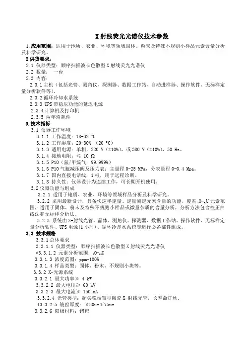
X射线荧光光谱仪技术参数1.应用范围:适用于地质、农业、环境等领域固体、粉末及特殊不规则小样品元素含量分析及科学研究。
2供货要求:2.1仪器类型:顺序扫描波长色散型X射线荧光光谱仪2.2数量:一台2.3内容:2.3.1主机(包括光管、测角仪、探测器、数据工作站、自动进样器、操作软件、无标样定量分析软件等)。
2.3.2循环冷却水系统2.3.3UPS带稳压功能的延迟电源2.3.4计算机及打印机2.3.5两年消耗件3.技术指标3.1仪器工作环境3.1.1工作温度:18-32︒C3.1.2工作湿度:20-80%(20︒C)3.1.3适用电源:单相,220V(±10%),或380V(±10%),50Hz。
3.1.4接地电阻:≤10Ω3.1.5P10(氩/甲烷气:99.999%)3.1.6P10气瓶减压阀及压力表:主量程0-25MPa,分表量程0-0.4Mpa。
3.1.7国内直拨电话线:1根,用于远程诊断。
3.1.8持久性:仪器设计为连续工作,可长期开机使用。
3.2仪器功能与组成3.2.1适用于地质、农业、环境等领域样品分析及科学研究。
3.2.2采用最新设计,具备快速半定量、定量测定元素含量的功能,覆盖8O-92U元素范围,适用于固体、粉末及特殊不规则小样品或微量杂质的含量分析,分析方法包含校正曲线法和无标样分析法。
3.2.3系统由X-射线光管、晶体、测角仪、探测器、数据工作站、操作软件、无标样定量分析软件、UPS电源(1小时)、循环冷却水系统等运行必备部件组成。
3.3技术规格3.3.1总体要求3.3.1.1仪器类型:顺序扫描波长色散型X射线荧光光谱仪*3.3.1.2元素分析范围:8O-92U3.3.1.3浓度范围:ppm-100%3.3.1.4样品类型:固体、粉末、不规则小块等。
3.3.2X-光源系统3.3.2.1最大功率≥4kW3.3.2.2最大电压≥60kV3.3.2.3最大电流≥150mA3.3.2.4光管类型:超尖锐端窗型陶瓷X-射线光管,长寿命灯丝。
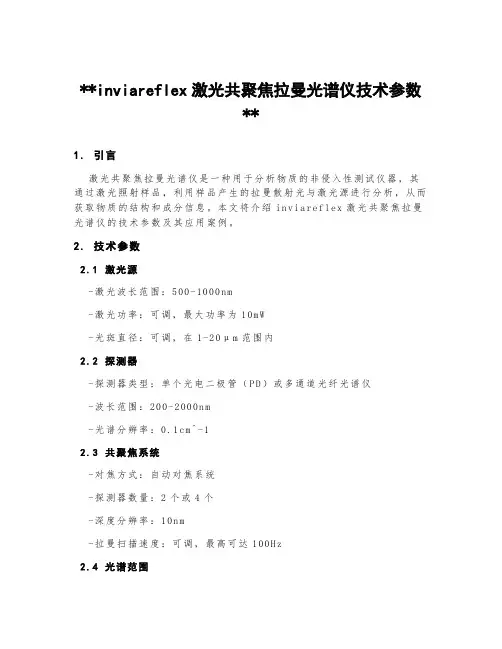
**inviareflex激光共聚焦拉曼光谱仪技术参数**1.引言激光共聚焦拉曼光谱仪是一种用于分析物质的非侵入性测试仪器,其通过激光照射样品,利用样品产生的拉曼散射光与激光源进行分析,从而获取物质的结构和成分信息。
本文将介绍i nv ia re fl ex激光共聚焦拉曼光谱仪的技术参数及其应用案例。
2.技术参数2.1激光源-激光波长范围:500-1000nm-激光功率:可调,最大功率为10m W-光斑直径:可调,在1-20μm范围内2.2探测器-探测器类型:单个光电二极管(P D)或多通道光纤光谱仪-波长范围:200-2000nm-光谱分辨率:0.1cm^-12.3共聚焦系统-对焦方式:自动对焦系统-探测器数量:2个或4个-深度分辨率:10n m-拉曼扫描速度:可调,最高可达100H z2.4光谱范围-拉曼频移范围:100-4000cm^-1-光谱采集范围:可选,常见为1000-3500c m^-12.5样品台-样品台类型:X YZ扫描台-X Y平移范围:10mm×10mm-Z轴扫描范围:2m m3.应用案例3.1药物研发i n vi ar ef lex激光共聚焦拉曼光谱仪在药物研发领域发挥着重要作用。
通过对药物的拉曼光谱进行分析,可以实时监测药物的成分、结构和形态变化,提高药物的质量控制和生产效率。
3.2材料科学在材料科学领域,in v ia re fl ex激光共聚焦拉曼光谱仪可用于研究材料的晶体结构、表面形貌以及材料中的缺陷等性质。
通过拉曼光谱的分析,可以实现对材料性能和制备工艺的优化,提高材料的性能和稳定性。
3.3生物医学i n vi ar ef le x激光共聚焦拉曼光谱仪在生物医学领域有广泛的应用。
它可以用于细胞和组织的非侵入性分析,帮助研究人员了解细胞的化学组成、病变及代谢状态。
此外,激光共聚焦拉曼光谱仪还可用于生物标记物的鉴定和肿瘤诊断。
结论i n vi ar ef le x激光共聚焦拉曼光谱仪凭借其优秀的技术参数和广泛的应用领域,成为物质分析和研究领域的重要工具之一。
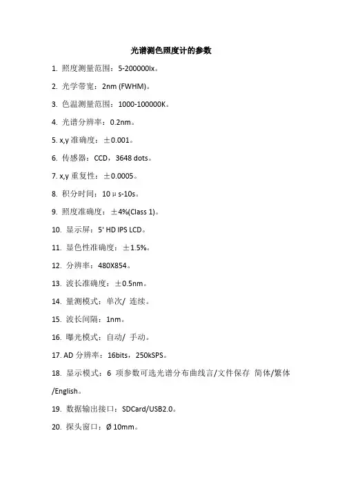
光谱测色照度计的参数1. 照度测量范围:5-200000lx。
2. 光学带宽:2nm (FWHM)。
3. 色温测量范围:1000-100000K。
4. 光谱分辨率:0.2nm。
5. x,y准确度:±0.001。
6. 传感器:CCD,3648 dots。
7. x,y重复性:±0.0005。
8. 积分时间:10μs-10s。
9. 照度准确度:±4%(Class 1)。
10. 显示屏:5' HD IPS LCD。
11. 显色性准确度:±1.5%。
12. 分辨率:480X854。
13. 波长准确度:±0.5nm。
14. 量测模式:单次/ 连续。
15. 波长间隔:1nm。
16. 曝光模式:自动/ 手动。
17. AD分辨率:16bits,250kSPS。
18. 显示模式:6项参数可选光谱分布曲线言/文件保存简体/繁体/English。
19. 数据输出接口:SDCard/USB2.0。
20. 探头窗口:Ø 10mm。
21. 尺寸(L x W x H):163x81x25.8mm。
光谱测色照度计的功能包括相关色温Tc(K)、黑体偏离Duv、光照度E(lx)、烛光E(Fc)、辐射照度Ee(W/m²)、色品坐标(x,y)、(u,v)、(u',v')、相对光谱功率分布P(λ)、显色指数Ra,Ri(i=1~15)、色品坐标图CIE1976 CIE1960 CIE1931、色容差图SDCM(麦克亚当椭圆、矩形框以及CIEu’v’圆)、主波长、峰值波长、中心波长、质心波长、半宽度、明暗视觉比S/P、色纯度、红色比、绿色比、蓝色比,CIE1931三基色刺激值X、Y、Z等。

光谱仪重要参数范文光谱仪是一种用于测量光波的仪器,可以将光波分解成其组成的不同波长,并进一步分析和测量其强度。
光谱仪常被广泛应用于物理学、化学、生物学、天文学等领域。
在光谱仪中,有一些重要的参数需要考虑,下面将对这些参数进行详细介绍。
1.分辨率:光谱仪的分辨率是指其区分能力,即能够分辨两个非常接近的波长之间的差异。
对于光谱仪而言,分辨率越高,就越能够分辨出光谱中不同波长的组成部分。
分辨率通常用波长间的最小差异来表示,可以通过改变光谱仪的设计、光栅或光学系统来调整分辨率。
2.灵敏度:光谱仪的灵敏度是指其检测能力,即能够检测到非常弱的光信号。
光谱仪的灵敏度可以通过改变光学元件、探测器以及放大电路来改善。
3.动态范围:光谱仪的动态范围是指其能够测量的最弱和最强光信号之间的差异范围。
动态范围的大小决定了光谱仪可以测量的强度范围。
较大的动态范围可以提供更准确的测量结果,特别是在涉及到强信号和弱信号同时存在的情况下。
4.波长范围:光谱仪的波长范围是指其能够测量的光信号的波长范围。
不同领域中可能需要测量不同波长范围的光信号,因此选择合适的波长范围对于光谱仪的应用非常重要。
波长范围通常由选择不同的光学元件或探测器来确定。
5.稳定性:光谱仪的稳定性是指其测量的重复性和长期稳定性。
稳定性对于进行精确的测量和比较非常重要。
不同因素如温度、湿度和光路的稳定性都会对光谱仪的性能产生影响。
因此,提高光谱仪的稳定性需要考虑这些因素,并进行相应的校准和维护。
6.采样速率:光谱仪的采样速率是指它能够对光信号进行采样和处理的速度。
较高的采样速率意味着能够更快地获取到光信号的分析结果,特别是在实时应用和快速变化的光信号测量中非常重要。
除了上述参数外,还有其他可能的重要参数,如光谱仪的重量、体积、功率消耗等。
这些参数与实际应用中的需求和限制相关,需要根据具体情况进行考虑和选择。
此外,光谱仪的成本也是一个重要的因素。
总之,光谱仪的重要参数需要综合考虑,以满足特定的应用需求。
一、荧光光谱仪的原理和应用荧光光谱仪是一种用于测量物质荧光发射光谱的仪器。
它利用物质受到紫外或可见光激发后发出的荧光来进行分析和检测。
荧光光谱仪广泛应用于生物医药、环境监测、食品安全等领域,具有灵敏度高、分辨率好、快速准确等特点。
二、荧光光谱仪的参数和规格1. 光源:荧光光谱仪一般采用氙灯或汞灯作为激发光源,氙灯的波长范围广,能够提供较强的激发光,而汞灯则具有比较稳定的输出功率。
2. 分光器:荧光光谱仪的分光器通常采用全息光栅或单色器,能够对荧光光谱进行高效分光和检测。
全息光栅具有分辨率高、光谱范围宽的优点,而单色器则能够提供较高的光谱分辨率。
3. 探测器:荧光光谱仪的探测器一般采用光电二极管(PMT)或光电倍增管(PMT)进行荧光信号的检测和转换。
PMT具有灵敏度高、响应速度快的特点,但对环境要求较高;而PMT则可适用于较恶劣的环境条件下。
4. 光谱范围:荧光光谱仪的光谱范围通常覆盖200-800nm,不同型号的荧光光谱仪具有不同的光谱范围和分辨率。
5. 数据处理系统:现代荧光光谱仪通常配备有先进的数据处理系统,能够实现数据采集、分析和报告输出等功能,提高了检测的自动化程度和准确性。
6. 标定和验证:荧光光谱仪的参数需要经过定期的标定和验证,以确保其检测结果的准确性和可靠性。
三、荧光光谱仪的操作和维护1. 操作:使用荧光光谱仪时,应严格按照操作手册的要求进行操作,保证仪器正常工作。
在操作过程中,应注意仪器的稳定性和光路的清洁,避免外界光线的干扰。
2. 维护:定期对荧光光谱仪进行维护保养,清洁光路和探测器,定期更换光源等关键部件,保证仪器的稳定性和准确性。
四、荧光光谱仪的应用荧光光谱仪在生物医药领域广泛应用于蛋白质、核酸、细胞等生物分子的检测和定量分析;在环境监测领域可以用于水质和大气等环境样品的有机物和金属离子的检测;在食品安全领域可用于食品中有毒物质和添加剂的分析等。
五、总结荧光光谱仪作为一种先进的分析仪器,具有灵敏度高、分辨率好、快速准确等特点,广泛应用于生物医药、环境监测、食品安全等领域。
cs2000a光谱仪使用指导书一、简介1.1仪器概述c s2000a光谱仪是一款高精度的光学测量仪器,广泛应用于颜色测量、光谱分析等领域。
本文档将详细介绍c s2000a光谱仪的使用方法和操作步骤,帮助用户快速掌握该仪器的使用技巧。
1.2适用范围本文档适用于所有使用c s2000a光谱仪的用户,包括初学者和有一定经验的用户。
对于初学者,我们将从基本操作开始介绍;对于有经验的用户,我们将提供更高级的功能和应用技巧。
二、仪器准备2.1连接电源首先,将cs2000a光谱仪插入电源插座,并确保电源线与仪器连接牢固。
接下来,打开电源开关,待仪器启动完成后,屏幕上将显示出c s2000a的主界面。
2.2连接计算机c s2000a光谱仪可以通过U SB接口与计算机进行连接。
使用附带的U S B数据线将光谱仪与计算机相连,并确保连接稳固。
此时,计算机将自动识别到cs2000a光谱仪,并安装相关驱动程序。
三、仪器操作3.1主界面介绍c s2000a光谱仪的主界面分为三大部分:菜单栏、测量参数设置区和测量结果显示区。
菜单栏包含了各项功能和设置选项,用户可以通过菜单栏进行相关操作;测量参数设置区用于设置测量所需的参数,如光源类型、波长范围等;测量结果显示区将实时显示测量结果。
3.2测量步骤步骤一:选择光源类型点击菜单栏中的“光源”选项,选择合适的光源类型,常见的光源类型有“A型”、“D50”、“D65”等。
步骤二:设置波长范围点击菜单栏中的“波长”选项,设置所需的波长范围。
根据具体的测量需求,可以选择设置单一波长或连续波长范围。
步骤三:进行测量在测量参数设置区域输入相关测量参数后,点击菜单栏中的“开始测量”按钮,c s2000a光谱仪将开始进行光谱测量。
测量结果将实时显示在测量结果显示区域。
步骤四:保存测量数据在完成测量后,点击菜单栏中的“保存数据”选项,选择保存路径和文件名,将测量结果保存到计算机中。
3.3测量技巧光源选择-不同光源类型适用于不同的应用场景,根据具体需要选择合适的光源类型,以获得准确的测量结果。
拉曼光谱仪参数设置拉曼光谱仪是一种非常重要的分析仪器,它可以通过激发样品中的分子振动,获得样品特殊的拉曼光谱,进而用于研究分子的结构和组成。
而在进行样品的分析和研究时,拉曼光谱仪参数设置的优与不优,往往会直接影响到测试结果的质量和可靠性。
下面就来详细介绍一下拉曼光谱仪参数设置的相关信息。
一、激光源拉曼光谱仪的激光源通常采用Nd:YAG激光或者氦氖激光。
在选择激光源时,需要考虑激光的波长和功率。
通常情况下,Nd:YAG激光的波长为1064nm,而氦氖激光的波长为632.8nm。
在选择激光功率时,通常需要根据样品的特性和要求进行选择。
二、样品台样品台的稳定性非常重要,因为任何的震动和位移都会对测试结果产生很大的影响。
拉曼光谱仪的样品台通常采用先进的技术,以保证稳定性和可靠性。
同时,样品台还应该具有可调节的X、Y、Z三个方向的调整能力。
三、光谱仪分辨率光谱仪分辨率会影响到拉曼光谱的谱线宽度和分布情况。
通常情况下,光谱仪的分辨率越高,拉曼光谱的分辨率越高,同时峰值也会更加尖锐。
在实际使用中,可以通过减小孔径的尺寸和增加光栅刻线来提高光谱仪的分辨率。
四、光收集系统光收集系统负责将激光散射回来的光收集到探测器中,因此其构造和设计都应该尽量避免光的散射和漏光。
在实际应用中,可以通过采用光纤耦合、光栅和透镜来进一步优化光收集系统。
五、探测器探测器是整个拉曼光谱仪系统中最为关键的部件之一,它能够将拉曼光谱通过电信号转化成可视化数据。
目前市场上有很多种不同的探测器可供选择,例如光电二极管探测器、CCD探测器等。
在选择探测器时,需要考虑其响应速度、量子效率和暗噪声等性能参数。
通过上述五个方面来分析,我们可以发现,拉曼光谱仪参数设置的影响因素非常多,需要细心和耐心地进行考虑和选择。
只有对每个参数的设置都进行了恰当的调整和优化,才能得到更为准确可靠的测试结果,进一步满足实际应用需求。
国产深圳荧光光谱仪技术参数
以下是一些可能的技术参数,具体规格取决于制造商和型号:
- 光源:氙灯或氩气离子激光
- 波长范围:200-900 nm 或更广泛
- 分辨率:通常为0.1-1 nm
- 灵敏度:通常为ppm或ppb级别
- 光程:通常为10-100 mm
- 探测器:光电倍增管、CCD阵列或PMT等
- 样品室:单样品池或多样品盘
- 聚焦系统:可能有自动聚焦或手动聚焦功能
- 控制软件:可以基于Windows或者Linux系统
- 其他功能:比如多种激发方式、时间分辨、温度控制、样品旋转等
需要注意的是,荧光光谱仪是一种非常复杂的仪器,不仅需要可靠的技术参数,还需要良好的仪器性能和使用体验,以及适合用户的软件界面和支持。
光谱关键参数光谱的关键参数主要包括以下几个方面:1.光谱范围:指光源所发射的光的波长范围。
对于连续光谱灯,如氢灯、氘灯、白炽灯等,它们的光谱范围是某一较长波段的光辐射。
例如,氢灯与氘灯的光谱范围为180~400nm,白炽灯为330~800nm。
而对于超连续谱光源,如SC-5,其光谱范围可以从470nm到2400nm。
2.功率与功率谱密度:功率是指光源发射光的总能量,通常以瓦特(W)为单位。
功率谱密度则描述了光源在单位波长范围内的功率分布,通常以W/nm或dBm/nm为单位。
例如,SC-5超连续谱光源的总输出功率大于800mW,功率谱密度在800-1700nm范围内大于-10dBm/nm。
3.光谱稳定性:描述了光源在长时间工作或在不同环境条件下光谱特性的变化程度。
光谱稳定性通常以百分比或分贝(dB)表示。
例如,SC-5超连续谱光源在800-1700nm 范围内的光谱稳定性小于0.1dB。
4.偏振状态:描述了光源发射光的电场矢量的振动方向。
偏振状态可以影响光与物质的相互作用,因此在某些应用中需要特定的偏振状态。
5.重复频率和脉宽:对于脉冲光源,重复频率和脉宽是两个重要参数。
重复频率描述了每秒钟光源发射的脉冲数量,而脉宽则描述了单个脉冲的持续时间。
6.光束质量:描述了光源发射光的空间分布特性。
光束质量通常以M²因子表示,它描述了光束的聚焦能力和传输性能。
请注意,这些参数并不是孤立的,它们之间相互关联并共同决定了光源的性能和应用范围。
在选择光源时,需要根据具体的应用需求和实验条件来综合考虑这些参数。
Devices (CCD) Arrays and Photo Diode (PD) Arrays, enabled the production of low cost scanners, CCD cameras etc. The same CCD and PDA detectors are now used in the Avantes line of spectrometers, enabling fast scanning of the spectrum, wit-hout the need of a moving grating.Thanks to the need for fiber optics in the communication technology, low absorption silica fibers have been developed. Similar fibers can be used as measurement fibers to transport light from the sample to the optical bench of the spectrome-ter. The easy coupling of fibers allows a modular build-up of a system that consists of light source, sampling accessories and fiber optic spectrometer.Advantages of fiber optic spectroscopy are the modularity and flexibility of the system. The speed of measurement allows in-line analysis, and the use of low-cost commonly used detectors enable a complete low cost Avantes spectrometer system.Optical spectroscopy is a technique for measuring light intensity in the UV-, VIS-, NIR- and IR-region. Spectroscopic measurements are being used in many different applications, such as color measurement, concentration determination of chemical components or electromagnetic radiation analysis. For more elaborate application information and setups, please see further the Application chapter at the end of this catalog.A spectroscopic instrument generally consists of entrance slit, collimator, a dispersive element, such as a grating or prism, focusing optics and detector. In a monochromator system there is normally also an exit slit, and only a narrow portion of the spectrum is projected on a one-element detector. In monochromators the entrance and exit slits are in a fixed position and can be changed in width. Rotating the grating scans the spectrum.Development of micro-electronics during the 90’s in the field of multi-element optical detectors, such as Charged Coupledmetrical Czerny-Turner design (figure 1).Light enters the optical bench through a standardSMA905 connector and is collimated by a spherical mirror. A plane grating diffracts the collimated light; a second spherical mirror focuses the resulting diffracted light. An image of the spectrum is projected onto a 1-dimensional linear detector array.installed configurations, depending on the intended application. The choice of these components such as the diffraction grating, entrance slit, order sorting filter, and detector coating have a strong influence on system specifications. Sensitivity, resolution, bandwidth and stray light are further discussed in the following paragraphs.Introduction Fiber Optic SpectroscopySpectrometersinfo@ • S p e c t r o m e t e r s •info@Biomedical Technology Chemistry Colorimetry Food Technology Inline Process Control Radiometry Thinfilm AnalysisHow to configure a spectrometer for your application?For optimal UV sensitivity we recommend the back-thinned UV sensitive CCD detector, as implemented in the AvaSpec-2048x14.For the different detector types the photometric sensitivity is given in table 4, the spectral sensitivity for each detector is depicted in figure 5.b. Chemometric SensitivityTo detect two absorbance values, close to each other with maximum sensitivity you need a high Signal to Noise (S/N) performance. The detector with best S/N performance is the 2048x14 pixel back-thinned CCD detector, next to the 256/1024 CMOS detector in the AvaSpec-256/1024. The S/N performance can also be enhanced by averaging over multiple spectra.4. Timing and SpeedThe data capture process is inherently fast with detector arrays and no moving parts. However there is an optimal detector for each application. For fast response applications, we recommend to use the AvaSpec- USB2 platform spectrometers. When datatransfer time is critical we recommend to select a small amount of pixels to be transferred with the UBS2 interface. Data transfer time can be enhanced by selecting the pixel range of interest to be transmitted to the PC; in general the AvaSpec-128 may be considered as the fastest spectrometer with more than 8000 scans per second.The above parameters are the most important in choosing the right spectrometer configuration, please contact our application engi-neers to optimize and fine-tune the system to your needs. On the next page you will find a quick reference table 1 for most common applications, for a more elaborate explanation and configurations, please refer to the applications section in the back of this catalog.In addition we have introduced in this catalog application icons, that will help you to find the right products and accessories for your applications.In the modular AvaSpec design a number of choices have to be made on several optical components and options, depending on the application you want to use the spectrometer for.This section should give you some guidance on how to choose the right grating, slit, detector and other options, installed in the AvaSpec.1. Wavelength RangeIn the determination for the optimal configuration of a spectrometer system the wavelength range is the first important parameter that defines the grating choice. If you are looking for a wide wavelength range, we recommend to take an A-type (300 lines/mm) or B-type (600 lines/mm) grating (see Grating selection table in the spectrometer product section). The other important component is the detector choice, Avantes offers 9 different detector types with each different sensitivity curves (see figure 5). For UV applications the new 2048x14 pixel back-thinned CCD detector, the 256/1024 pixel CMOS detectors or DUV- enhanced 2048 or 3648 pixel CCD detectors may be selected. For the NIR range 3 different InGaAs detectors are available.If you want to combine a wide range with a high resolu-tion, a multiple channel spectrometer may be the best choice.2. Optical ResolutionIf you desire a high optical resolution we recommend to pick a grating that has 1200 or more lines/mm (C,D,E or F types) in combination with a narrow slit and a detector with 2048 or 3648 pixels, for example 10 µm slit for the best resolution on the AvaSpec-2048 (see Resolution table in the spectrometer product section)3. SensitivityTalking about sensitivity, it is very important to distinguish between photometric sensitivity (How much light do I need for a detectable signal?) and chemometric sensitivity (What absorbance difference level can still be detected?) a. Photometric SensitivityIn order to achieve the most sensitive spectrometer in for example Fluorescence or Raman applications we recommend the 2048 pixel CCD detector, as in the AvaSpec-2048. Further we recommend the use of a DCL-UV/VIS detector collection lens, a relatively wide slit (100µm or wider) or no slit and an A type grating. For an A-type grating (300 lines/mm) the light dispersion is minimal, so it has the highest sensitivity of the grating types. Optionally the Thermo-electric cooling of the CCD detector (see product section AvaSpec-2048-TEC, page 30) may be chosen to minimize noise and increase dynamicrange at long integration times (60 seconds).Table 1 Quick reference guide for spectrometer configurationApplication AvaSpec- Grating WL range (nm) Coating SlitFWHM DCL OSF OSCtype Resolution (nm)Biomedical 2048 NB 500-1000 - 50 1.2 - 475 -Chemometry 1024 UA 200-1100 - 50 2.0 - - OSC-UA 128 VA 360-780 - 100 6.4 X/- - -Color 256 VA 360-780 - 50 3.2 - - -2048 BB 360-780 - 200 4.1 X/- - -Fluorescence 2048 VA 350-1100 - 200 8.0 X - OSC Fruit-sugar 128 IA 800-1100 - 50 5.4 X 600 -Gemology 2048 VA 350-1100 - 25 1.4 X - OSC High 2048 VD 600-700 - 10 0.07 - 550 -resolution 3648 VD 600-700 - 10 0.05 - 550 -High UV- 2048x14UC200-450-2002.0---Sensitivity Irradiance 2048 UA 200-1100 DUV 50 2.8 X/- - OSC-UA Laserdiode 2048 NC 700-800 - 10 0.1 - 600 -LED 2048 VA 350-1100 - 25 1.4 X/- - OSC LIBS 2048FT UE 200-300 DUV 10 0.09 - - - 2048USB2 UE 200-300 DUV 10 0.09 - - -Raman 2048TEC NC 780-930 - 25 0.2 X 600 -Thin Films 2048 UA 200-1100 DUV - 4.1 X - OSC-UA UV/VIS/NIR 2048 UA 200-1100 DUV 25 1.4 X/- - OSC-UA 2048x14UA200-1100 - 25 1.4 - - OSC-UA NIR NIR256-1.7 NIRA 900-1750 - 50 5.0 - 1000 - NIR256-2.2 NIRZ 1200-2200 - 50 10.0 - 1000 -NIR256-2.5 NIRY1000-2500-5015.0-1000-info@ • Spectrometers9S p e c t r o m e t e r s • info@For each spectrometer type, a grating selection table is shown in the Spectrometer Platforms section. Table 2 illustrates how to read the grating selection table. The spectral range to select in Table 2 depends on the starting wavelength of the grating Please select Spectral range band-width from the useable Wavelength range, for example: grating UE (200-315nm)*the spectral range depends on the starting wavelength of the grating; the higher the wave-length, the smaller the range.For example grating UE (510-580 nm)The order code is defined by 2 letters: the first is the Blaze (U= 250/300nm or UV for holo-graphic, B=400nm, V=500nm or VIS for holo-graphic, N=750nm, I=1000nm) and the second the nr of lines/mm (Z=150, A=300, B=600, C=1200, D=1800, E=2400, F=3600 lines/mm)Spectrometersinfo@ •Figure 2 Grating Efficiency Curves 300 Lines/mm Gratings600 Lines/mm Gratings1200 Lines/mm Gratings 1800 Lines/mm Gratings2400 Lines/mm Gratings3600 Lines/mm GratingsSpectrometers •info@Figure 3 Grating Dispersion Curves300 Lines/mm Gratings600 Lines/mm Gratings1200 Lines/mm Gratings1800 Lines/mm Gratings2400 Lines/mm Gratings3600 Lines/mm Gratingsinfo@ •SpectrometersThe optical resolution is defined as the minimum difference in wavelength that can be separated by the spectrometer. For separation of two spectral lines it is necessary to image them at least 2 array-pixels apart. Because the grating determines how far different wavelengths are separated (dispersed) at the detector array, it is an important variable for the resolution.The other important parameter is the width of the light beam entering the spectrometer. This is basically the instal-led fixed entrance slit in the spectrometer, or the fiber core diameter when no slit is installed.The slits can be installed with following dimensions: 10, 25 or 50 x 1000 µm high or 100, 200 or 500 µm x 2000 µm high. Its image on the detector array for a given wavelength will cover a number of pixels. For two spectral lines to be separated, it is now necessary that they be dispersed over at least this image size plus one pixel. When large core fibers are used the resoluti-on can be improved by a slit of smaller size than the fiber core. This effectively reduces the width of the entering light beam. The influence of the chosen grating and the effective width of the light beam (fiber core or entrance slit) are shown in the tables at the product information. In Table 3 the typical reso-lution can be found for the AvaSpec-2048. Please note that for the higher lines/mm gratings the pixel dispersion varies along the wavelength range and gets better towards the lon-ger wavelengths (see also Figure 3). The best resolution can always be found for the longest wavelengths. The resolution in this table is defined as F(ull) W(idth) H(alf) M(aximum), which is defined as the width in nm of the peak at 50% of the maximum intensity (see Figure 4).Graphs with information about the pixel dispersion can be found in the gratings section as well, so you can optimally determine the right grating and resolution for your specific application.In combination with a DCL-detector collection lens or thick fibers the actual FWHM value can be 10-20% higher than the value in the table. For best resolution small fibers and no DCLFigure 4 Full Width Half MaximumHow to select optimal Optical Resolution?Slit size (µm)Grating (lines/mm) 10 25 50 100 200 500 300 0.8 1.4 2.4 4.3 8.0 20.0600 0.4 0.7 1.2 2.1 4.1 10.01200 0.1-0.2* 0.2-0.3* 0.4-0.6* 0.7-1.0* 1.4-2.0* 3.3-4.8*1800 0.07-0.12* 0.12-0.21* 0.2-0.36* 0.4-0.7* 0.7-1.4* 1.7-3.3*2400 0.05-0.09* 0.08-0.15* 0.14-0.25* 0.3-0.5* 0.5-0.9* 1.2-2.2*36000.04-0.06*0.07-0.10*0.11-0.16*0.2-0.3*0.4-0.6*0.9-1.4**depends on the starting wavelength of the grating; the higher the wavelength, the bigger the dispersion and the better the resolutionTable 3 Resolution (FWHM in nm) for the AvaSpec-2048Installed Slit in SMA AdapterS p e c t r o m e t e r s •info@The AvaSpec spectrometers can be equipped with several types of detector arrays. Presently we offer silicon-based CCD, back-thinned CCD, CMOS and Photo Diode Arrays for the 200-1100 nm range. A complete overview is given in the next sec-tion “Sensitivity” in table 4. For the NIR range (1000-2500nm) InGaAs arrays are implemented.CCD Detectors (AvaSpec-2048/3648)The Charged Coupled Device (CCD) detector stores the charge, dissipated as photons strike the photoactive surface. At the end of a controlled time-interval (integration time), the remaining charge is transferred to a buffer and then this signal is being transferred to the AD converter. CCD detectors are naturally integrating and therefore have an enormous dynamic range, only limited by the dark (thermal) current and the speed of the AD converter. The 3648 pixel CCD has an integrated electronic shutter function, so an integration time of 10µsec can be achieved.+ Advantages for the CCD detector are many pixels (2048 or 3648), high sensitivity and high speed.- Main disadvantage is the lower S/N ratio.UV enhancementFor applications below 350 nm with the AvaSpec-2048/3648 a special DUV-detector coating is required. The uncoated CCD-response below 350 nm is very poor; the DUV lumo-gen coating enhances the detector response in the region 150-350nm. The DUV coating has a very fast decay time, typ. in ns range and is therefore useful for fast trigger LIBS applications.Back-thinned CCD Detectors (AvaSpec-2048x14)For applications requiring high quantum efficiency in the UV (200-350nm) and NIR (900-1160nm) range, combined with good S/N and a wide dynamic range, the new back-thinned CCD detector may be the right choice. The detector is an area detector of 2048x14 pixels, for which the vertical 14 pixels are binned (electronically added together) to have more sensiti-vity and a better S/N performance. + A dvantage of the back-thinned CCD detector is the good UV and NIR sensitivity, combined with good S/N and dynamic range- Disadvantage is the relative high costPhoto Diode Arrays (AvaSpec-128)A silicon photodiode array consists of a linear array of mul-tiple photo diode elements, for the AvaSpec-128 this is 128 pixels. Each pixel consists of a P/N junction with a positively doped P region and a negatively doped N region. When light enters the photodiode, electrons will become excited and output an electrical signal. Most photodiode arrays have anDetector Arraysintegrated signal processing circuit with readout/integration amplifier on the same chip.+ Advantages for the Photodiode detector are high NIR sensitivity and high speed.- Disadvantages are limited amount of pixels and no UV response.CMOS linear image sensors (AvaSpec-256/1024)These so called CMOS linear image sensors have a lower charge to voltage conversion efficiency than CCD array sensors and are therefore less light sensitive, but have a much better signal to noise ratio.The CMOS detectors have a higher conversion gain than NMOS detectors and also have a clamp circuit added to the internal readout circuit to suppress noise to a low level.+ Advantages for the CMOS detectors are good S/N ratio and good UV sensitivity.- Disadvantages are the low readout speed, low sensitivity, and relative high cost (1024 pixels).InGaAs linear image sensors (AvaSpec-NIR256)The InGaAs linear image sensors deliver high sensitivity in the NIR wavelength range. The detector consists of a charge ampli-fier array with CMOS transistors, a shift register and timing generator. 3 versions of detectors are available:• 256 pixel non-cooled InGaAs detector for the 900-1750nm useable range • 256 pixel 2-stage cooled Extended InGaAs detector for the 1000-2200nm range • 256 pixel 2-stage cooled Extended InGaAs detector for the1000-2500nm rangeDifferent Detector ArraysSensitivityThe sensitivity of a detector pixel at a certain wavelength is defined as the detector electrical output per unit of radia-tion energy (photons) incident to that pixel. With a given A/D converter this can be expressed as the number of counts per mJ of incident radiation.The relation between light energy entering the optical bench and the amount hitting a single detector pixel depends on the optical bench configuration. The efficiency curve of the grating used, the size of the input fiber or slit, the mirror performance and the use of a Detector Collection Lens are the main parameters. With a given set-up it is possible to do measurements over about 6-7 decades of irradiance levels. Some standard detector specifications can be found in Table 4 detector specifications. Optionally a cylindrical Detector Collection Lens (DCL) can be mounted directly on the detec-tor array. The quartz lens (DCL-UV for AvaSpec-2048/3648) will increase the system sensitivity by a factor of 3-5, depen-ding on the fiber diameter used.In Table 4 the overall sensitivity is given for the detector types currently used in the UV/VIS AvaSpec spectrometers as output in counts per ms integration time for a 16-bit AD converter. To compare the different detector arrays we have assumed an optical bench with 600 lines/mm grating and no DCL. The entrance of the bench is an 8 µm core diameter fiber, con-nected to a standard AvaLight-HAL halogen light source. This is equivalent to ca. 1 µWatt light energy input.In table 5 the specification is given for the NIR spectrometers, in figure 5 and figure 6 the spectral response curve for the dif-ferent detector types are depicted.info@ •SpectrometersTable 4 Detector specifications (based on a 16-bit AD converter)Detector TAOS 128 HAM256 HAM1024 SONY2048 TOSHIBA3648 HAM2048x14Type Photo diode array CMOS linear array CMOS linear array CCD linear array CCD linear array Back-thinnedCCD Array # Pixels, pitch 128, 63.5 µm 256, 25 µm 1024, 25 µm 2048, 14 µm 3648, 8 µm 2048x14, 14 µmpixel width x 55.5 x 63.5 25 x 500 25 x 500 14 x 56 8 x 200 14x14 (totalheight (µm)height 196 µm)pixel well depth 250,000 4,000,000 4,000,000 40,000 120,000 250,000(electrons)Sensitivity 100 22 22 240 160 200V/lx.sSensitivity 100 440 440 40 60 50Photons/count@600nmSensitivity 4000 120 120 20,000 14,000 16,000(AvaLight-HAL, (AvaSpec-128) (AvaSpec-256) (AvaSpec-1024) (AvaSpec-2048) (AvaSpec-3648) (Avaspec 2048x14)8 µm fiber)in counts/µW perms integration timePeak wavelength 750 nm 500 nm 500 nm 500 nm 550 nm 650 nmSignal/Noise 500:1 2000 :1 2000 :1 200 :1 350 :1 500:1Dark noise 60 28 60 35 35 50(counts RMS)Dynamic Range 1000 2500 2500 2000 2000 1300PRNU**± 4% ± 3% ±3% ± 5% ± 5% ± 3%Wavelength range 360-1100 200-1000 200-1000 200*-1100 200*-1100 200-1160(nm)Frequency 2 MHz 500 kHz 500 kHz 2 MHz 1 MHz 1.5 MHz* DUV coated** Photo Response Non-Uniformity = max difference between output of pixels when uniformly illuminated, divided by average signalS p e c t r o m e t e r s • info@Figure 5 Detector Spectral sensitivity curves Table 5 NIR Detector SpecificationsDetectorNIR256-1.7 NIR256-2.2NIR256-2.5TypeLinear InGaAs array Linear InGaAs array Linear InGaAs arraywith 2 stage TE cooling with 2 stage TE cooling # Pixels, pitch 256, 50 µm 256, 50 µm 256, 50 µm pixel width x 50 x 50050 x 500 50 x 500height (µm)Pixel well depth 16,000,000 1,500,000 1,500,000(electrons)Sensitivity 350250200(AvaLight-HAL, 8 µm fiber)in counts/µW per ms integration timePeak wavelength 1550 nm 2000 nm 2300 nmSignal/Noise 4000:1 1200 :1 1200 :1Dark noise 12 40 40 (counts RMS)Dynamic Range 5000 1600 1600PRNU** ± 5% ± 5% ± 5%Defective pixels 012 12(max)Wavelength range 900-1750 1000-2200 1000-2500 (nm)Frequency500 kHz500 kHz500 kHz** Photo Response Non-Uniformity = max difference between output of pixels when uniformly illuminated, divided by average signalFigure 6 NIR Detector Sensitivity CurvesSpectrometers Stray light is radiation of the wrong wavelength that activatesa signal at a detector element. Sources of stray light can be:• Ambient light• Scattering light from imperfect optical components orreflections of non-optical components• Order overlapEncasing the spectrometer in a light tight housing eliminatesambient stray light.When working at the detection limit of the spectrometersystem, the stray light level from the optical bench, gratingand focusing mirrors will determine the ultimate limit ofdetection. Most gratings used are holographic gratings,known for their low level of stray light. Stray light measure-ments are being carried out with a laser light, shining into theoptical bench and measuring light intensity at pixels far awayfrom the laser projected beam. Other methods use a halogenlight source and long pass- or band pass filters.Typical stray light performance is <0.05 % at 600 nm; <0.10% at 435 nm; <0.10 % at 250 nm.Second order effects, which can play an important role forgratings with low groove frequency and therefore a widewavelength range, are usually caused by the grating 2ndorder diffracted beam. The effects of these higher orders canoften be ignored, but sometimes need to be taken care of.The strategy is to limit the light to the region of the spectra,where order overlap is not possible. Second order effectscan be filtered out, using a permanently installed long-passoptical filter in the SMA entrance connector or an order sor-ting coating on a window in front of the detector. The ordersorting coatings on the window typically have one long passfilter (590nm) or 2 long pass filters (350 nm and 590 nm),depending on the type and range of the selected grating.In Table 6 a wide range of optical filters for installation in theoptical bench can be found. The use of following long-passfilters is recommended: OSF-475 for grating NB and NC, OSF-515/550 for grating NB and OSF-600 for grating IB.In addition to the order sorting coatings we implement partialDUV coatings on Sony 2048 and Toshiba 3648 detectors toavoid second order effects from UV response and to enhancesensitivity and decrease noise in the Visible range.This partial DUV coating is done automatically for the follo-wing grating types:• UA for 200-1100 nm, DUV400, only first 400 pixelscoated• UB for 200-700 nm, DUV800, only first 800 pixelscoatedStray Light and Second Order EffectsTable 6 Filters installed in the AvaSpec spectrometer seriesOSF-385Permanently installed 1 mm order sorting filter @ 371 nmOSF-475 Permanently installed 1 mm order sorting filter @ 466 nmOSF-515 Permanently installed 1 mm order sorting filter @ 506 nmOSF-550 Permanently installed 1 mm order sorting filter @ 541 nmOSF-600 Permanently installed 1 mm order sorting filter @ 591 nmOSC Order sorting coating with 590nm long pass filter for VA, BB (>350 nm) and VB gratingsin AvaSpec-1024/2048/3648/2048x14OSC-UA Order sorting coating with 350 and 590nm longpass filter for UA gratingsin AvaSpec-1024/2048/3648/2048x14OSC-UB Order sorting coating with 350 and 590nm longpass filter for UB or BB (<350 nm) gratingsin AvaSpec-1024/2048/3648/2048x14Order Sorting Window in holderinfo@ • Product name Electronics Optical bench Detector Housing AvaSpec-128 AS-161 with USB AvaBench-45, allgratings 360-1100 nm TAOS 128AvaSpec-128-USB2 AS-5216 with USB2AvaSpec-256 AS-161 with USB AvaBench-45, allgratings 200-1100 nm HAM 256AvaSpec-256-USB2 AS-5216 with USB2AvaSpec-1024 AS-161 with USB AvaBench-75, allgratings 200-1100 nm HAM 1024AvaSpec-1024-USB2 AS-5216 with USB2AvaSpec-2048 AS-161 with USB AvaBench-75, allgratings 200-1100 nm Sony 2048AvaSpec-2048-USB2 AS-5216 with USB2AvaSpec-3648-USB2 AS-5216 with USB2 AvaBench-75, Toshiba 3648all gratings 200-1100 nmAvaSpec-2048x14-USB2 AS-5216 with USB2 AvaBench-75, HAM 2048x14all gratings 200-1160 nmAvaSpec-NIR256-1.7 AS-5216 with USB2 AvaBench-50, HAM NIR256-1.7grating 900-1750 nmAvaSpec-NIR256-2.2 AS-5216 with USB2 AvaBench-50, HAM NIR256-2.2grating 1000-2200 nmAvaSpec-NIR256-2.5 AS-5216 with USB2 AvaBench-50, HAM NIR256-2.5grating 1000-2500 nmAvaSpec-xxx-2 AS-161 with USB, 2 channels AvaBench-45/75, all TAOS 128xxx = 102/256/1024/ gratings 200-1100 nm HAM 256/10242048 or Sony 2048AvaSpec Multichannel AS-161 with USB1 or AvaBench-45/75, All detectorsas Desktop AS-5216 with USB2 all gratings 200-1100 nmor Rackmount17S p e c t r o m e t e r s • info@。