Evaluation Board DB_SY8204FCC_1
H High Efficiency Fast Response, 4A, 30V Input Synchronous Step Down Regulator Introduction
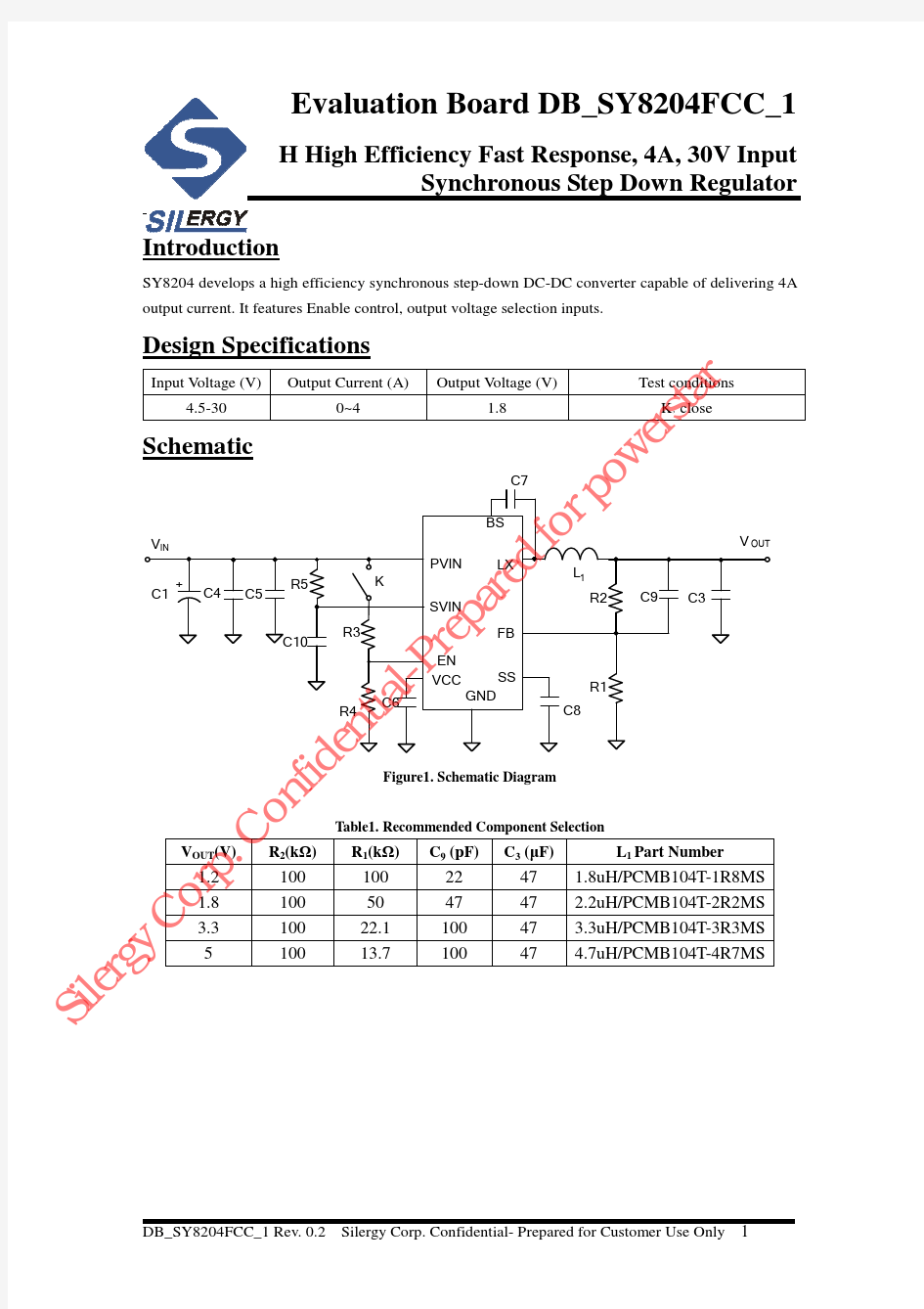
SY8204 develops a high efficiency synchronous step-down DC-DC converter capable of delivering 4A output current. It features Enable control, output voltage selection inputs.
Design Specifications
4.5-30 0~4 1.8
C7 BS VIN PVIN C1
+
fo
rp
ow
V OUT L1 R2 C9 C3 R1 C8
Schematic
C4
C5
R5 R3
K
tia l-P re p
SVIN
C10
EN VCC
R4
C6
fid
en
Figure1. Schematic Diagram
.C on
Table1. Recommended Component Selection
VOUT(V)
R2(k?)
R1(k?)
C9 (pF)
ar ed
LX
FB SS
GND
C3 (μF)
L1 Part Number
Co rp
Sil
er gy
1.2 1.8 3.3 5
100 100 100 100
100 50 22.1 13.7
22 47 100 100
47 47 47 47
1.8uH/PCMB104T-1R8MS 2.2uH/PCMB104T-2R2MS 3.3uH/PCMB104T-3R3MS 4.7uH/PCMB104T-4R7MS
DB_SY8204FCC_1 Rev. 0.2
Silergy Corp. Confidential- Prepared for Customer Use Only 1
er sta
Input Voltage (V)
Output Current (A)
Output Voltage (V)
Test conditions K,close
r
Evaluation Board DB_SY8204FCC_1
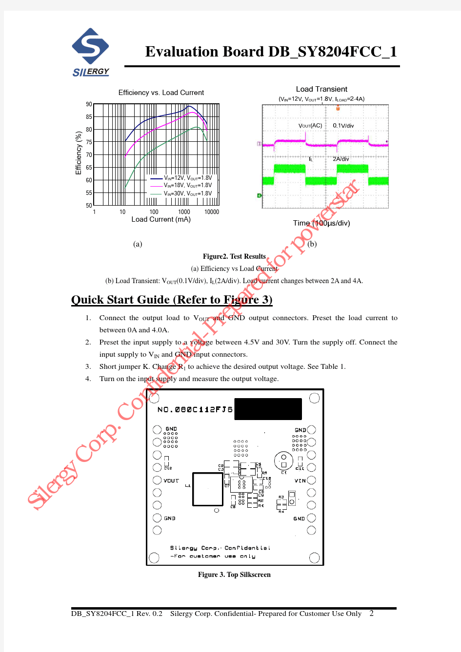
Efficiency vs. Load Current
90 85 80 75 70 65 60 55 50 1 10 100 1000 10000 VIN=12V, VOUT=1.8V VIN=18V, VOUT=1.8V VIN=30V, VOUT=1.8V
Load Current (mA)
Figure2. Test Results
(a) Efficiency vs Load Current
1. 2. 3. 4.
Connect the output load to VOUT and GND output connectors. Preset the load current to between 0A and 4.0A. Preset the input supply to a voltage between 4.5V and 30V. Turn the supply off. Connect the input supply to VIN and GND input connectors. Short jumper K. Change R1 to achieve the desired output voltage. See Table 1.
Sil
er gy
Co rp
.C on
fid
Turn on the input supply and measure the output voltage.
en
DB_SY8204FCC_1 Rev. 0.2
tia l-P re p
Quick Start Guide (Refer to Figure 3)
Figure 3. Top Silkscreen
Silergy Corp. Confidential- Prepared for Customer Use Only 2
ar ed
(b) Load Transient: VOUT(0.1V/div), IL(2A/div). Load current changes between 2A and 4A.
fo
rp
(a)
ow
(b)
er sta
r
Evaluation Board DB_SY8204FCC_1
PCB Layout
(a)
rp tia l-P re p
Description
BOM List
Designator
ar ed
Figure 4. PCB Layout Plots: (a) top layer, (b) bottom layer
fo
Part Number Manufacturer
C1 C3 C4
、C5
47uF/50V Electrolytic Cap 47uF/6.3V/X5R,1206 2.2uF/50V/X5R, 1206 1uF/16V/X7R, 0603
C3216X5R0J476M C3216X5R1H225K C1608X7R105K C1608X7R1H104K C1608X7R1H473K C1608C0G1H470J PCMB104T-2R2MS
ow
(b) TDK TDK TDK TDK TDK TDK CYNTEC C7 C8 C9 L1 R1 R2 R4
.C on
fid
C6
Co rp
er gy
R3
Sil
DB_SY8204FCC_1 Rev. 0.2
en
0.1uF/50V/X7R, 0603 47nF/50V/X7R, 0603 47pF/50V/C0G, 0603 2.2uH/12A 49.9k , 1%, 0603 100k , 1%, 0603 1M? , 1%, 0603 10k , 1%, 0603
Silergy Corp. Confidential- Prepared for Customer Use Only 3
er sta
r
Evaluation Board DB_SY8204FCC_1
Output Voltage Ripple Test
A proper output ripple measurement should be done according to Figure 5 setup. Output voltage ripple should be measured across the output ceramic cap near the IC. 1. Remove the ground clip and head of the probe. Wind thin wires around the ground ring of the probe. Solder the end of the ground ring wire to the negative node of the C3. Touch the probe tip to the positive node of the C3. Refer to Figure.5. 2. Minimize the loop formed by C3 terminals, probe tip and ground ring. 3. Change the probing direction to decouple the electromagnetic noise generated from the nearby buck
Figure.5 Recommended way to measure the output voltage ripple
Sil
er gy
Co rp
.C on
fid
DB_SY8204FCC_1 Rev. 0.2
en
tia l-P re p
Silergy Corp. Confidential- Prepared for Customer Use Only 4
ar ed
fo
rp
ow
er sta
inductor (Refer to Figure.5).
r