Computer-Aided Design for Emerging Technologies
- 格式:pdf
- 大小:960.19 KB
- 文档页数:10

IEEE Transactions, Journals, and LettersAdvanced Packaging, IEEE Transactions onAerospace and Electronic Syst ems, IEEE Transactions onAntennas and Propagation, IEEE Transactions onAntennas and Wireless Propagation LettersApplied Superconductivit y, IEEE Transactions onAudio, Speech and Language Processing, IEEE Transactions onAutomatic Cont rol, IEEE Transactions onAutomation Science and Engineering, IEEE Transactions onBiomedical Circuits and Systems, IEEE Transactions onBiomedical Engineering, IEEE Transactions onBroadcasting, IEEE Transactions onCircuits and Systems for Video Technology, IEEE Transactions onCircuits and Systems I: Regular Papers, IEEE Transactions onCircuits and Systems II: Express Briefs, IEEE Transactions onCommunications Letters, IEEECommunications Magazine, IEEECommunications, IEEE Transactions onComponents and Packaging Technologies, IEEE Transactions onComput ational Biology and Bioinformatics, IEEE/ACM Transactions onComput er Archit ecture Lett ers, IEEEComput er-Aided Design of Int egrat ed Circuits and Systems, IEEE Transactions on Comput ers, IEEE Transactions onComputing in Science & EngineeringConsumer Elect ronics, IEEE Transactions onCont rol Syst ems Technology, IEEE Transactions onDependable and Secure Computing, IEEE Transactions onDevice and Materials Reliabilit y, IEEE Transactions onDielectrics and Electrical Insulation, IEEE Transactions onDisplay Technology, Journal ofEducation, IEEE Transactions onElect rical and Computer Engineering, Canadian Journal ofElect romagnetic Compatibilit y, IEEE Transactions onElect ron Device Letters, IEEEElect ron Devices, IEEE Transactions onElect ronic Materials, IEEE/TMS Journal ofElect ronics Packaging Manufacturing, IEEE Transactions onEnergy Conversion, IEEE Transactions onEngineering Management, IEEE Transactions onGeoscience and Remote Sensing Letters, IEEEGeoscience and Remote Sensing, IEEE Transactions onImage Processing, IEEE Transactions onIndustrial Elect ronics, IEEE Transactions onIndustrial Informatics, IEEE Transactions onIndustry Applications, IEEE Transactions onInformation Forensics and Securit y, IEEE Transactions on Information Technology in Biomedicine, IEEE Transactions on Information Theory, IEEE Transactions onInstrument ation and Measurement, IEEE Transactions onIntelligent Transport ation Syst ems, IEEE Transactions onKnowledge and Data Engineering, IEEE Transactions onLatin America Transactions, IEEELightwave Technology, Journal ofMagnetics, IEEE Transactions onManufacturing Technology, IEEE Transactions onMechatronics, IEEE/ASME Transactions onMedical Imaging, IEEE Transactions onMicroelect romechanical Syst ems, Journal ofMicrowave and Wireless Components Letters, IEEEMicrowave Theory and Techniques, IEEE Transactions onMobile Computing, IEEE Transactions onMultimedia, IEEE Transactions onNanobioscience, IEEE Transactions onNanot echnology, IEEE Transactions onNetwork and Service Management, IEEE Transactions on Networking, IEEE/ACM Transactions onNeural Networks, IEEE Transactions onNeural Syst ems and Rehabilitation Engineering, IEEE Transactions on Nuclear Science, IEEE Transactions onOceanic Engineering, IEEE Journal ofParallel and Distributed Systems, IEEE Transactions onPattern Analysis and Machine Intelligence, IEEE Transactions onPhot onics Journals, IEEEPhot onics Technology Letters, IEEEPlasma Science, IEEE Transactions onPower Delivery, IEEE Transactions onPower Electronics Letters, IEEEPower Electronics, IEEE Transactions onPower Systems, IEEE Transactions onProfessional Communication, IEEE Transactions onProject Safet y Engineering, IEEE Journal onQuantum Electronics, IEEE Journal ofReliability, IEEE Transactions onRobotics, IEEE Transactions onSelected Areas in Communications, IEEE Journal onSelected Topics in Signal Processing, IEEE Journal onSelected Topics in Quantum Electronics, IEEE Journal ofSemiconduct or Manufacturing, IEEE Transactions onSensors Journal, IEEESignal Processing Lett ers, IEEESignal Processing, IEEE Transactions onSoft ware Engineering, IEEE Transactions onSolid-State Circuit s, IEEE Journal ofSystems Journal, IEEESystems, Man and Cybernetics, Part A, IEEE Transactions onSystems, Man and Cybernetics, Part B, IEEE Transactions onSystems, Man and Cybernetics, Part C, IEEE Transactions onUltrasonics, Ferroelect rics and F requency Cont rol, IEEE Transactions onVehicular Technology, IEEE Transactions onVery Large Scale Integration (VLSI) Systems, IEEE Transactions onVisualization and Computer Graphics, IEEE Transactions onWireless Communications, IEEE Transactions ontop of pageIEEE MagazinesAerospace & Electronics Systems Magazine, IEEEAnnals of the History of Computing, IEEEAntennas & Propagation Magazine, IEEECircuits & Devices Magazine, IEEECircuits and Systems Magazine, IEEECommunications, IEEECommunications Surveys and Tut orials, IEEEComput erComput er Graphics & Applications, IEEEComput ational Intelligence magazine IEEECont rol Syst ems Magazine, IEEEDesign & Test of Comput ers, IEEEEngineering in Medicine & Biology Magazine, IEEEInstrument ation & Measurement Magazine, IEEEIntelligent Systems, IEEEIntelligent Transport ation Syst ems, IEEEInternet Computing, IEEEIT ProfessionalMicro, IEEEMicrowave Magazine, IEEE MultiMedia, IEEENetwork, IEEEPervasive Computing, IEEEPot entials, IEEESecurity and Privacy Magazine, IEEE Signal Processing Magazine, IEEE Soft ware, IEEESolid-State Circuit s, IEEE Spectrum, IEEETechnology & Societ y Magazine, IEEE Vehicular Technology Magazine IEEE Wireless Communications, IEEE。
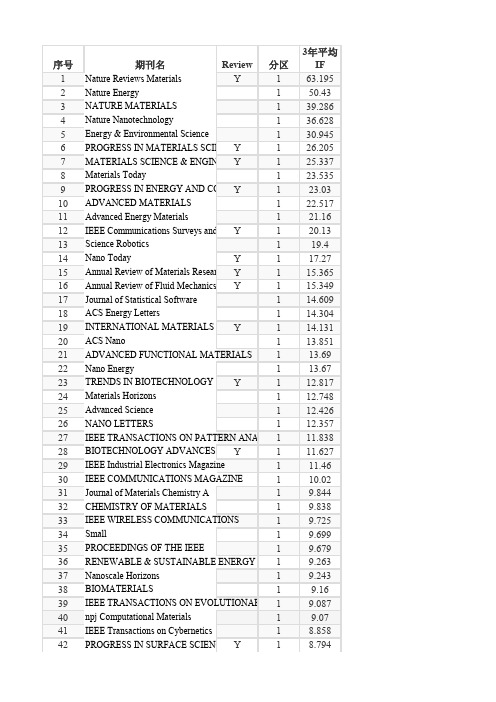
序号期刊名Review分区3年平均IF1Nature Reviews Materials Y163.195 2Nature Energy150.43 3NATURE MATERIALS139.286 4Nature Nanotechnology136.628 5Energy & Environmental Science130.945 6PROGRESS IN MATERIALS SCIEN Y126.205 7MATERIALS SCIENCE & ENGINEE Y125.337 8Materials Today123.535 9PROGRESS IN ENERGY AND COM Y123.03 10ADVANCED MATERIALS122.517 11Advanced Energy Materials121.16 12IEEE Communications Surveys and T Y120.13 13Science Robotics119.4 14Nano Today Y117.27 15Annual Review of Materials Research Y115.365 16Annual Review of Fluid Mechanics Y115.349 17Journal of Statistical Software114.609 18ACS Energy Letters114.304 19INTERNATIONAL MATERIALS RE Y114.131 20ACS Nano113.851 21ADVANCED FUNCTIONAL MATERIALS113.69 22Nano Energy113.67 23TRENDS IN BIOTECHNOLOGY Y112.817 24Materials Horizons112.748 25Advanced Science112.426 26NANO LETTERS112.357 27IEEE TRANSACTIONS ON PATTERN ANALY111.838 28BIOTECHNOLOGY ADVANCES Y111.627 29IEEE Industrial Electronics Magazine111.46 30IEEE COMMUNICATIONS MAGAZINE110.02 31Journal of Materials Chemistry A19.844 32CHEMISTRY OF MATERIALS19.838 33IEEE WIRELESS COMMUNICATIONS19.725 34Small19.699 35PROCEEDINGS OF THE IEEE19.679 36RENEWABLE & SUSTAINABLE ENERGY RE19.263 37Nanoscale Horizons19.243 38BIOMATERIALS19.16 39IEEE TRANSACTIONS ON EVOLUTIONARY19.087 40npj Computational Materials19.07 41IEEE Transactions on Cybernetics18.858 42PROGRESS IN SURFACE SCIENCE Y18.79443INTERNATIONAL JOURNAL OF COMPUTER18.611 44IEEE Transactions on Neural Networks and Learn18.591 45CURRENT OPINION IN BIOTECHN Y18.586 46BIOSENSORS & BIOELECTRONICS18.49 47Annual Review of Food Science and T Y18.448 48IEEE TRANSACTIONS ON FUZZY SYSTEMS18.282 49IEEE SIGNAL PROCESSING MAGAZINE18.236 50IEEE JOURNAL ON SELECTED AREAS IN CO18.186 51IEEE Transactions on Smart Grid18.165 52NPG Asia Materials18.139 53ACS Applied Materials & Interfaces18.019 54Applied Materials Today18.013 55Nano Research17.954 56METABOLIC ENGINEERING17.875 57APPLIED ENERGY17.836 58Information Fusion17.674 59IEEE Internet of Things Journal17.662 60Annual Review of Chemical and Biom Y17.605 61IEEE NETWORK17.31 62Applied Mechanics Reviews Y17.302 63CURRENT OPINION IN SOLID STA Y17.301 64COMPREHENSIVE REVIEWS IN FO Y17.247 65IEEE TRANSACTIONS ON INDUSTRIAL ELE17.24 66Nanoscale17.19 67Additive Manufacturing17.173 68Advanced Optical Materials17.143 69JOURNAL OF CATALYSIS17.109 702D Materials17.107 71CHEMICAL ENGINEERING JOURNAL17.102 72Nano-Micro Letters17.091 73IEEE TRANSACTIONS ON POWER ELECTRO17.062 74PROGRESS IN PHOTOVOLTAICS1 6.986 75REMOTE SENSING OF ENVIRONMENT1 6.98 76CARBON1 6.962 77IEEE Transactions on Cloud Computing1 6.948 78JOURNAL OF POWER SOURCES1 6.936 79ACS Photonics1 6.926 80Virtual and Physical Prototyping1 6.825 81INTERNATIONAL JOURNAL OF ENGINEERI1 6.779 82TRENDS IN FOOD SCIENCE & TEC Y1 6.773 83Soft Robotics1 6.703 84Polymer Reviews Y1 6.638 85JOURNAL OF MEMBRANE SCIENCE1 6.543 86IEEE Transactions on Industrial Informatics1 6.52487Acta Biomaterialia1 6.447 88ISPRS JOURNAL OF PHOTOGRAMMETRY A1 6.441 89Biofabrication1 6.438 90ENERGY CONVERSION AND MANAGEMEN1 6.382 91CRITICAL REVIEWS IN FOOD SCI Y1 6.328 92LAB ON A CHIP1 6.318 93ARCHIVES OF COMPUTATIONAL Y1 6.303 94CRITICAL REVIEWS IN BIOTECHN Y1 6.278 95IEEE Computational Intelligence Magazine1 6.27 96IEEE Transactions on Sustainable Energy1 6.265 97Advances in Applied Mechanics Y1 6.222 98ACTA MATERIALIA1 6.21 99Materials Research Letters1 6.125 100NEURAL NETWORKS1 6.09 101DESALINATION1 6.055 102BIORESOURCE TECHNOLOGY1 6.042 103AUTOMATICA1 5.977 104Journal of Materials Chemistry C1 5.958 105IEEE TRANSACTIONS ON POWER SYSTEMS1 5.914 106COMPUTER-AIDED CIVIL AND INFRASTRU1 5.823 107SENSORS AND ACTUATORS B-CHEMICAL1 5.82 108Nanophotonics1 5.805 109IEEE TRANSACTIONS ON WIRELESS COMM1 5.744 110INTERNATIONAL JOURNAL OF PLASTICITY1 5.668 111Advanced Healthcare Materials1 5.663 112IEEE TRANSACTIONS ON IMAGE PROCESSI1 5.563 113IEEE Vehicular Technology Magazine1 5.537 114COMPOSITES PART B-ENGINEERING1 5.504 115IEEE CONTROL SYSTEMS MAGAZINE1 5.495 116CORROSION SCIENCE1 5.487 117IEEE Transactions on Information Forensics and 1 5.456 118IEEE Journal of Selected Topics in Signal Proces1 5.45 119COMPOSITES SCIENCE AND TECHNOLOGY1 5.447 120Microsystems & Nanoengineering1 5.344 121Science China-Materials1 4.637 122Journal of Magnesium and Alloys1 4.523 123JOURNAL OF MATERIALS SCIENCE & TECH1 3.804 124CHINESE JOURNAL OF CATALYSIS1 3.751 125Engineering1 3.617 126Petroleum Exploration and Development1 2.169 127CRITICAL REVIEWS IN SOLID STA Y2 6.189 128ACM COMPUTING SURVEYS Y2 6.143 129Biotechnology for Biofuels2 5.384 130CARBOHYDRATE POLYMERS2 5.338131Advanced Electronic Materials2 5.324 132SOLAR ENERGY MATERIALS AND SOLAR C2 5.274 133CEMENT AND CONCRETE RESEARCH2 5.27 134IEEE Transactions on Transportation Electrificati2 5.27 135FOOD HYDROCOLLOIDS2 5.225 136JOURNAL OF NANOBIOTECHNOLOGY2 5.195 137INTERNATIONAL JOURNAL OF ROBOTICS 2 5.161 138PROGRESS IN AEROSPACE SCIEN Y2 5.154 139IEEE Journal of Emerging and Selected Topics in2 5.139 140Frontiers in Bioengineering and Biotechnology2 5.122 141ELECTROCHIMICA ACTA2 5.099 142Biomaterials Science2 5.097 143IEEE TRANSACTIONS ON GEOSCIENCE AN2 5.078 144INTERNATIONAL JOURNAL OF MACHINE T2 5.047 145ENERGY2 5.008 146Advanced Materials Technologies2 5.008 147SEPARATION AND PURIFICATION Y2 5.001 148Journal of CO2 Utilization2 4.995 149ACM TRANSACTIONS ON GRAPHICS2 4.989 150Global Change Biology Bioenergy2 4.973 151FOOD CHEMISTRY2 4.958 152COMPOSITES PART A-APPLIED SCIENCE AN2 4.957 153IEEE Transactions on Systems Man Cybernetics-2 4.945 154IEEE Transactions on Robotics2 4.928 155Sustainable Energy & Fuels2 4.912 156RENEWABLE ENERGY2 4.899 157MRS BULLETIN2 4.889 158INFORMATION SCIENCES2 4.887 159MATERIALS & DESIGN2 4.886 160FUEL2 4.879 161PATTERN RECOGNITION2 4.815 162IEEE TRANSACTIONS ON COMMUNICATIO2 4.806 163IEEE Transactions on Control of Network System2 4.802 164Future Generation Computer Systems-The Interna2 4.801 165IEEE TRANSACTIONS ON AUTOMATIC CON2 4.79 166Journal of Materials Chemistry B2 4.789 167INTERNATIONAL JOURNAL OF COAL GEOL2 4.748 168JOURNAL OF INDUSTRIAL AND ENGINEER2 4.747 169Materials Science & Engineering C-Materials for2 4.734 170IEEE TRANSACTIONS ON CONTROL SYSTE2 4.712 171MOLECULAR NUTRITION & FOOD RESEAR2 4.709 172CEMENT & CONCRETE COMPOSITES2 4.699 173Swarm and Evolutionary Computation2 4.68 174KNOWLEDGE-BASED SYSTEMS2 4.675175IEEE Transactions on Affective Computing2 4.674 176COMPUTERS & EDUCATION2 4.661 177IEEE TRANSACTIONS ON VEHICULAR TEC2 4.612 178INTEGRATED COMPUTER-AIDED ENGINEE2 4.612 179Advanced Materials Interfaces2 4.609 180IEEE Transactions on Dependable and Secure Co2 4.58 181IEEE TRANSACTIONS ON SIGNAL PROCESS2 4.578 182IEEE Transactions on Services Computing2 4.548 183IEEE Transactions on Computational Imaging2 4.546 184TRANSPORTATION RESEARCH PART C-EM2 4.516 185INTERNATIONAL JOURNAL OF INTELLIGE2 4.507 186IEEE TRANSACTIONS ON INTELLIGENT TR2 4.506 187MECHANICAL SYSTEMS AND SIGNAL PRO2 4.497 188IEEE JOURNAL OF SOLID-STATE CIRCUITS2 4.476 189BUILDING AND ENVIRONMENT2 4.471 190ELECTROCHEMISTRY COMMUNICATIONS2 4.418 191Nonlinear Analysis-Hybrid Systems2 4.413 192IEEE-ASME TRANSACTIONS ON MECHATR2 4.412 193COMPUTER METHODS IN APPLIED MECHA2 4.404 194SOLAR ENERGY2 4.355 195PARTICLE & PARTICLE SYSTEMS CHARAC2 4.351 196ENERGY AND BUILDINGS2 4.34 197APPLIED SURFACE SCIENCE2 4.327 198IEEE TRANSACTIONS ON MULTIMEDIA2 4.313 199INTERNATIONAL JOURNAL OF PRODUCTIO2 4.299 200COMPOSITE STRUCTURES2 4.263 201JOURNAL OF NETWORK AND COMPUTER A2 4.255 202APL Materials2 4.253 203BIOTECHNOLOGY AND BIOENGINEERING2 4.231 204Journal of Field Robotics2 4.229 205IEEE Systems Journal2 4.227 206COMMUNICATIONS OF THE ACM2 4.167 207Foundations and Trends in Informatio Y2 4.161 208SCRIPTA MATERIALIA2 4.15 209IEEE Transactions on Emerging Topics in Compu2 4.147 210TRANSPORTATION RESEARCH PART B-ME2 4.141 211NONLINEAR DYNAMICS2 4.136 212JOURNAL OF PHYSICAL AND CHEMICAL R2 4.133 213IEEE TRANSACTIONS ON MOBILE COMPUT2 4.131 214IEEE Transactions on Automation Science and En2 4.131 215SEPARATION AND PURIFICATION TECHNO2 4.131 216APPLIED SOFT COMPUTING2 4.107 217ARTIFICIAL INTELLIGENCE2 4.105 218INTERNATIONAL COMMUNICATIONS IN H2 4.103219COMBUSTION AND FLAME2 4.092 220STRUCTURAL HEALTH MONITORING-AN I2 4.091 221Extreme Mechanics Letters2 4.075 222FUEL PROCESSING TECHNOLOGY2 4.072 223IEEE TRANSACTIONS ON ENERGY CONVER2 4.063 224ACS Biomaterials Science & Engineering2 4.059 225SCIENCE AND TECHNOLOGY OF ADVANCE2 4.057 226IEEE TRANSACTIONS ON BROADCASTING2 4.016 227IEEE JOURNAL OF SELECTED TOPICS IN QU2 4.006 228EXPERT SYSTEMS WITH APPLICATIONS2 3.996 229FOOD MICROBIOLOGY2 3.979 230Vehicular Communications2 3.976 231Microbial Cell Factories2 3.971 232JOURNAL OF THE MECHANICS AND PHYSI2 3.969 233Journal of the Taiwan Institute of Chemical Engin2 3.967 234Current Opinion in Chemical Engineer Y2 3.966 235INTERNATIONAL JOURNAL OF HYDROGEN2 3.965 236REVIEWS IN CHEMICAL ENGINEE Y2 3.954 237Journal of Biophotonics2 3.953 238COLLOIDS AND SURFACES B-BIOINTERFAC2 3.952 239PROCEEDINGS OF THE COMBUSTION INST2 3.95 240GPS SOLUTIONS2 3.946 241International Journal of Precision Engineering an2 3.943 242INTERNATIONAL JOURNAL OF HEAT AND 2 3.898 243IEEE TRANSACTIONS ON PARALLEL AND D2 3.851 244ARTIFICIAL INTELLIGENCE REVIEW2 3.845 245IEEE TRANSACTIONS ON ANTENNAS AND 2 3.841 246IEEE Journal of Biomedical and Health Informati2 3.839 247Energy Reports2 3.83 248JOURNAL OF LIGHTWAVE TECHNOLOGY2 3.828 249MICROPOROUS AND MESOPOROUS MATER2 3.815 250FOOD CONTROL2 3.804 251HUMAN-COMPUTER INTERACTION2 3.802 252NEURAL COMPUTING & APPLICATIONS2 3.795 253IEEE TRANSACTIONS ON SOFTWARE ENGI2 3.794 254JOURNAL OF MACHINE LEARNING RESEAR2 3.791 255Current Opinion in Food Science Y2 3.781 256INTERNATIONAL JOURNAL OF ELECTRICA2 3.772 257Biofuels Bioproducts & Biorefining-Biofpr2 3.765 258New Biotechnology2 3.762 259JOURNAL OF THE EUROPEAN CERAMIC SO2 3.759 260AUTOMATION IN CONSTRUCTION2 3.755 261DYES AND PIGMENTS2 3.753 262APPLIED THERMAL ENGINEERING2 3.747263Cognitive Computation2 3.736 264IEEE TRANSACTIONS ON CIRCUITS AND SY2 3.734 265INTERNATIONAL JOURNAL OF ROBUST AN2 3.734 266JOURNAL OF THE ENERGY INSTITUTE2 3.732 267CELLULOSE2 3.714 268ISA TRANSACTIONS2 3.702 269IEEE Transactions on Network and Service Mana2 3.701 270IEEE ROBOTICS & AUTOMATION MAGAZIN2 3.7 271Nanomaterials2 3.697 272Alexandria Engineering Journal2 3.696 273JOURNAL OF ALLOYS AND COMPOUNDS2 3.696 274International Journal of Greenhouse Gas Control2 3.683 275IEEE TRANSACTIONS ON POWER DELIVER2 3.661 276JOURNAL OF MATERIALS PROCESSING TE2 3.657 277IEEE Cloud Computing2 3.652 278IEEE Access2 3.633 279Internet Research2 3.626 280IEEE TRANSACTIONS ON NEURAL SYSTEM2 3.62 281INTERNATIONAL JOURNAL OF FOOD MICR2 3.599 282Remote Sensing2 3.589 283JOURNAL OF SANDWICH STRUCTURES & M2 3.575 284ROBOTICS AND COMPUTER-INTEGRATED 2 3.567 285CONSTRUCTION AND BUILDING MATERIA2 3.567 286STEEL AND COMPOSITE STRUCTURES2 3.564 287SIGNAL PROCESSING2 3.555 288EMPIRICAL SOFTWARE ENGINEERING2 3.555 289DECISION SUPPORT SYSTEMS2 3.545 290APPLIED CLAY SCIENCE2 3.544 291NEUROCOMPUTING2 3.543 292MATERIALS SCIENCE AND ENGINEERING A2 3.53 293INTERNATIONAL JOURNAL OF MECHANIC2 3.529 294ORGANIC ELECTRONICS2 3.525 295Journal of Energy Storage2 3.517 296FOOD QUALITY AND PREFERENCE2 3.512 297High Voltage2 3.508 298TRANSPORTATION RESEARCH PART E-LOG2 3.505 299IEEE Circuits and Systems Magazine2 3.495 300Food Packaging and Shelf Life2 3.488 301INTERNATIONAL JOURNAL OF THERMAL S2 3.488 302APPLIED MICROBIOLOGY AND BIOTECHNO2 3.477 303ADVANCES IN ENGINEERING SOFTWARE2 3.464 304JOURNAL OF THE FRANKLIN INSTITUTE-E2 3.456 305Sustainable Energy Technologies and Assessmen2 3.456 306BUILDING RESEARCH AND INFORMATION2 3.449307COMPUTERS IN INDUSTRY2 3.437 308Journal of Tissue Engineering2 3.415 309NANOTECHNOLOGY2 3.414 310JOURNAL OF INTELLIGENT MANUFACTUR2 3.412 311IEEE ELECTRON DEVICE LETTERS2 3.411 312OPTICS AND LASERS IN ENGINEERING2 3.405 313IEEE Journal of Photovoltaics2 3.395 314FOOD RESEARCH INTERNATIONAL2 3.395 315BIOMASS & BIOENERGY2 3.371 316JOURNAL OF MANUFACTURING SYSTEMS2 3.37 317IEEE PERVASIVE COMPUTING2 3.362 318IEEE-ACM TRANSACTIONS ON NETWORKI2 3.361 319IEEE TRANSACTIONS ON KNOWLEDGE AN2 3.357 320CIRP ANNALS-MANUFACTURING TECHNO2 3.351 321STRUCTURAL SAFETY2 3.348 322JOURNAL OF THE ELECTROCHEMICAL SOC2 3.347 323FOOD POLICY2 3.328 324Nano Convergence2 3.324 325IEEE Intelligent Transportation Systems Magazin2 3.322 326TRANSPORTATION SCIENCE2 3.308 327JOURNAL OF FOOD ENGINEERING2 3.307 328INTERMETALLICS2 3.304 329TRANSPORTATION RESEARCH PART D-TR2 3.279 330Journal of the Mechanical Behavior of Biomedica2 3.278 331USER MODELING AND USER-ADAPTED INT2 3.278 332IEEE TRANSACTIONS ON MICROWAVE TH2 3.276 333ROCK MECHANICS AND ROCK ENGINEERI2 3.275 334Journal of Functional Foods2 3.27 335ADVANCED ENGINEERING INFORMATICS2 3.27 336Innovative Food Science & Emerging Technologi2 3.258 337COASTAL ENGINEERING2 3.248 338IET Renewable Power Generation2 3.243 339INFORMATION PROCESSING & MANAGEM2 3.242 340Structural Control & Health Monitoring2 3.239 341ANNUAL REVIEWS IN CONTROL Y2 3.235 342INTERNATIONAL JOURNAL OF FATIGUE2 3.235 343IEEE TRANSACTIONS ON VISUALIZATION 2 3.233 344Ad Hoc Networks2 3.229 345EVOLUTIONARY COMPUTATION2 3.228 346TRIBOLOGY INTERNATIONAL2 3.222 347AICHE JOURNAL2 3.208 348Nanoscale and Microscale Thermophysical Engin2 3.205 349JOURNAL OF SUPERCRITICAL FLUIDS2 3.198 350Business & Information Systems Engineering2 3.196351POWDER TECHNOLOGY2 3.195 352JOURNAL OF RHEOLOGY2 3.191 353CHEMICAL ENGINEERING SCIENCE2 3.191 354Sustainable Energy Grids & Networks2 3.182 355ChemNanoMat2 3.18 356JOURNAL OF BIOMEDICAL MATERIALS RE2 3.176 357EXPERIMENTAL THERMAL AND FLUID SC2 3.176 358MACROMOLECULAR BIOSCIENCE2 3.175 359Journal of Water Process Engineering2 3.173 360CERAMICS INTERNATIONAL2 3.164 361IEEE Antennas and Wireless Propagation Letters2 3.164 362BIOCHEMICAL ENGINEERING JOURNAL2 3.163 363Sustainable Cities and Society2 3.158 364Applied Nanoscience2 3.158 365COMPUTERS & CHEMICAL ENGINEERING2 3.157 366Polymers2 3.154 367IEEE Transactions on Signal and Information Pro2 3.153 368INTERNATIONAL JOURNAL OF IMPACT EN2 3.152 369IEEE Power & Energy Magazine2 3.147 370IEEE INTELLIGENT SYSTEMS2 3.145 371MEAT SCIENCE2 3.143 372Smart Materials and Structures2 3.138 373Journal of Natural Gas Science and Engineering2 3.127 374Materials Science and Engineering B-Advanced F2 3.125 375HYDROMETALLURGY2 3.123 376INDUSTRIAL & ENGINEERING CHEMISTRY2 3.12 377IET Control Theory and Applications2 3.119 378COMPUTERS & INDUSTRIAL ENGINEERING2 3.112 379Journal of Astronomical Telescopes Instruments a2 3.11 380TRANSPORTATION RESEARCH PART A-POL2 3.109 381Ain Shams Engineering Journal2 3.091 382TRANSPORTATION2 3.08 383ENGINEERING APPLICATIONS OF ARTIFICI2 3.08 384JOURNAL OF BIOMEDICAL MATERIALS RE2 3.079 385PROGRESS IN ORGANIC COATINGS2 3.078 386REACTIVE & FUNCTIONAL POLYMERS2 3.067 387THIN-WALLED STRUCTURES2 3.066 388IEEE Journal on Emerging and Selected Topics in2 3.064 389INTERNATIONAL JOURNAL OF REFRIGERA2 3.063 390IEEE Geoscience and Remote Sensing Letters2 3.063 391STRUCTURAL AND MULTIDISCIPLINARY O2 3.059 392LWT-FOOD SCIENCE AND TECHNOLOGY2 3.057 393IEEE TRANSACTIONS ON CIRCUITS AND SY2 3.055 394ENERGY & FUELS2 3.045395METROLOGIA2 3.044 396Energy Technology2 3.042 397Nanoscale Research Letters2 3.039 398IEEE TRANSACTIONS ON COMPUTERS2 3.033 399IEEE Wireless Communications Letters2 3.03 400COMPUTERS & STRUCTURES2 3.029 401Journal of Materials Research and Technology-JM2 3.028 402IEEE Journal of Selected Topics in Applied Earth2 3.027 403COMPLEXITY2 3.014 404JOURNAL OF MATERIALS SCIENCE2 3.011 405EPJ Data Science2 3.01 406ACM Transactions on Intelligent Systems and Te2 3.01 407IEEE TRANSACTIONS ON INDUSTRY APPLI2 3.009 408Particuology2 2.674 409Progress in Natural Science-Materials Internation2 2.64 410Journal of Bionic Engineering2 2.392 411Frontiers of Chemical Science and Engineering2 2.388 412Science China-Information Sciences2 2.182 413Journal of Modern Power Systems and Clean Ene2 2.167 414Friction2 2.126 415Science China-Technological Sciences2 1.946 416TRANSACTIONS OF NONFERROUS METALS2 1.825 417Engineering Applications of Computational Fluid2 1.749 418Journal of Advanced Ceramics2 1.701 419Building Simulation2 1.694 420Chinese Journal of Aeronautics2 1.672 421Petroleum Science2 1.598 422RARE METALS2 1.491 423Acta Metallurgica Sinica-English Letters2 1.487 424APPLIED MATHEMATICS AND MECHANICS2 1.481 425CHINA OCEAN ENGINEERING20.663 426Regenerative Biomaterials3 3.382 427FOOD REVIEWS INTERNATIONAL Y3 3.011 428ENZYME AND MICROBIAL TECHNOLOGY3 2.996 429IEEE-ACM Transactions on Audio Speech and L3 2.991 4303D Printing and Additive Manufacturing3 2.984 431INTERNATIONAL JOURNAL OF ENERGY RE3 2.983 432IEEE MICROWAVE MAGAZINE3 2.98 433GEOTECHNIQUE3 2.979 434VLDB JOURNAL3 2.977 435IEEE Transactions on Terahertz Science and Tech3 2.975 436MECHANISM AND MACHINE THEORY3 2.969 437JOURNAL OF INDUSTRIAL MICROBIOLOGY3 2.969 438JOURNAL OF THE AMERICAN CERAMIC SO3 2.964439INDUSTRIAL MANAGEMENT & DATA SYST3 2.96 440INTERNATIONAL JOURNAL OF ROCK MEC3 2.958 441Big Data Research3 2.952 442Journal of Grid Computing3 2.951 443ADVANCED POWDER TECHNOLOGY3 2.951 444JOURNAL OF FLUID MECHANICS3 2.95 445COMPUTERS AND GEOTECHNICS3 2.947 446Acta Geotechnica3 2.942 447MATERIALS CHARACTERIZATION3 2.942 448Biomedical Materials3 2.935 449JOURNAL OF PROCESS CONTROL3 2.934 450Bioinspiration & Biomimetics3 2.932 451WIND ENERGY3 2.929 452Physical Review Materials3 2.926 453Energy for Sustainable Development3 2.918 454COMPUTATIONAL MECHANICS3 2.915 455COMPUTER COMMUNICATIONS3 2.906 456GEOTHERMICS3 2.905 457JOURNAL OF FOOD COMPOSITION AND AN3 2.901 458Wiley Interdisciplinary Reviews-Energ Y3 2.9 459SURFACE & COATINGS TECHNOLOGY3 2.896 460MIT Technology Review3 2.893 461JOURNAL OF MANUFACTURING SCIENCE A3 2.891 462MATERIALS RESEARCH BULLETIN3 2.891 463EUROPEAN JOURNAL OF MECHANICS A-SO3 2.886 464IET Power Electronics3 2.884 465Semantic Web3 2.879 466Energy Science & Engineering3 2.873 467IEEE SIGNAL PROCESSING LETTERS3 2.87 468Food and Bioprocess Technology3 2.869 469Journal of Manufacturing Processes3 2.864 470MACROMOLECULAR MATERIALS AND EN3 2.864 471AUTONOMOUS ROBOTS3 2.861 472ELECTRIC POWER SYSTEMS RESEARCH3 2.855 473COMPUTERS & OPERATIONS RESEARCH3 2.855 474COMPUTERS & SECURITY3 2.854 475IEEE ANTENNAS AND PROPAGATION MAG3 2.853 476TUNNELLING AND UNDERGROUND SPACE3 2.851 477ACM TRANSACTIONS ON MATHEMATICAL3 2.848 478DATA MINING AND KNOWLEDGE DISCOVE3 2.84 479JOURNAL OF GEOTECHNICAL AND GEOEN3 2.823 480CONTROL ENGINEERING PRACTICE3 2.817 481WEAR3 2.814 482NDT & E INTERNATIONAL3 2.814483COMPUTER-AIDED DESIGN3 2.813 484IEEE TRANSACTIONS ON ULTRASONICS FE3 2.812 485ULTRAMICROSCOPY3 2.805 486IEEE TRANSACTIONS ON RELIABILITY3 2.802 487CHEMICAL ENGINEERING RESEARCH & DE3 2.802 488IEEE Transactions on Human-Machine Systems3 2.796 489JOURNAL OF CHEMICAL TECHNOLOGY AN3 2.794 490Beilstein Journal of Nanotechnology3 2.788 491JOURNAL OF MAGNETISM AND MAGNETIC3 2.786 492JOURNAL OF SOUND AND VIBRATION3 2.778 493IEEE TRANSACTIONS ON INSTRUMENTATI3 2.772 494MINERALS ENGINEERING3 2.769 495MECHANICS OF MATERIALS3 2.769 496IEEE MULTIMEDIA3 2.768 497JOURNAL OF BIOTECHNOLOGY3 2.765 498MATERIALS AND MANUFACTURING PROC3 2.764 499INFORMATION SYSTEMS FRONTIERS3 2.764 500MATERIALS LETTERS3 2.759 501JOURNAL OF ENGINEERING EDUCATION3 2.756 502INFORMATION AND SOFTWARE TECHNOL3 2.747 503International Journal of Machine Learning and Cy3 2.745 504IEEE SENSORS JOURNAL3 2.735 505EARTHQUAKE ENGINEERING & STRUCTUR3 2.733 506Journal of Building Performance Simulation3 2.732 507Leukos3 2.731 508SENSORS3 2.728 509ACM TRANSACTIONS ON COMPUTER SYST3 2.727 510JOURNAL OF MECHANICAL DESIGN3 2.726 511IEEE COMMUNICATIONS LETTERS3 2.723 512MOBILE NETWORKS & APPLICATIONS3 2.715 513Molecular Systems Design & Engineering3 2.708 514INTERNATIONAL JOURNAL OF SOLIDS AN3 2.704 515ENGINEERING STRUCTURES3 2.699 516Journal of Optical Communications and Network3 2.699 517Materials3 2.698 518Frontiers in Neurorobotics3 2.697 519Pervasive and Mobile Computing3 2.697 520CHEMICAL ENGINEERING AND PROCESSIN3 2.697 521IEEE TRANSACTIONS ON INFORMATION TH3 2.694 522Computer Networks3 2.689 523IET Generation Transmission & Distribution3 2.687 524CSEE Journal of Power and Energy Systems3 2.68 525FOOD AND BIOPRODUCTS PROCESSING3 2.679 526IEEE SOFTWARE3 2.671527SOLID STATE IONICS3 2.664 528MRS Communications3 2.651 529JOURNAL OF POLYMER SCIENCE PART B-P3 2.644 530INTERNATIONAL JOURNAL OF MULTIPHA3 2.643 531IEEE TRANSACTIONS ON ELECTRON DEVI3 2.643 532BioEnergy Research3 2.642 533MECHATRONICS3 2.632 534SPE JOURNAL3 2.618 535JOURNAL OF COMPOSITES FOR CONSTRUC3 2.615 536IEEE Journal of the Electron Devices Society3 2.612 537SYNTHETIC METALS3 2.61 538Fuzzy Optimization and Decision Making3 2.61 539SYSTEMS & CONTROL LETTERS3 2.61 540Optical Materials Express3 2.61 541Archives of Civil and Mechanical Engineering3 2.608 542APPLIED MATHEMATICAL MODELLING3 2.603 543ADVANCED ENGINEERING MATERIALS3 2.6 544CHEMOMETRICS AND INTELLIGENT LABO3 2.597 545PLASMA CHEMISTRY AND PLASMA PROCE3 2.594 546Human-centric Computing and Information Scien3 2.59 547JOURNAL OF WIND ENGINEERING AND IND3 2.583 548THEORETICAL AND APPLIED FRACTURE M3 2.574 549INTERNATIONAL JOURNAL OF GENERAL S3 2.56 550International Journal of Fuzzy Systems3 2.56 551MATERIALS SCIENCE IN SEMICONDUCTOR3 2.558 552POLYMER TESTING3 2.551 553IEEE Photonics Journal3 2.549 554JOURNAL OF CHEMICAL THERMODYNAMI3 2.549 555Energies3 2.548 556ENGINEERING FRACTURE MECHANICS3 2.546 557Biomicrofluidics3 2.546 558IEEE TRANSACTIONS ON NANOTECHNOLO3 2.545 559SOFT COMPUTING3 2.541 560Progress in Electromagnetics Research-PIER3 2.533 561International Journal of Bio-Inspired Computation3 2.532 562IMAGE AND VISION COMPUTING3 2.521 563JOURNAL OF MANAGEMENT IN ENGINEER3 2.521 564Food Bioscience3 2.518 565INTERNATIONAL JOURNAL OF REFRACTO3 2.518 566SENSORS AND ACTUATORS A-PHYSICAL3 2.516 567RAPID PROTOTYPING JOURNAL3 2.516 568COMPUTER VISION AND IMAGE UNDERST3 2.511 569JOURNAL OF FLUIDS AND STRUCTURES3 2.508 570ROBOTICS AND AUTONOMOUS SYSTEMS3 2.505571PRECISION ENGINEERING-JOURNAL OF TH3 2.501 572INTERNATIONAL JOURNAL FOR NUMERIC3 2.499 573COMPUTATIONAL MATERIALS SCIENCE3 2.489 574Cellular and Molecular Bioengineering3 2.482 575NETWORKS & SPATIAL ECONOMICS3 2.48 576PLANT FOODS FOR HUMAN NUTRITION3 2.477 577Plasmonics3 2.477 578MATERIALS AND STRUCTURES3 2.475 579FATIGUE & FRACTURE OF ENGINEERING M3 2.474 580MARINE STRUCTURES3 2.469 581Food Security3 2.465 582INFORMATION SYSTEMS3 2.465 583Transportmetrica B-Transport Dynamics3 2.462 584IEEE PHOTONICS TECHNOLOGY LETTERS3 2.458 585DIGITAL SIGNAL PROCESSING3 2.457 586MEASUREMENT3 2.456 587MULTIBODY SYSTEM DYNAMICS3 2.456 588IEEE TRANSACTIONS ON CIRCUITS AND SY3 2.453 589SIAM Journal on Imaging Sciences3 2.453 590Advances in Biochemical Engineering Y3 2.453 591JOURNAL OF SOLID STATE ELECTROCHEM3 2.452 592DESIGN STUDIES3 2.443 593ACM SIGCOMM Computer Communication Rev3 2.442 594BMC BIOTECHNOLOGY3 2.441 595INTERNATIONAL JOURNAL OF FRACTURE3 2.435 596INTERNATIONAL JOURNAL OF ADVANCED3 2.435 597MATHEMATICS AND MECHANICS OF SOLI3 2.43 598International Journal of Engine Research3 2.428 599JOURNAL OF SYSTEMS AND SOFTWARE3 2.427 600IEEE-ACM Transactions on Computational Biolo3 2.426 601COMPUTER3 2.42 602Journal of Manufacturing Technology Manageme3 2.418 603OPTICAL MATERIALS3 2.415 604JOURNAL OF MATERIALS SCIENCE-MATER3 2.413 605INTERNATIONAL JOURNAL OF CONTROL3 2.413 606SEMICONDUCTOR SCIENCE AND TECHNOL3 2.413 607Smart Structures and Systems3 2.412 608JOURNAL OF MICROELECTROMECHANICA3 2.407 609JOURNAL OF NON-CRYSTALLINE SOLIDS3 2.404 610JOURNAL OF CONSTRUCTIONAL STEEL RE3 2.396 611Journal of Asian Ceramic Societies3 2.395 612FLUID PHASE EQUILIBRIA3 2.395 613INTERNATIONAL JOURNAL OF HUMAN-CO3 2.39 614VEHICLE SYSTEM DYNAMICS3 2.389615Microfluidics and Nanofluidics3 2.388 616JOURNAL OF VIBRATION AND CONTROL3 2.388 617Transportation Geotechnics3 2.385 618ACM Transactions on Sensor Networks3 2.381 619JOURNAL OF PETROLEUM SCIENCE AND E3 2.38 620International Journal of Mechanics and Materials3 2.38 621ACM Transactions on Multimedia Computing Co3 2.38 622PHYSICS OF FLUIDS3 2.379 623Journal of Building Engineering3 2.378 624SIGNAL PROCESSING-IMAGE COMMUNICA3 2.377 625IET Electric Power Applications3 2.376 626AEROSPACE SCIENCE AND TECHNOLOGY3 2.371 627JOURNAL OF NON-NEWTONIAN FLUID ME3 2.366 628Nano Communication Networks3 2.363 629DIAMOND AND RELATED MATERIALS3 2.361 630MATERIALS CHEMISTRY AND PHYSICS3 2.358 631Biointerphases3 2.356 632EARTHQUAKE SPECTRA3 2.355 633JOURNAL OF INTELLIGENT MATERIAL SYS3 2.349 634Frontiers in Materials3 2.349 635JOURNAL OF NUCLEAR MATERIALS3 2.347 636INTERNATIONAL JOURNAL FOR NUMERIC3 2.347 637JOURNAL OF APPLIED MECHANICS-TRANS3 2.344 638JOURNAL OF PHYSICS AND CHEMISTRY O3 2.339 639ENERGY JOURNAL3 2.339 640INTERNATIONAL DAIRY JOURNAL3 2.334 641CIRP Journal of Manufacturing Science and Tech3 2.333 642IEEE SPECTRUM3 2.331 643Journal of Mechanisms and Robotics-Transaction3 2.327 644JOURNAL OF CEREAL SCIENCE3 2.326 645BIODEGRADATION3 2.321 646INTERNATIONAL JOURNAL OF SYSTEMS S3 2.313 647IEEE JOURNAL OF OCEANIC ENGINEERING3 2.31 648RESEARCH IN ENGINEERING DESIGN3 2.307 649Egyptian Informatics Journal3 2.306 650IEEE Transactions on Cognitive and Developmen3 2.305 651APPLIED ERGONOMICS3 2.304 652REQUIREMENTS ENGINEERING3 2.297 653FINITE ELEMENTS IN ANALYSIS AND DESI3 2.29 654International Journal of Social Robotics3 2.288 655JOURNAL OF APPLIED ELECTROCHEMISTR3 2.288 656IEEE TRANSACTIONS ON NANOBIOSCIENC3 2.285 657Coatings3 2.285 658Cognitive Neurodynamics3 2.283659Flexible Services and Manufacturing Journal3 2.282 660Swarm Intelligence3 2.281 661OCEAN ENGINEERING3 2.279 662IEEE TRANSACTIONS ON AEROSPACE AND3 2.278 663JOURNAL OF BIOMATERIALS APPLICATIO3 2.278 664JOURNAL OF CHEMICAL AND ENGINEERIN3 2.272 665Memetic Computing3 2.268 666INTERNATIONAL JOURNAL OF ADHESION 3 2.259 667JOURNAL OF TURBOMACHINERY-TRANSA3 2.259 668Surface Topography-Metrology and Properties3 2.257 669APPLIED INTELLIGENCE3 2.256 670PATTERN RECOGNITION LETTERS3 2.253 671COMPUTERS & FLUIDS3 2.252 672MECCANICA3 2.241 673Journal of Photonics for Energy3 2.24 674MECHANICS OF ADVANCED MATERIALS A3 2.238 675ACM TRANSACTIONS ON INFORMATION S3 2.235 676Geomechanics for Energy and the Environment3 2.231 677MICROSCOPY AND MICROANALYSIS3 2.229 678Energy Strategy Reviews3 2.229 679KOREAN JOURNAL OF CHEMICAL ENGINE3 2.227 680IEEE JOURNAL OF QUANTUM ELECTRONIC3 2.225 681JOURNAL OF CONSTRUCTION ENGINEERIN3 2.223 682EXPERIMENTAL MECHANICS3 2.222 683Advances in Nano Research3 2.221 684JOURNAL OF COMPUTING IN CIVIL ENGINE3 2.221 685KNOWLEDGE AND INFORMATION SYSTEM3 2.216 686Automated Software Engineering3 2.21 687JOURNAL OF ENERGY RESOURCES TECHN3 2.21 688IEEE Transactions on Haptics3 2.209 689NUMERICAL HEAT TRANSFER PART A-APP3 2.207 690JOURNAL OF POLYMERS AND THE ENVIRO3 2.204 691Bulletin of Earthquake Engineering3 2.203 692COLD REGIONS SCIENCE AND TECHNOLOG3 2.2 693CONTINUUM MECHANICS AND THERMOD3 2.199 694INTERNATIONAL JOURNAL OF APPROXIM3 2.198 695Wiley Interdisciplinary Reviews-Data Y3 2.197 696Electronic Materials Letters3 2.184 697INTERNATIONAL JOURNAL OF FOOD SCIEN3 2.184 698JOURNAL OF MATERIALS SCIENCE-MATER3 2.179 699POLYMER COMPOSITES3 2.178 700ACM TRANSACTIONS ON SOFTWARE ENGI3 2.178 701HOLZFORSCHUNG3 2.175 702MACHINE LEARNING3 2.171703INTERNATIONAL JOURNAL OF MINERAL P3 2.168 704DRYING TECHNOLOGY3 2.167 705International Journal of Concrete Structures and M3 2.167 706Journal of Intelligent Transportation Systems3 2.167 707REVIEWS ON ADVANCED MATERIALS SCIE3 2.167 708Micromachines3 2.16 709SIMULATION MODELLING PRACTICE AND3 2.157 710EXPERIMENTS IN FLUIDS3 2.157 711JOURNAL OF HYDRAULIC ENGINEERING3 2.156 712INTERNATIONAL JOURNAL OF NON-LINEA3 2.154 713JOURNAL OF STRUCTURAL ENGINEERING3 2.151 714International Journal of Pavement Engineering3 2.151 715IEEE Transactions on Learning Technologies3 2.15 716IEEE TRANSACTIONS ON COMPUTER-AIDE3 2.144 717IEEE MICROWAVE AND WIRELESS COMPO3 2.143 718Journal of Cloud Computing-Advances Systems a3 2.14 719IEEE MICRO3 2.139 720TRANSPORT IN POROUS MEDIA3 2.138 721WORLD JOURNAL OF MICROBIOLOGY & B3 2.137 722CANADIAN JOURNAL OF REMOTE SENSING3 2.13 723BIOPROCESS AND BIOSYSTEMS ENGINEER3 2.127 724FLOW TURBULENCE AND COMBUSTION3 2.118 725Food Additives and Contaminants Part A-Chemis3 2.115 726SCIENCE AND TECHNOLOGY OF WELDING3 2.115 727IEEE INTERNET COMPUTING3 2.114 728BIOTECHNOLOGY PROGRESS3 2.113 729JOURNAL OF HYDRAULIC RESEARCH3 2.106 730Journal of Nanomaterials3 2.104 731JOM3 2.103 732TRIBOLOGY LETTERS3 2.103 733INTERNATIONAL JOURNAL OF FOOD SCIEN3 2.101 734JOURNAL OF THERMAL STRESSES3 2.096 735JOURNAL OF BIOSCIENCE AND BIOENGINE3 2.096 736INTERNATIONAL JOURNAL OF INFORMAT3 2.094 737Transportmetrica A-Transport Science3 2.09 738ENGINEERING WITH COMPUTERS3 2.089 739JOURNAL OF VISUAL COMMUNICATION A3 2.086 740ACTA ASTRONAUTICA3 2.082 741POLYMERS FOR ADVANCED TECHNOLOGI3 2.069 742SOIL DYNAMICS AND EARTHQUAKE ENGI3 2.067 743EUROPEAN JOURNAL OF LIPID SCIENCE A3 2.066 744CALPHAD-COMPUTER COUPLING OF PHAS3 2.062 745Fuel Cells3 2.062 746Physical Mesomechanics3 2.058。

第44卷 第12期 包 装 工 程2023年6月 PACKAGING ENGINEERING 273收稿日期:2023–01–05基金项目:国家社科基金艺术学项目(21BG131)作者简介:濮子涵(1999—),女,硕士生,主攻视觉传达与信息设计。
濮子涵,杨滨(江南大学 设计学院,江苏 无锡 214122)摘要:目的 研究人工智能辅助技术介入包装设计流程的多元方式,分析人工智能技术应用现状,推导出更适应当下包装设计市场需求的技术应用策略。
方法 通过分析包装设计流程中人工智能技术实际应用案例,总结智能技术介入背景下包装设计的转变,探讨技术的创新及应用的层次。
结合设计实践进一步研究技术的应用策略,展望人工智能技术在包装设计中的应用前景。
结论 人工智能辅助技术可从用户数据分析、个性化设计延展、方案智能优化等多个应用层面优化包装设计,带来更大的生产效益。
合理应用人工智能技术有助于转变设计思维、拓展包装设计形式。
在包装设计中根据不同应用场景,使用智能技术辅助设计,可以提升设计效率,满足当前数字化经济时代发展的需求。
关键词:人工智能技术;包装设计;图案设计中图分类号:TB482 文献标识码:A 文章编号:1001-3563(2023)12-0273-09 DOI :10.19554/ki.1001-3563.2023.12.030Application of Artificial Intelligence AidedTechnology in Packaging DesignPU Zi-han , YANG Bin(School of Design, Jiangnan University, Jiangsu Wuxi 214122, China)ABSTRACT: The work aims to study the multiple ways of AI aided technology in the packaging design process, analyze the application status of AI technology, and deduce the technology application strategy that is more suitable for the de-mand of the current packaging design market. By analyzing the actual application cases of AI technology in the packaging design process, the transformation of packaging design under the background of intelligent technology intervention was summarized and the innovation and application level of technology were discussed. Combined with the design practice, the application strategy of the technology was further studied, and the application prospect of AI technology in packaging design was put forward. AI aided technology can optimize packaging design from multiple application levels, such as user data analysis, personalized design extension and scheme intelligent optimization, and bring greater production benefits. The rational application of AI technology is helpful to change design thinking and expand packaging design forms. In packaging design, using intelligent technology to assist design according to different application scenarios can improve design efficiency and meet the development demands of the current digital economy era. KEY WORDS: AI technology; packaging design; pattern design作为21世纪三大尖端技术之一的人工智能(Artificial Intelligence ,AI )技术,凭借其强大的数据处理能力与学习能力在众多生产领域中发挥着重要作用。
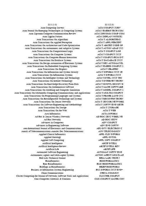
期刊全称期刊简称Acm Computing Surveys ACM COMPUT SURV Acm Journal On Emerging Technologies in Computing Systems ACM J EMERG TECH COM Acm Sigcomm Computer Communication Review ACM SIGCOMM COMP COMAcm Sigplan Notices ACM SIGPLAN NOTICES Acm Transactions On Algorithms ACM T ALGORITHMS Acm Transactions On Applied Perception ACM T APPL PERCEPT Acm Transactions On Architecture and Code Optimization ACM T ARCHIT CODE OPAcm Transactions On Autonomous and Adaptive Systems ACM T AUTON ADAP SYS Acm Transactions On Computational Logic ACM T COMPUT LOGAcm Transactions On Computer Systems ACM T COMPUT SYST Acm Transactions On Computer-Human Interaction ACM T COMPUT-HUM INT Acm Transactions On Database Systems ACM T DATABASE SYST Acm Transactions On Design Automation of Electronic Systems ACM T DES AUTOMAT EL Acm Transactions On Embedded Computing Systems ACM T EMBED COMPUT S Acm Transactions On Graphics ACM T GRAPHIC Acm Transactions On Information and System Security ACM T INFORM SYST SE Acm Transactions On Information Systems ACM T INFORM SYST Acm Transactions On Intelligent Systems and Technology ACM T INTEL SYST TEC Acm Transactions On Internet Technology ACM T INTERNET TECHN Acm Transactions On Knowledge Discovery From Data ACM T KNOWL DISCOV D Acm Transactions On Mathematical Software ACM T MATH SOFTWARE Acm Transactions On Modeling and Computer Simulation ACM T MODEL COMPUT S Acm Transactions On Multimedia Computing Communications and Applications ACM T MULTIM COMPUT Acm Transactions On Programming Languages and Systems ACM T PROGR LANG SYS Acm Transactions On Reconfigurable Technology and Systems ACM T RECONFIG TECHN Acm Transactions On Sensor Networks ACM T SENSOR NETWORK Acm Transactions On Software Engineering and Methodology ACM T SOFTW ENG METH Acm Transactions On Storage ACM T STORAGEAcm Transactions On the Web ACM T WEBActa Informatica ACTA INFORMAd Hoc & Sensor Wireless Networks AD HOC SENS WIREL NEAd Hoc Networks AD HOC NETWAdvances in Computers ADV COMPUTAdvances in Engineering Software ADV ENG SOFTW Aeu-International Journal of Electronics and Communications AEU-INT J ELECTRON C Annals of Telecommunications-Annales Des Telecommunications ANN TELECOMMUNApplied Clinical Informatics APPL CLIN INFORMApplied Ontology APPL ONTOLApplied Soft Computing APPL SOFT COMPUTArtificial Intelligence ARTIF INTELLArtificial Intelligence Review ARTIF INTELL REVArtificial Life ARTIF LIFEAutomated Software Engineering AUTOMAT SOFTW ENG Autonomous Agents and Multi-Agent Systems AUTON AGENT MULTI-AG Bell Labs Technical Journal BELL LABS TECH JBioinformatics BIOINFORMATICSBmc Bioinformatics BMC BIOINFORMATICSBriefings in Bioinformatics BRIEF BIOINFORM Business & Information Systems Engineering BUS INFORM SYST ENG+China Communications CHINA COMMUN Cluster Computing-the Journal of Networks Software Tools and Applications CLUSTER COMPUT Cmc-Computers Materials & Continua CMC-COMPUT MATER CONCmes-Computer Modeling in Engineering & Sciences CMES-COMP MODEL ENGCognitive Computation COGN COMPUTCognitive Systems Research COGN SYST RESCommunications of the Acm COMMUN ACMComputational Biology and Chemistry COMPUT BIOL CHEMComputational Geosciences COMPUTAT GEOSCIComputational Linguistics COMPUT LINGUISTComputer COMPUTERComputer Aided Geometric Design COMPUT AIDED GEOM D Computer Animation and Virtual Worlds COMPUT ANIMAT VIRT W Computer Applications in Engineering Education COMPUT APPL ENG EDUCComputer Communications COMPUT COMMUNComputer Graphics Forum COMPUT GRAPH FORUMComputer Journal COMPUT JComputer Languages Systems & Structures COMPUT LANG SYST STR Computer Methods and Programs in Biomedicine COMPUT METH PROG BIO Computer Methods in Applied Mechanics and Engineering COMPUT METHOD APPL M Computer Methods in Biomechanics and Biomedical Engineering COMPUT METHOD BIOMECComputer Music Journal COMPUT MUSIC JComputer Networks COMPUT NETW Computer Science and Information Systems COMPUT SCI INF SYSTComputer Speech and Language COMPUT SPEECH LANGComputer Standards & Interfaces COMPUT STAND INTER Computer Supported Cooperative Work-the Journal of Collaborative Computing COMPUT SUPP COOP W J Computer Systems Science and Engineering COMPUT SYST SCI ENGComputer Vision and Image Understanding COMPUT VIS IMAGE UNDComputer-Aided Design COMPUT AIDED DESIGN Computers & Chemical Engineering COMPUT CHEM ENGComputers & Education COMPUT EDUCComputers & Electrical Engineering COMPUT ELECTR ENGComputers & Fluids COMPUT FLUIDSComputers & Geosciences COMPUT GEOSCI-UKComputers & Graphics-Uk COMPUT GRAPH-UKComputers & Industrial Engineering COMPUT IND ENGComputers & Operations Research COMPUT OPER RESComputers & Security COMPUT SECURComputers & Structures COMPUT STRUCTComputers and Concrete COMPUT CONCRETE Computers and Electronics in Agriculture COMPUT ELECTRON AGRComputers and Geotechnics COMPUT GEOTECHComputers in Biology and Medicine COMPUT BIOL MEDComputers in Industry COMPUT INDComputing COMPUTINGComputing and Informatics COMPUT INFORMComputing in Science & Engineering COMPUT SCI ENG Concurrency and Computation-Practice & Experience CONCURR COMP-PRACT EConnection Science CONNECT SCIConstraints CONSTRAINTS Cryptography and Communications-Discrete-Structures Boolean Functions and Sequences CRYPTOGR COMMUNCryptologia CRYPTOLOGIACurrent Bioinformatics CURR BIOINFORMData & Knowledge Engineering DATA KNOWL ENG Data Mining and Knowledge Discovery DATA MIN KNOWL DISCDecision Support Systems DECIS SUPPORT SYST Design Automation For Embedded Systems DES AUTOM EMBED SYST Designs Codes and Cryptography DESIGN CODE CRYPTOGRDigital Investigation DIGIT INVESTDisplays DISPLAYSDistributed and Parallel Databases DISTRIB PARALLEL DATDistributed Computing DISTRIB COMPUTEmpirical Software Engineering EMPIR SOFTW ENGEngineering With Computers ENG COMPUT-GERMANYEnterprise Information Systems ENTERP INF SYST-UK Environmental Modelling & Software ENVIRON MODELL SOFTWEtri Journal ETRI J Eurasip Journal On Wireless Communications and Networking EURASIP J WIREL COMM European Journal of Information Systems EUR J INFORM SYSTEvolutionary Bioinformatics EVOL BIOINFORMEvolutionary Computation EVOL COMPUTExpert Systems EXPERT SYSTFormal Aspects of Computing FORM ASP COMPUTFormal Methods in System Design FORM METHOD SYST DES Foundations and Trends in Information Retrieval FOUND TRENDS INF RETFrontiers in Neurorobotics FRONT NEUROROBOTICSFrontiers of Computer Science FRONT COMPUT SCI-CHI Frontiers of Information Technology & Electronic Engineering FRONT INFORM TECH ELFundamenta Informaticae FUND INFORMture Generation Computer Systems-the International Journal of Grid Computing and EscienFUTURE GENER COMP SY Genetic Programming and Evolvable Machines GENET PROGRAM EVOL MGraphical Models GRAPH MODELSHuman-Computer Interaction HUM-COMPUT INTERACT Ibm Journal of Research and Development IBM J RES DEVIcga Journal ICGA JIeee Annals of the History of Computing IEEE ANN HIST COMPUTIeee Communications Letters IEEE COMMUN LETTIeee Communications Magazine IEEE COMMUN MAG Ieee Communications Surveys and Tutorials IEEE COMMUN SURV TUTIeee Computational Intelligence Magazine IEEE COMPUT INTELL M Ieee Computer Architecture Letters IEEE COMPUT ARCHIT L Ieee Computer Graphics and Applications IEEE COMPUT GRAPHIeee Design & Test IEEE DES TESTIeee Internet Computing IEEE INTERNET COMPUT Ieee Journal of Biomedical and Health Informatics IEEE J BIOMED HEALTHIeee Journal On Selected Areas in Communications IEEE J SEL AREA COMMIeee Micro IEEE MICROIeee Multimedia IEEE MULTIMEDIAIeee Network IEEE NETWORKIeee Pervasive Computing IEEE PERVAS COMPUTIeee Security & Privacy IEEE SECUR PRIVIeee Software IEEE SOFTWAREIeee Systems Journal IEEE SYST JIeee Transactions On Affective Computing IEEE T AFFECT COMPUT Ieee Transactions On Autonomous Mental Development IEEE T AUTON MENT DE Ieee Transactions On Broadcasting IEEE T BROADCASTIeee Transactions On Communications IEEE T COMMUN Ieee Transactions On Computational Intelligence and Ai in Games IEEE T COMP INTEL AIIeee Transactions On Computers IEEE T COMPUTIeee Transactions On Cybernetics IEEE T CYBERNETICS Ieee Transactions On Dependable and Secure Computing IEEE T DEPEND SECURE Ieee Transactions On Evolutionary Computation IEEE T EVOLUT COMPUT Ieee Transactions On Haptics IEEE T HAPTICS Ieee Transactions On Information Forensics and Security IEEE T INF FOREN SEC Ieee Transactions On Information Theory IEEE T INFORM THEORYIeee Transactions On Learning Technologies IEEE T LEARN TECHNOLIeee Transactions On Mobile Computing IEEE T MOBILE COMPUT Ieee Transactions On Multimedia IEEE T MULTIMEDIA Ieee Transactions On Neural Networks and Learning Systems IEEE T NEUR NET LEAR Ieee Transactions On Parallel and Distributed Systems IEEE T PARALL DISTR Ieee Transactions On Services Computing IEEE T SERV COMPUTIeee Transactions On Software Engineering IEEE T SOFTWARE ENG Ieee Transactions On Visualization and Computer Graphics IEEE T VIS COMPUT GR Ieee Transactions On Wireless Communications IEEE T WIREL COMMUN Ieee Wireless Communications IEEE WIREL COMMUN Ieee-Acm Transactions On Computational Biology and Bioinformatics IEEE ACM T COMPUT BI Ieee-Acm Transactions On Networking IEEE ACM T NETWORKIeice Transactions On Communications IEICE T COMMUN Ieice Transactions On Information and Systems IEICE T INF SYSTIet Biometrics IET BIOMETRICSIet Computer Vision IET COMPUT VIS Iet Computers and Digital Techniques IET COMPUT DIGIT TEC Iet Information Security IET INFORM SECUR Iet Radar Sonar and Navigation IET RADAR SONAR NAVIet Software IET SOFTWInformatica INFORMATICA-LITHUAN Information and Computation INFORM COMPUT Information and Software Technology INFORM SOFTWARE TECH Information Fusion INFORM FUSION Information Processing Letters INFORM PROCESS LETT Information Retrieval INFORM RETRIEVALInformation Sciences INFORM SCIENCESInformation Systems INFORM SYSTInformation Systems Frontiers INFORM SYST FRONTInformation Systems Management INFORM SYST MANAGEInformation Technology and Control INF TECHNOL CONTROL Information Visualization INFORM VISUAL Informs Journal On Computing INFORMS J COMPUT Integrated Computer-Aided Engineering INTEGR COMPUT-AID E Integration-the Vlsi Journal INTEGRATIONIntelligent Data Analysis INTELL DATA ANALInteracting With Computers INTERACT COMPUT International Arab Journal of Information Technology INT ARAB J INF TECHN International Journal For Numerical Methods in Biomedical Engineering INT J NUMER METH BIO International Journal of Ad Hoc and Ubiquitous Computing INT J AD HOC UBIQ CO International Journal of Approximate Reasoning INT J APPROX REASONInternational Journal of Bio-Inspired Computation INT J BIO-INSPIR COM International Journal of Computational Intelligence Systems INT J COMPUT INT SYS International Journal of Computer Networks and Communications INT J COMPUT NETW CO International Journal of Computers Communications & Control INT J COMPUT COMMUN International Journal of Cooperative Information Systems INT J COOP INF SYSTInternational Journal of Data Mining and Bioinformatics INT J DATA MIN BIOINInternational Journal of Data Warehousing and Mining INT J DATA WAREHOUSInternational Journal of Distributed Sensor Networks INT J DISTRIB SENS NInternational Journal of Foundations of Computer Science INT J FOUND COMPUT S International Journal of General Systems INT J GEN SYST International Journal of High Performance Computing Applications INT J HIGH PERFORM C International Journal of Information Security INT J INF SECUR International Journal of Information Technology & Decision Making INT J INF TECH DECIS International Journal of Machine Learning and Cybernetics INT J MACH LEARN CYB International Journal of Network Management INT J NETW MANAG International Journal of Neural Systems INT J NEURAL SYST International Journal of Parallel Programming INT J PARALLEL PROG International Journal of Pattern Recognition and Artificial Intelligence INT J PATTERN RECOGN International Journal of Satellite Communications and Networking INT J SATELL COMM N International Journal of Sensor Networks INT J SENS NETW International Journal of Software Engineering and Knowledge Engineering INT J SOFTW ENG KNOW International Journal of Uncertainty Fuzziness and Knowledge-Based Systems INT J UNCERTAIN FUZZ International Journal of Unconventional Computing INT J UNCONV COMPUT International Journal of Wavelets Multiresolution and Information Processing INT J WAVELETS MULTI International Journal of Web and Grid Services INT J WEB GRID SERVInternational Journal of Web Services Research INT J WEB SERV RESInternational Journal On Artificial Intelligence Tools INT J ARTIF INTELL T International Journal On Document Analysis and Recognition INT J DOC ANAL RECOG International Journal On Semantic Web and Information Systems INT J SEMANT WEB INFInternet Research INTERNET RESIt Professional IT PROF Journal of Ambient Intelligence and Humanized Computing J AMB INTEL HUM COMP Journal of Ambient Intelligence and Smart Environments J AMB INTEL SMART EN Journal of Applied Logic J APPL LOGIC Journal of Artificial Intelligence Research J ARTIF INTELL RES Journal of Automated Reasoning J AUTOM REASONING Journal of Bioinformatics and Computational Biology J BIOINF COMPUT BIOL Journal of Biomedical Informatics J BIOMED INFORMJournal of Cellular Automata J CELL AUTOMJournal of Cheminformatics J CHEMINFORMATICS Journal of Communications and Networks J COMMUN NETW-S KOR Journal of Communications Technology and Electronics J COMMUN TECHNOL EL+Journal of Computational Analysis and Applications J COMPUT ANAL APPL Journal of Computational Science J COMPUT SCI-NETH Journal of Computer and System Sciences J COMPUT SYST SCI Journal of Computer and Systems Sciences International J COMPUT SYS SC INT+ Journal of Computer Information Systems J COMPUT INFORM SYSTJournal of Computer Science and Technology J COMPUT SCI TECH-CHJournal of Computers J COMPUTJournal of Cryptology J CRYPTOLJournal of Database Management J DATABASE MANAGE Journal of Experimental & Theoretical Artificial Intelligence J EXP THEOR ARTIF IN Journal of Functional Programming J FUNCT PROGRAMJournal of Grid Computing J GRID COMPUTJournal of Heuristics J HEURISTICS Journal of Information Science and Engineering J INF SCI ENGJournal of Information Technology J INF TECHNOLJournal of Intelligent & Fuzzy Systems J INTELL FUZZY SYSTJournal of Intelligent Information Systems J INTELL INF SYST Journal of Internet Technology J INTERNET TECHNOLJournal of Logic and Computation J LOGIC COMPUT Journal of Logical and Algebraic Methods in Programming J LOG ALGEBR METHODS Journal of Machine Learning Research J MACH LEARN RES Journal of Management Information Systems J MANAGE INFORM SYSTJournal of Mathematical Imaging and Vision J MATH IMAGING VISJournal of Molecular Graphics & Modelling J MOL GRAPH MODEL Journal of Multiple-Valued Logic and Soft Computing J MULT-VALUED LOG S Journal of Network and Computer Applications J NETW COMPUT APPLJournal of Network and Systems Management J NETW SYST MANAG Journal of New Music Research J NEW MUSIC RES Journal of Next Generation Information Technology J NEXT GENER INF TEC Journal of Optical Communications and Networking J OPT COMMUN NETW Journal of Organizational and End User Computing J ORGAN END USER COM Journal of Organizational Computing and Electronic Commerce J ORG COMP ELECT COM Journal of Parallel and Distributed Computing J PARALLEL DISTR COM Journal of Real-Time Image Processing J REAL-TIME IMAGE PR Journal of Research and Practice in Information Technology J RES PRACT INF TECH Journal of Software-Evolution and Process J SOFTW-EVOL PROC Journal of Statistical Software J STAT SOFTW Journal of Strategic Information Systems J STRATEGIC INF SYST Journal of Supercomputing J SUPERCOMPUT Journal of Systems and Software J SYST SOFTWAREJournal of Systems Architecture J SYST ARCHITECTJournal of the Acm J ACM Journal of the Association For Information Systems J ASSOC INF SYST Journal of the Institute of Telecommunications Professionals J I TELECOMMUN PROF Journal of Universal Computer Science J UNIVERS COMPUT SCI Journal of Visual Communication and Image Representation J VIS COMMUN IMAGE R Journal of Visual Languages and Computing J VISUAL LANG COMPUT Journal of Visualization J VISUAL-JAPANJournal of Web Engineering J WEB ENGJournal of Web Semantics J WEB SEMANT Journal of Zhejiang University-Science C-Computers & Electronics J ZHEJIANG U-SCI C Journal On Multimodal User Interfaces J MULTIMODAL USER INKnowledge and Information Systems KNOWL INF SYSTKnowledge Engineering Review KNOWL ENG REVKnowledge-Based Systems KNOWL-BASED SYST Ksii Transactions On Internet and Information Systems KSII T INTERNET INF Language Resources and Evaluation LANG RESOUR EVALLogical Methods in Computer Science LOG METH COMPUT SCIMalaysian Journal of Computer Science MALAYS J COMPUT SCI Mathematical and Computer Modelling of Dynamical Systems MATH COMP MODEL DYN Mathematical Modelling of Natural Phenomena MATH MODEL NAT PHENO Mathematical Programming MATH PROGRAM Mathematical Structures in Computer Science MATH STRUCT COMP SCI Medical Image Analysis MED IMAGE ANALMemetic Computing MEMET COMPUT Microprocessors and Microsystems MICROPROCESS MICROSY Minds and Machines MIND MACHMobile Information Systems MOB INF SYSTMobile Networks & Applications MOBILE NETW APPLMultidimensional Systems and Signal Processing MULTIDIM SYST SIGN PMultimedia Systems MULTIMEDIA SYST Multimedia Tools and Applications MULTIMED TOOLS APPLNatural Computing NAT COMPUTNetworks NETWORKSNeural Computation NEURAL COMPUTNeural Network World NEURAL NETW WORLDNeural Networks NEURAL NETWORKSNeural Processing Letters NEURAL PROCESS LETTNeurocomputing NEUROCOMPUTINGNew Generation Computing NEW GENERAT COMPUT New Review of Hypermedia and Multimedia NEW REV HYPERMEDIA M Online Information Review ONLINE INFORM REV Optical Switching and Networking OPT SWITCH NETWOptimization Methods & Software OPTIM METHOD SOFTWParallel Computing PARALLEL COMPUT Peer-To-Peer Networking and Applications PEER PEER NETW APPLPerformance Evaluation PERFORM EVALUATION Personal and Ubiquitous Computing PERS UBIQUIT COMPUTPervasive and Mobile Computing PERVASIVE MOB COMPUTPhotonic Network Communications PHOTONIC NETW COMMUN Presence-Teleoperators and Virtual Environments PRESENCE-TELEOP VIRT Problems of Information Transmission PROBL INFORM TRANSM+Programming and Computer Software PROGRAM COMPUT SOFT+ Rairo-Theoretical Informatics and Applications RAIRO-THEOR INF APPLReal-Time Systems REAL-TIME SYSTRequirements Engineering REQUIR ENGResearch Synthesis Methods RES SYNTH METHODS Romanian Journal of Information Science and Technology ROM J INF SCI TECH Science China-Information Sciences SCI CHINA INFORM SCIScience of Computer Programming SCI COMPUT PROGRAMScientific Programming SCI PROGRAMMING-NETH Security and Communication Networks SECUR COMMUN NETW Siam Journal On Computing SIAM J COMPUTSiam Journal On Imaging Sciences SIAM J IMAGING SCISigmod Record SIGMOD REC Simulation Modelling Practice and Theory SIMUL MODEL PRACT TH Simulation-Transactions of the Society For Modeling and Simulation International SIMUL-T SOC MOD SIMSoft Computing SOFT COMPUTSoftware and Systems Modeling SOFTW SYST MODELSoftware Quality Journal SOFTWARE QUAL J Software Testing Verification & Reliability SOFTW TEST VERIF REL Software-Practice & Experience SOFTWARE PRACT EXPERSpeech Communication SPEECH COMMUNStatistics and Computing STAT COMPUTSwarm Intelligence SWARM INTELL-USTelecommunication Systems TELECOMMUN SYST Theoretical Biology and Medical Modelling THEOR BIOL MED MODEL Theoretical Computer Science THEOR COMPUT SCI Theory and Practice of Logic Programming THEOR PRACT LOG PROG Theory of Computing Systems THEOR COMPUT SYST Transactions On Emerging Telecommunications Technologies T EMERG TELECOMMUN T Universal Access in the Information Society UNIVERSAL ACCESS INFUser Modeling and User-Adapted Interaction USER MODEL USER-ADAPVirtual Reality VIRTUAL REAL-LONDONVisual Computer VISUAL COMPUTVldb Journal VLDB JWiley Interdisciplinary Reviews-Data Mining and Knowledge Discovery WIRES DATA MIN KNOWL Wireless Communications & Mobile Computing WIREL COMMUN MOB COM Wireless Networks WIREL NETW Wireless Personal Communications WIRELESS PERS COMMUN World Wide Web-Internet and Web Information Systems WORLD WIDE WEBISSN EISSN ESI学科名称0360-03001557-7341COMPUTER SCIENCE 1550-48321550-4840COMPUTER SCIENCE 0146-48331943-5819COMPUTER SCIENCE 0362-13401558-1160COMPUTER SCIENCE 1549-63251549-6333COMPUTER SCIENCE 1544-35581544-3965COMPUTER SCIENCE 1544-35661544-3973COMPUTER SCIENCE 1556-46651556-4703COMPUTER SCIENCE 1529-37851557-945X COMPUTER SCIENCE 0734-********-7333COMPUTER SCIENCE 1073-05161557-7325COMPUTER SCIENCE 0362-59151557-4644COMPUTER SCIENCE 1084-43091557-7309COMPUTER SCIENCE 1539-90871558-3465COMPUTER SCIENCE 0730-********-7368COMPUTER SCIENCE 1094-92241557-7406COMPUTER SCIENCE 1046-81881558-2868COMPUTER SCIENCE 2157-69042157-6912COMPUTER SCIENCE 1533-53991557-6051COMPUTER SCIENCE 1556-46811556-472X COMPUTER SCIENCE 0098-35001557-7295COMPUTER SCIENCE 1049-33011558-1195COMPUTER SCIENCE 1551-68571551-6865COMPUTER SCIENCE 0164-09251558-4593COMPUTER SCIENCE 1936-74061936-7414COMPUTER SCIENCE 1550-48591550-4867COMPUTER SCIENCE 1049-331X1557-7392COMPUTER SCIENCE 1553-30771553-3093COMPUTER SCIENCE 1559-11311559-114X COMPUTER SCIENCE 0001-59031432-0525COMPUTER SCIENCE 1551-98991552-0633COMPUTER SCIENCE 1570-87051570-8713COMPUTER SCIENCE 0065-2458null COMPUTER SCIENCE 0965-99781873-5339COMPUTER SCIENCE 1434-84111618-0399COMPUTER SCIENCE 0003-43471958-9395COMPUTER SCIENCE 1869-03271869-0327COMPUTER SCIENCE 1570-58381875-8533COMPUTER SCIENCE 1568-49461872-9681COMPUTER SCIENCE 0004-37021872-7921COMPUTER SCIENCE 0269-28211573-7462COMPUTER SCIENCE 1064-54621530-9185COMPUTER SCIENCE 0928-89101573-7535COMPUTER SCIENCE 1387-25321573-7454COMPUTER SCIENCE 1089-70891538-7305COMPUTER SCIENCE 1367-48031460-2059COMPUTER SCIENCE 1471-21051471-2105COMPUTER SCIENCE 1467-54631477-4054COMPUTER SCIENCE 1867-02021867-0202COMPUTER SCIENCE 1673-5447null COMPUTER SCIENCE 1386-78571573-7543COMPUTER SCIENCE 1546-22181546-2226COMPUTER SCIENCE1526-14921526-1506COMPUTER SCIENCE 1866-99561866-9964COMPUTER SCIENCE 1389-0417null COMPUTER SCIENCE 0001-07821557-7317COMPUTER SCIENCE 1476-92711476-928X COMPUTER SCIENCE 1420-05971573-1499COMPUTER SCIENCE 0891-********-9312COMPUTER SCIENCE 0018-91621558-0814COMPUTER SCIENCE 0167-83961879-2332COMPUTER SCIENCE 1546-42611546-427X COMPUTER SCIENCE 1061-37731099-0542COMPUTER SCIENCE 0140-36641873-703X COMPUTER SCIENCE 0167-70551467-8659COMPUTER SCIENCE 0010-46201460-2067COMPUTER SCIENCE 1477-84241873-6866COMPUTER SCIENCE 0169-26071872-7565COMPUTER SCIENCE 0045-78251879-2138COMPUTER SCIENCE 1025-58421476-8259COMPUTER SCIENCE 0148-92671531-5169COMPUTER SCIENCE 1389-12861872-7069COMPUTER SCIENCE 1820-02141820-0214COMPUTER SCIENCE 0885-23081095-8363COMPUTER SCIENCE 0920-54891872-7018COMPUTER SCIENCE 0925-97241573-7551COMPUTER SCIENCE 0267-6192null COMPUTER SCIENCE 1077-31421090-235X COMPUTER SCIENCE 0010-44851879-2685COMPUTER SCIENCE 0098-13541873-4375COMPUTER SCIENCE 0360-13151873-782X COMPUTER SCIENCE 0045-79061879-0755COMPUTER SCIENCE 0045-79301879-0747COMPUTER SCIENCE 0098-30041873-7803COMPUTER SCIENCE 0097-84931873-7684COMPUTER SCIENCE 0360-83521879-0550COMPUTER SCIENCE 0305-05481873-765X COMPUTER SCIENCE 0167-40481872-6208COMPUTER SCIENCE 0045-79491879-2243COMPUTER SCIENCE 1598-81981598-818X COMPUTER SCIENCE 0168-16991872-7107COMPUTER SCIENCE 0266-352X1873-7633COMPUTER SCIENCE 0010-48251879-0534COMPUTER SCIENCE 0166-36151872-6194COMPUTER SCIENCE 0010-485X1436-5057COMPUTER SCIENCE 1335-9150null COMPUTER SCIENCE 1521-96151558-366X COMPUTER SCIENCE 1532-06261532-0634COMPUTER SCIENCE 0954-********-0494COMPUTER SCIENCE 1383-71331572-9354COMPUTER SCIENCE 1936-24471936-2455COMPUTER SCIENCE 0161-11941558-1586COMPUTER SCIENCE 1574-89362212-392X COMPUTER SCIENCE 0169-023X1872-6933COMPUTER SCIENCE 1384-58101573-756X COMPUTER SCIENCE0167-92361873-5797COMPUTER SCIENCE 0929-55851572-8080COMPUTER SCIENCE 0925-10221573-7586COMPUTER SCIENCE 1742-28761873-202X COMPUTER SCIENCE 0141-93821872-7387COMPUTER SCIENCE 0926-87821573-7578COMPUTER SCIENCE 0178-27701432-0452COMPUTER SCIENCE 1382-32561573-7616COMPUTER SCIENCE 0177-06671435-5663COMPUTER SCIENCE 1751-75751751-7583COMPUTER SCIENCE 1364-81521873-6726COMPUTER SCIENCE 1225-64632233-7326COMPUTER SCIENCE 1687-14991687-1499COMPUTER SCIENCE 0960-085X1476-9344COMPUTER SCIENCE 1176-93431176-9343COMPUTER SCIENCE 1063-65601530-9304COMPUTER SCIENCE 0266-47201468-0394COMPUTER SCIENCE 0934-********-299X COMPUTER SCIENCE 0925-98561572-8102COMPUTER SCIENCE 1554-06691554-0677COMPUTER SCIENCE 1662-52181662-5218COMPUTER SCIENCE 2095-22282095-2236COMPUTER SCIENCE 2095-91842095-9230COMPUTER SCIENCE 0169-29681875-8681COMPUTER SCIENCE 0167-739X1872-7115COMPUTER SCIENCE 1389-25761573-7632COMPUTER SCIENCE 1524-07031524-0711COMPUTER SCIENCE 0737-********-7051COMPUTER SCIENCE 0018-86462151-8556COMPUTER SCIENCE 1389-6911null COMPUTER SCIENCE 1058-61801934-1547COMPUTER SCIENCE 1089-77981558-2558COMPUTER SCIENCE 0163-68041558-1896COMPUTER SCIENCE 1553-877X1553-877X COMPUTER SCIENCE 1556-603X1556-6048COMPUTER SCIENCE 1556-60561556-6064COMPUTER SCIENCE 0272-17161558-1756COMPUTER SCIENCE 2168-2356null COMPUTER SCIENCE 1089-78011941-0131COMPUTER SCIENCE 2168-21942168-2194COMPUTER SCIENCE 0733-********-0008COMPUTER SCIENCE 0272-17321937-4143COMPUTER SCIENCE 1070-986X1941-0166COMPUTER SCIENCE 0890-********-156X COMPUTER SCIENCE 1536-12681558-2590COMPUTER SCIENCE 1540-79931558-4046COMPUTER SCIENCE 0740-74591937-4194COMPUTER SCIENCE 1932-81841937-9234COMPUTER SCIENCE 1949-30451949-3045COMPUTER SCIENCE 1943-06041943-0612COMPUTER SCIENCE 0018-93161557-9611COMPUTER SCIENCE 0090-67781558-0857COMPUTER SCIENCE 1943-068X1943-0698COMPUTER SCIENCE0018-93401557-9956COMPUTER SCIENCE 2168-22672168-2275COMPUTER SCIENCE 1545-59711941-0018COMPUTER SCIENCE 1089-778X1941-0026COMPUTER SCIENCE 1939-14122329-4051COMPUTER SCIENCE 1556-60131556-6021COMPUTER SCIENCE 0018-94481557-9654COMPUTER SCIENCE 1939-13821939-1382COMPUTER SCIENCE 1536-12331558-0660COMPUTER SCIENCE 1520-92101941-0077COMPUTER SCIENCE 2162-237X2162-2388COMPUTER SCIENCE 1045-92191558-2183COMPUTER SCIENCE 1939-13741939-1374COMPUTER SCIENCE 0098-55891939-3520COMPUTER SCIENCE 1077-26261941-0506COMPUTER SCIENCE 1536-12761558-2248COMPUTER SCIENCE 1536-12841558-0687COMPUTER SCIENCE 1545-59631557-9964COMPUTER SCIENCE 1063-66921558-2566COMPUTER SCIENCE 1745-13451745-1345COMPUTER SCIENCE 1745-13611745-1361COMPUTER SCIENCE 2047-49382047-4946COMPUTER SCIENCE 1751-96321751-9640COMPUTER SCIENCE 1751-86011751-861X COMPUTER SCIENCE 1751-87091751-8717COMPUTER SCIENCE 1751-87841751-8792COMPUTER SCIENCE 1751-88061751-8814COMPUTER SCIENCE 0868-49521822-8844COMPUTER SCIENCE 0890-********-2651COMPUTER SCIENCE 0950-58491873-6025COMPUTER SCIENCE 1566-25351872-6305COMPUTER SCIENCE 0020-01901872-6119COMPUTER SCIENCE 1386-45641573-7659COMPUTER SCIENCE 0020-02551872-6291COMPUTER SCIENCE 0306-43791873-6076COMPUTER SCIENCE 1387-33261572-9419COMPUTER SCIENCE 1058-05301934-8703COMPUTER SCIENCE 1392-124X null COMPUTER SCIENCE 1473-87161473-8724COMPUTER SCIENCE 1091-98561526-5528COMPUTER SCIENCE 1069-25091875-8835COMPUTER SCIENCE 0167-92601872-7522COMPUTER SCIENCE 1088-467X1571-4128COMPUTER SCIENCE 0953-********-7951COMPUTER SCIENCE 1683-3198null COMPUTER SCIENCE 2040-79392040-7947COMPUTER SCIENCE 1743-82251743-8233COMPUTER SCIENCE 0888-613X1873-4731COMPUTER SCIENCE 1758-03661758-0374COMPUTER SCIENCE 1875-68911875-6883COMPUTER SCIENCE 0975-********-9322COMPUTER SCIENCE 1841-98361841-9844COMPUTER SCIENCE 0218-84301793-6365COMPUTER SCIENCE。

Computer-Aided Design and AnalysisComputer-aided design and analysis (CAD/CAE) is a powerful tool that has revolutionized the field of engineering. It has enabled engineers to design complex structures and systems with greater accuracy and efficiency than ever before. CAD/CAE software has become an integral part of the design process, and it is used by engineers and designers in a variety of industries, including aerospace, automotive, and manufacturing.One of the key benefits of CAD/CAE is that it allows engineers to create 3D models of their designs. This makes it easier to visualize the final product and identify potential design flaws before the product is built. By simulating the performance of a design in a virtual environment, engineers can optimize the design and reduce the need for physical prototypes. This not only saves time and money but also reduces waste and minimizes the impact on the environment.Another benefit of CAD/CAE is that it enables engineers to collaborate more effectively. With CAD/CAE software, engineers can share designs and data with colleagues in real-time, regardless of their location. This makes it easier to work on projects with teams that are spread across different locations or even different countries. The software also allows for easy version control, so all team members can access the most up-to-date version of a design.CAD/CAE software has also made it possible for engineers to design products that are more reliable and durable. By simulating the performance of a design under different conditions, engineers can identify potential failures and make design changes to prevent them. This has led to the development of products that are safer and more reliable, such as airplanes and automobiles.However, there are also some challenges associated with CAD/CAE. One of the biggest challenges is the learning curve associated with the software. CAD/CAE software is complex and requires a significant amount of training to use effectively. This can be a barrier for smaller companies or individual engineers who may not have the resources to invest in training.Another challenge is the cost associated with the software. CAD/CAE software can be expensive, especially for smaller companies or individual engineers. This can make it difficult for some engineers to access the software and take advantage of its benefits.Finally, there is also a risk associated with relying too heavily on CAD/CAE software. While the software is incredibly powerful, it is still just a tool. Engineers must be careful not to rely too heavily on the software and neglect their own expertise and judgment. It is important to remember that the software is only as good as the data and assumptions that are put into it.In conclusion, CAD/CAE software has revolutionized the field of engineering and has enabled engineers to design complex structures and systems with greater accuracy and efficiency than ever before. The software has many benefits, including the ability to create 3D models, collaborate more effectively, and design more reliable products. However, there are also challenges associated with the software, including a steep learning curve, high cost, and the risk of relying too heavily on the software. Despite these challenges, CAD/CAE software will continue to play an important role in the design process and will help engineers to develop innovative products that improve our world.。
英语作文-集成电路设计行业中的行业热点与前沿技术In the rapidly evolving field of integrated circuit (IC) design, industry focus continually shifts towards emerging trends and cutting-edge technologies that drive innovation and shape the future of electronics. Understanding these industry hotspots is crucial for professionals and enthusiasts alike to stay ahead in this dynamic landscape.One of the prominent trends in IC design is the relentless pursuit of miniaturization and increased functionality. This trend is exemplified by advancements in nanotechnology, where engineers push the boundaries of what is physically possible on a silicon chip. The ongoing development of FinFET (Fin Field-Effect Transistor) technology has been pivotal in this regard, allowing for greater transistor density and improved power efficiency compared to conventional planar transistors. As demand grows for smaller, faster, and more energy-efficient devices, manufacturers are investing heavily in techniques such as multi-patterning lithography and advanced packaging solutions to achieve these goals.Moreover, the integration of artificial intelligence (AI) into IC design workflows represents another pivotal area of development. AI techniques, particularly machine learning algorithms, are revolutionizing various aspects of design automation, from optimization and verification to layout synthesis. By harnessing vast amounts of data and computational power, AI enables designers to explore complex design spaces more effectively and shorten time-to-market for new products. This trend is expected to accelerate as AI algorithms become more sophisticated and accessible, empowering both established firms and startups to innovate rapidly.Furthermore, the relentless pursuit of energy efficiency remains a critical focal point for the IC design industry. With the proliferation of mobile devices, IoT (Internet of Things) applications, and data centers, minimizing power consumption while maintaining performance has become paramount. Innovations such as ultra-low-power designtechniques, adaptive voltage scaling, and on-chip power management units are instrumental in meeting these challenges. Additionally, emerging technologies like silicon photonics offer promising avenues for reducing power consumption in high-speed interconnects, paving the way for future generations of energy-efficient computing systems.In parallel, the industry is witnessing significant advancements in specialized IC design for niche applications. Fields such as biomedical electronics, automotive electronics, and quantum computing demand tailored solutions that go beyond traditional CMOS (Complementary Metal-Oxide-Semiconductor) technologies. These specialized ICs often require stringent reliability, low noise, and high sensitivity, prompting innovations in materials, device architectures, and fabrication techniques. As these sectors expand, they drive cross-disciplinary collaborations and inspire novel approaches to IC design that cater to specific application requirements.Looking ahead, the convergence of these trends underscores a transformative era in IC design, characterized by unprecedented levels of integration, intelligence, and efficiency. As researchers and engineers continue to push boundaries, the industry's landscape will continue to evolve, fueled by innovations that redefine what is possible with semiconductor technology. Embracing these advancements and anticipating future developments will be essential for stakeholders seeking to navigate and capitalize on the opportunities presented by the dynamic field of integrated circuit design.。
矿产资源开发利用方案编写内容要求及审查大纲
矿产资源开发利用方案编写内容要求及《矿产资源开发利用方案》审查大纲一、概述
㈠矿区位置、隶属关系和企业性质。
如为改扩建矿山, 应说明矿山现状、
特点及存在的主要问题。
㈡编制依据
(1简述项目前期工作进展情况及与有关方面对项目的意向性协议情况。
(2 列出开发利用方案编制所依据的主要基础性资料的名称。
如经储量管理部门认定的矿区地质勘探报告、选矿试验报告、加工利用试验报告、工程地质初评资料、矿区水文资料和供水资料等。
对改、扩建矿山应有生产实际资料, 如矿山总平面现状图、矿床开拓系统图、采场现状图和主要采选设备清单等。
二、矿产品需求现状和预测
㈠该矿产在国内需求情况和市场供应情况
1、矿产品现状及加工利用趋向。
2、国内近、远期的需求量及主要销向预测。
㈡产品价格分析
1、国内矿产品价格现状。
2、矿产品价格稳定性及变化趋势。
三、矿产资源概况
㈠矿区总体概况
1、矿区总体规划情况。
2、矿区矿产资源概况。
3、该设计与矿区总体开发的关系。
㈡该设计项目的资源概况
1、矿床地质及构造特征。
2、矿床开采技术条件及水文地质条件。