cadence版图仿真教程
- 格式:pdf
- 大小:481.30 KB
- 文档页数:26
cadenceic教程schematic及其仿真第一章. Cadence cdsSPICE的使用说明Cadence cdsSPICE 也是众多使用SPICE内核的电路模拟软件之一。
因此他在使用上会有部分同我们平时所用到的PSPICE相同。
这里我将侧重讲一下它的一些特殊用法。
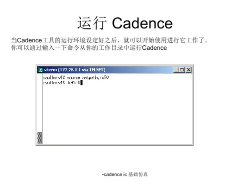
§ 1-1 进入Cadence软件包一.在工作站上使用在命令行中(提示符后,如:ZUEDA22>)键入以下命令icfb&↙(回车键),其中& 表示后台工作。
Icfb调出Cadence软件。
出现的主窗口如图1-1-1所示:图 1-1-1Candence主窗口二.在PC机上使用1)将PC机的颜色属性改为256色(这一步必须);2)打开Exceed软件,一般选用xstart软件,以下是使用步骤:start method选择REXEC(TCP-IP),Programm选择Xwindow。
Host选择10.13.71.32 或10.13.71.33。
host type选择sun。
并点击后面的按钮,在弹出菜单中选择command tool。
确认选择完毕后,点击run!3)在提示符ZDASIC22> 下键入:setenv DISPLAY 本机ip:0.0(回车)4)在命令行中(提示符后,如:ZUEDA22>)键入以下命令icfb&↙(回车键)即进入cadence中。
出现的主窗口如图1-1-1所示。
以上是使用xstart登陆cadance的方法。
在使用其他软件登陆cadance时,可能在登录前要修改文件.cshrc,方法如下:在提示符下输入如下命令:vi .cshrc↙ (进入全屏幕编辑程序vi)将光标移至setevn DISPLAY ZDASIC22:0.0 处,将“ZDASIC22”改为PC机的IP,其它不变(重新回到服务器上运行时,还需按原样改回)。
改完后存盘退出。
然后输入如下命令:source .cshrc↙ (重新载入该文件)以下介绍一下全屏幕编辑程序vi的一些使用方法:vi使用了两种状态,一是指令态(Command Mode),另一是插入态(Insert Mode)。

CAdence16.6PSpice1,使⽤⾃带例程进⾏第⼀个仿真1、建⽴原理图选择如下
2、新建⼀个⼯程,如下:
3、上图点击OK,进⼊界⾯,界⾯有下拉框,以放⼤器为例
4
5、发现⼯程⾥边⾃带如下:
6、点击1处,弹出2的参数会话框
7、点击第⼀张图,开始运⾏
8、弹出新的,运⾏结果如下:
在7界⾯更改了参数以后,只需要在8的界⾯点击运⾏就能看到新的波形了
9、可以在红圈位置直接删除不想看到的,点击选中,delete
10、点击1,在2位置添加想看到的曲线
例如看功率如下
11、如何看功率最⼤值,打击1,2处选择函数,3处选中要看的
得到结果如下
12、点击如下按钮,让此界⾯永远处于最上,之后让界⾯像第⼆张图这样
13、我们此时可以移动原理图的探针,我们会发现,波形跟着实时改变
14、⽣成报告。
window--copy to clipboard,之后在word⾥边可以直接粘贴。
15、通过点击如下按钮,能看到直流静态⼯作点、直流静态电流,功耗。
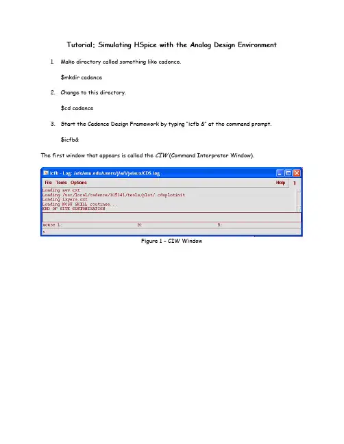
Tutorial: Simulating HSpice with the Analog Design Environment1.Make directory called something like cadence.$mkdir cadence2.Change to this directory.$cd cadence3.Start the Cadence Design Framework by typing “icfb &” at the command prompt.$icfb&The first window that appears is called the CIW (Command Interpreter Window).Figure 1 – CIW WindowAnother window that appears is the Library Manager. This window allows you to browse the available libraries and create your own.Figure 2 – Library Manager WindowIn the Library Manager, create a new library called EEE534. Select File->New->Library. This will open a new dialog window, in which you need to enter the name of your library, library path, and "Attach to existing tech library." Fill out the form as shown below, then select OK.Figure 3 – Create Library FormYou should see the library "EEE534" appear in the Library Manager.Figure 4 – Library Manager display newly created libraryNext, select the library you just created in the Library Manager and select File->New->Cell View.... We will create a schematic view of an inverter cell. Simply type in "INV" under cell-name and "schematic" under view. Click OK or hit the Enter key. Note: that the "Tool" is automatically set to "Composer-Schematic", the schematic editor.Figure 5 – Create New File FormAlternatively, you could select the "Composer-Schematic" tool, instead of typing out the view name. This will automatically set the view name to "schematic".After you hit "OK", the blank Composer screen will appear.Figure 6 – Virtuoso Schematic EditorTo generate a schematic, you will need to go through the following steps:•From the Schematic Window, choose Add->instance. The Component Browser, will then pop up.•In the Library field, select NCSU_Analog_Parts. We will place the pmos, nmos, vdd, gnd, vdc, vpulse andcap instances in the Schematic Window from the NCSU_Analog_Parts library asinstructed below.Note: pay special attention to the parameters specified in vdc, vpulse, and cap. These parameters are very important in simulation.Place pmos instance•In Component Browser, select P_Transistors and then pmos.•Place it in the Schematic WindowFigure 7 – Add pmos InstancePlace nmos instance•In Component Browser, select N_Transistors and then nmos.•Place it in the Schematic Window.Figure 8 – Add nmos InstancePlace gnd instance•In Component Browser, select Supply_Nets and then gnd.•Place it in the Schematic Window.Figure 9 – Add gnd Instance Place vdd instance•In Component Browser, select Supply_Nets and then vdd •Place it in the Schematic Window.Figure 10 – Add vdd InstancePlace IN pin•From the Schematic Window menu, select Add -> Pin...•In the Pin Name field , enter IN•In the Direction field, select input•Place it in the Schematic WindowFigure 11 – Add Input PinPlace OUT pin•From the Schematic Window menu, select Add -> Pin...•In the Pin Name field , enter OUT•In the Direction field, select output•Place it in the Schematic WindowFigure 12 – Add Output PinPlace vdc instance•In the Component Browser, select Voltage Sources and then vdc •In the DC voltage field, enter 5 V•Place it in the Schematic WindowFigure 13 – Add vdc SourcePlace vpulse instance•In the Component Browser, select Voltage_Sources and then vpulse •Enter the following values in the form:Figure 14 Edit Object vpulse SourcePlace cap instance•In Component Browser, select R_L_C and then cap•In the Capacitance field, enter OutCap F. (This Design Variable will be used in Artist.) •Place it in the Schematic WindowFigure 15 – Add cap InstancePlace wires•In the Schematic Window menu, select Add -> Wire (narrow)•Place wires to connect all the instances•Select Design -> Check and Save.Look at the CIW. You should see a message that says:Extracting “INV schematic”Schematic check completed with no errors.“EEE534 INV schematic” saved.If you do have some errors or warnings, the CIW will give a short explanation of what those errors are. Errors will also be marked on the schematic with a yellow or white box. Errors must be fixed for your circuit to simulate properly. When you find a warning it is up to you to decide if you shouldfix it or not. The most common warnings occur when there is a floating node or when there are wires that cross but are not connected. Just be sure that you know what effect each of these warning will have on your circuit when you simulate.Your schematic should look like the one shown below.Figure 16 – Completed SchematicIf you would like to learn more about the schematic editor, you can work through chapters 1-5 of the Composer Tutorial that comes with the Cadence documentation. Start the documentation browser by typingcdnshelp &at the command prompt. If you find that you cannot view the figures correctly in the web browser, you can click the View/Print PDF link at the top of the page to launch a PDF viewer for the tutorial. This documentation browser offers many more links for you to learn about the Cadence Design Framework.Simulate the Schematic with HSPICE within Virtuoso Analog Design EnvironmentSet up the Simulation EnvironmentYou are now prepared to simulate your circuit.From the Schematic Window menu, select Tools -> Analog Environment. A window will pop-up. This window is the Analog Design Environment Window.Figure 17 - Analog Design Environment WindowChoose a SimulatorFrom the Analog Design Environment menu, select Setup -> Simulator/Directory/Host. Enter the fields as shown below. Choose hspiceS as your simulator. Your simulation will run in the specified Project Directory. You may choose any valid pathname and filename that you like.Figure 18 Choosing Simulator/Directory/Host FormChoose AnalysisWe will setup to do a Transient Analysis on the circuit that we just produced.From the Analog Design Environment menu, select Analyses -> Choose... Fill out the form with the following values:Figure 19 – Choosing AnalysesAdd a VariableFrom the Analog Design Environment menu, select Variables -> Edit. The Editing Design Variables form will appear. Fill out the form as shown below, and then click Add to send this Variable to the Table of Design Variables.(Recall that we entered the OutCap Design Variable in the Capacitor component while editing the schematic in the previous section.)Figure 20 – Editing Design Variables FormSetup OutputWhen using Transient Analysis, the transient voltage will be saved automatically. We can save the current through capacitor C0 in the schematic by doing the following:From the Analog Design Environment menu, select Outputs -> To be Saved -> Select On Schematic In the Schematic Window, click on the lower terminal (not the wire) of capacitor C0.After you click on the terminal, the Analog Design Environment Window should look like this:Figure 21 Analog Design Environment WindownRun SimulationFrom the Analog Design Environment menu, select Simulation -> Run, Look at the echoing information in the CIW window. If the simulation succeeds, the window will display “...successful.”Figure 22 – CIW after simulationIf the simulation is unsuccessful, then one of the error messages should provide a clue as to what went wrong. Remember that you can move elements around in your schematic by clicking and dragging them. You can delete them by selecting them and pressing the “delete” key. You modify the properties of the elements by selecting them and pressing the “q” key.If you would like to learn more about the Analog Design Environment, select Analog Design Environment->Cadence Analog Design Environment User Guide in the cdnshelp browser window.View WaveformsFrom the Analog Design Environment menu, select Results -> Direct Plot -> Transient Signal. The Waveform Window will then pop up. In the Schematic Window, click on the IN wire and then Click on the OUT wire, then press ESC on your keyboard.The two curves (IN and OUT) will then be displayed in this window:Figure 23 – Waveform ViewerPress the Strip Chart Mode icon (4th icon from right) on the Waveform WindowThe waveforms will then be displayed separately as shown below:Figure 24 – Waveform Viewer, Strip Chart ModeIf you would like to learn more about the Waveform Viewer, select Analog Design Environment->Waveform User Guide in the cdnshelp browser window.Use CalculatorIn Analog Design Environment Window, go to Tools -> Calculator. The Calculator Window will then pop up, as shown below:Figure 25 – CalculatorIn Calculator Window, go to Options -> uncheck RPN. We are going to use the calculator to plot both the current through the capacitor and the absolute value of the capacitor current.In the Calculator Window, click on the tran tab then click the it radio button. In the Schematic Window, click on the lower terminal of the capacitor. Returning to the Calculator Window, the text area at the top should like this:Figure 26 – Calculator after selecting lower capacitor terminalIn the Calculator Window, press the plot icon to plot this waveform in the Waveform Window. In the Calculator Window, select the New Subwindow. In the Calculator Window, press the clear button to erase the text area, select abs, press the “(“ symbol and press the it radio button. In the Schematic Window, click on the lower terminal of the capacitor. Returning to the Calculator Window, press the “)” symbol, the text area at the top should like this:Figure 27 - Calculator after selecting lower capacitor terminalIn the Calculator Window, press the plot button to plot this waveform in the Waveform Window. Your Waveform Window should now look like this:Figure 28 – Waveform Display with current through the capacitor and the absolute value of thecapacitor current。

CADENCE仿真流程1.设计准备在进行仿真之前,需要准备好设计的原理图和布局图。
原理图是电路的逻辑结构图,布局图是电路的物理结构图。
此外,还需要准备好电路的模型、方程和参数等。
2.确定仿真类型根据设计需求,确定仿真类型,包括DC仿真、AC仿真、时域仿真和优化仿真等。
DC仿真用于分析直流电路参数,AC仿真用于分析交流电路参数,而时域仿真则用于分析电路的时间响应。
3.设置仿真参数根据仿真类型,设置仿真参数。
例如,在DC仿真中,需要设置电压和电流源的数值;在AC仿真中,需要设置信号源的频率和幅度;在时域仿真中,需要设置仿真的时间步长和仿真时间等。
4.模型库选择根据设计需求,选择合适的元件模型进行仿真。
CADENCE提供了大量的元件模型,如晶体管、二极管、电感、电容等。
5.确定分析类型根据仿真目标,确定分析类型,例如传输功能分析、噪声分析、频率响应分析等。
6.仿真运行在仿真运行之前,需要对电路进行布局和连线。
使用CADENCE提供的工具对电路进行布局和连线,并生成物理设计。
7.仿真结果分析仿真运行后,CADENCE会生成仿真结果。
利用CADENCE提供的分析工具对仿真结果进行分析,观察电路的性能指标。
8.优化和修改根据仿真结果,对电路进行优化和修改。
根据需要,可以调整电路的拓扑结构、参数和模型等,以改进电路的性能。
9.再次仿真和验证根据修改后的电路,再次进行仿真和验证,以确认电路的性能指标是否得到改善。
最后需要注意的是,CADENCE仿真流程并不是一成不变的,根据具体的设计需求和仿真目标,流程可能会有所调整和修改。
此外,CADENCE还提供了许多其他的工具和功能,如电路板设计、封装设计、时序分析等,可以根据需要进行使用。
CADENCE仿真步骤
Cadence是一款电路仿真软件,它可以帮助设计师创建、分析和仿真
电子电路。
本文将介绍Cadence仿真的步骤。
1.准备仿真结构:第一步是准备仿真结构。
我们需要编写表示电路的Verilog或VHDL代码,然后将它们编译到Cadence Integrated Circuit (IC) Design软件中。
这会生成许多文件,包括netlist和verilog等文件,这些文件将用于仿真。
2.定义仿真输入输出信号:接下来,我们需要定义仿真的输入信号和
输出信号。
输入信号可以是电压、电流、时间和其他可测量的变量。
我们
需要定义输入信号的模拟和数字值,以及输出信号的模拟和数字值。
3.定义参数:参数是仿真中用于定义仿真设计的变量,这些变量可以
是仿真中电路的物理参数,如电阻、电容、时延、输入电压等,也可以是
算法参数,如积分步长等。
4.运行仿真:在所有参数和信号都设置完成后,我们可以运行仿真。
在运行仿真之前,可以使用自动参数检查来检查参数是否正确。
然后,使
用“开始仿真”命令即可启动仿真进程。
5.结果分析:在仿真结束后,我们可以使用结果分析器来查看输出信
号的模拟和数字值,以及仿真中电路的其他特性,如暂态分析、稳态分析、功率分析等。
以上就是Cadence仿真步骤。

CadenceallegroPI仿真PCB中导⼊⽹表后,设置层叠结构(电源层、地层),划分好电源层,接下来:a) 将allegro切换到Allegro PCB PI option XL版本,Analysis->Preference,点开电源完整性选项卡,其中的⼀些常见选项如Min.plane/board area的值(⼩于它的平⾯仿真时直接就忽略了);b) Analysis->Power Integrity,(第⼀次建⽴会有警告,确定),接下来就是设置了,依次为:板⼦尺⼨->层叠结构->电源层的DC⽹络电压->添加电源层对(可以看到电源层对之间的内部电容)->选择仿真要⽤的的电容->选DCL(decap capacitou library,去耦电容器库)->勾选Board⽂件夹下的各电容(可以看到电容值、ESR、电感、谐振频率)->finish。
如图图1 PI设置向导完后的界⾯c) 选择需要仿真的电源层对,设置该层的纹波,最⼤的变化电流(可以看到该平⾯的⽬标阻抗)->点Single Node Simulation进⾏单节点仿真(不考虑元器件的摆放位置,验证电容的数⽬及型号是否满⾜),如图2:图2 单节点仿真图从图中可以看出,在200M频率内,⿊⾊的线为有电容之后的曲线,它位于⽬标阻抗(黄⾊)线下⾯,说明在200M的频率(⾃⼰理解为PCB 电源层给供电的IC芯⽚的频率)内,电源是完整的。
但实际情况并不⼀定是这样,如图3:图3 在单节点仿真中加实际情况如红⾊的曲线,则应为电源平⾯选⼀个电容的谐振频率为fa的电容,再次仿真之后,会得到有两个峰值的曲线,再加谐振频率等于,峰值对应的横坐标(谐振频率)的电容值即可,依次这样进⾏,直到整条曲线在要求的频率范围之内,位于⽬标谐振频率曲线下⾯。
(在调的时候,不⼀定是⾮得改原理图中电容的⼤⼩,也可适当增加原理图中滤波电容的数量)如蓝⾊曲线,相对于红⾊曲线,其谐振频率不到1M,⽅法同上,不过选这样的电容,电容值都⽐较⼤,如100uF。

cadence原理图仿真首先,我们来了解一下cadence原理图仿真的基本原理。
在进行原理图仿真时,我们需要将电路设计转换为一个数学模型,然后利用计算机软件对这个模型进行求解,得到电路的各种参数和性能指标。
这个数学模型通常是由电路的基本元件和它们之间的连接关系构成的,通过建立节点方程和元件特性方程,可以得到一个包含了电路各种参数的数学方程组。
然后利用数值计算方法对这个方程组进行求解,就可以得到电路的各种性能指标,比如电压、电流、功率等。
在cadence原理图仿真中,我们通常会使用一些常见的仿真工具,比如SPICE仿真器。
SPICE是一种通用的电路仿真工具,它可以对各种类型的电路进行仿真,包括模拟电路、混合信号电路和射频电路等。
通过建立电路的原理图,并在仿真器中设置各种参数和仿真条件,就可以对电路进行仿真分析,得到电路的各种性能指标。
在进行cadence原理图仿真时,我们需要注意一些关键的仿真参数和设置。
首先是仿真的时间步长和仿真的时间范围,这两个参数会直接影响到仿真的精度和速度。
通常情况下,我们需要根据电路的特性和仿真的要求来合理地设置这两个参数,以保证仿真结果的准确性。
另外,还需要注意仿真的激励信号和仿真的分析类型,比如直流分析、交流分析、脉冲分析等,这些参数会直接影响到仿真的结果和分析的内容。
除了基本的仿真参数设置,我们还需要注意一些特殊情况下的仿真技巧。
比如在进行混合信号电路的仿真时,需要考虑模拟部分和数字部分之间的接口和耦合关系,以保证整个系统的稳定性和正确性。
另外,在进行射频电路的仿真时,需要考虑传输线的特性和电磁场的影响,以保证仿真结果的准确性和可靠性。
总的来说,cadence原理图仿真是电子设计中非常重要的一环,它可以帮助工程师们验证电路设计的正确性和稳定性,提前发现潜在的问题,从而节省时间和成本。
通过合理地设置仿真参数和注意一些特殊情况下的仿真技巧,可以得到准确可靠的仿真结果,为电路设计和调试提供有力的支持。
Cadence仿真流程Cadence 仿真流程第⼀章在Allegro 中准备好进⾏SI 仿真的PCB 板图1)在Cadence 中进⾏SI 分析可以通过⼏种⽅式得到结果:Allegro 的PCB 画板界⾯,通过处理可以直接得到结果,或者直接以*.brd 存盘。
使⽤SpecctreQuest 打开*.brd,进⾏必要设置,通过处理直接得到结果。
这实际与上述⽅式类似,只不过是两个独⽴的模块,真正的仿真软件是下⾯的SigXplore 程序。
直接打开SigXplore 建⽴拓扑进⾏仿真。
2)从PowerPCB 转换到Allegro 格式在PowerPCb 中对已经完成的PCB 板,作如下操作:在⽂件菜单,选择Export 操作,出现File Export 窗⼝,选择ASCII 格式*.asc ⽂件格式,并指定⽂件名称和路径(图1.1)。
图1.1 在PowerPCB 中输出通⽤ASC 格式⽂件图1.2 PowerPCB 导出格式设置窗⼝点击图1.1 的保存按钮后出现图1.2 ASCII 输出定制窗⼝,在该窗⼝中,点击“Select All”项、在Expand Attributes 中选中Parts 和Nets 两项,尤其注意在Format 窗⼝只能选择PowerPCB V3.0 以下版本格式,否则Allegro 不能正确导⼊。
3)在Allegro 中导⼊*.ascPCB 板图在⽂件菜单,选择Import 操作,出现⼀个下拉菜单,在下拉菜单中选择PADS 项,出现PADS IN 设置窗⼝(图1.3),在该窗⼝中需要设置3 个必要参数:图1.3 转换阿三次⽂件参数设置窗⼝i. 在的⼀栏那填⼊源asc ⽂件的⽬录ii. 在第⼆栏指定转换必须的pads_in.ini ⽂件所在⽬录(也可将此⽂件拷⼊⼯作⽬录中,此例)iii. 指定转换后的⽂件存放⽬录然后运⾏“Run”,将在指定的⽬录中⽣成转换成功的.brd ⽂件。
CDNLive! Paper – Signal Integrity (SI) for Dual Data Rate (DDR) InterfacePrithi Ramakrishnan iDEN Subscriber Group Plantation, FlPresented atIntroductionThe need for Signal Integrity (SI) analysis for printed circuit board (PCB) design has become essential to ensure first time success of high-speed, high-density digital designs. This paper will cover the usage of Cadence’s Allegro PCB SI tool for the design of a dual data rate (DDR) memory interface in one of Motorola’s products. Specifically, this paper will describe the following key phases of the high-speed design process: Design set-up Pre-route SI analysis Constraint-driven routing Post-route SI analysisDDR interfaces, being source synchronous in nature, feature skew as the fundamental parameter to manage in order to meet setup and hold timing margins. A brief overview of source synchronous signaling and its challenges is also presented to provide context.Project BackgroundThis paper is based on the design of a DDR interface in an iDEN Subscriber Group phone that uses the mobile Linux Java platform. The phone is currently in the final stages of system and factory testing, and is due to be released in the market at the end of August 2007 for Nextel international customers. The phone has a dual-core custom processor with an application processor (ARM 11) and a baseband processor (StarCore) running at 400MHz and 208MHz respectively. The processor has a NAND and DDR controller, both supporting 16-bit interfaces. The memory device used is a multi-chip package (MCP) with stacked NAND (512Mb) and DDR (512Mb) parts. The NAND device is run at 22MHz and the DDR at 133MHz. The interface had to be supported over several memory vendors, and consequently had to account for the difference in timing margins, input capacitances, and buffer drive strengths between different dies and packages. As customer preference for smaller and thinner phones grows, the design and placement of critical components and modules has become more challenging. In addition to incorporating various sections such as Radio Frequency (RF), Power Management, DC, Audio, Digital ICs, and sub-circuits of these modules, design engineers must simultaneously satisfy the rigid placement requirements for components such as speakers, antennas, displays, and cameras. As such, there are very few options and little flexibility in terms of placement of the components. This problem was further accentuated by the fact that several layers of the 10 layer board (3-4-3 structure with one ground plane and no power planes) were reserved for power, audio, and other high frequency (RF) nets, leaving engineers with few layers to choose from for digital circuitry.Figure 1. Memory Interface routes With the DDR interface data switching at 266MHz, we had very tight margins — 600ps for data/DQS lines, 280ps for the address lines, and 180ps for control lines. However, with the NAND interface we had larger margins that were on the order of a few tens of nanoseconds. In these situations, choosing a higher drive strength and using terminators of appropriate values (to meet rise times and avoid overshoot/undershoot) has become a common practice in DDR designs. However, due to the lack of space on the board, we were not in a position to use terminators. Therefore, we used programmable buffers on our processor, and with the help of Cadence SI tools were able to fine-tune the design. Our group migrated from using Mentor Graphics to Cadence SI during this project. As one might expect, this made the task of designing a high speed DDR interface even more challenging. To help overcome this, we worked extensively with Cadence Services, where Ken Willis supported us on the SI portion of the design.The Source Synchronous Design ChallengeBefore discussing the specifics of the Motorola DDR interface, a brief overview of source synchronous signaling is provided here for context. Historically, digital interfaces have utilized “common clock” signaling, as shown in the figure below.Clock DriverTcoInterconnect Delay D0 D1 D2 D0 D1 D2DriveReceiveFigure 2. Common clock designWith common clock interfaces, the clock signal is provided to the driving and receiving components from an external component. The magnitude of the driver’s Tco (time from clock to output valid) and the interconnect delay between the driving and receiving components becomes a limiting factor in the timing of the interface. From a practical standpoint, it becomes increasingly challenging to implement interfaces of this type above several hundred megahertz. In order to accommodate requirements for faster data rates, source synchronous signaling emerged as the new paradigm. This is illustrated in the figure below.StrobeD 0 D 1D 0 D 1DriveReceiveFigure 3. Source synchronous design.In a source synchronous interface, the “clock” is provided locally by the driving component, and is generally called a “strobe” signal. The relationship between the strobe and its associated data bits is known as it leaves the driving component, with setup and hold margins pre-established as the signals are put onto the bus.TsetupTholdFigure 4. Timing diagram. This essentially takes the driver’s Tco as well as the magnitude of the interconnect delay between the driving and receiving chip out of the timing equation altogether. The timing challenge then becomes to manage the skew between the data and strobe signals such that the setup and hold requirements at the receiving end are still met.Technical ApproachThe general technical approach used in this project can be broken down into the following key phases of the high-speed design process: Design set-up Pre-route SI analysis Constraint-driven routing Post-route SI analysisFirst the PCB design database is set up to enable analysis with Allegro PCB SI. Before routing is performed, initial trade-offs are examined at the placement stage, and constraints are captured to facilitate constraint-driven routing. When routing is completed, detailed analysis is performed, interconnect delays extracted, and setup/hold margins are computed. Any adjustments required are fed back to the layout designer, and the postroute analysis is repeated. This basic process is diagrammed below.Design Setup SI Models Pre-Route AnalysisStartConstraints RoutingPost-Route AnalysisnoMargins OK?yes EndFigure 5. SI design process flow. Detail on the major design phases are provided in the subsequent sections. Design Setup By virtue of its direct integration with the Allegro PCB layout database, Allegro SI analysis requires that the design be set up to facilitate the automated extraction, circuit building, netlisting, simulation, and analysis that it performs. This essentially means adding the needed intelligence to the physical Allegro database that allows the tool to do its job. This setup involves the following: Cross section DC nets Device definitions SI models By definition, SI analysis involves the modeling of interconnect parasitics. In order to do this accurately, the tool needs to know the properties and characteristics of the materials used in the PCB stack-up. This information is defined in the Cross Section form, as shown below.It is crucial to get this data correct, as it will be fed to the 2D field solver to model interconnect parasitics during the extraction process. The best source for this detailed information is generally from the PCB fabricator. Layer thickness, dielectric constant, and loss tangent are all critical parameters for the cross section definition. In order for circuit extraction to be done properly, the tool needs to know about DC nets in the design, and what their associated voltage levels are. This accomplishes two main things in the setup; a) enables voltage sources to be injected properly in the extracted circuits, and b) avoids having the tool needlessly trying to extract extremely large DC nets, and hanging up the analysis process. Take the example of a parallel resistor termination. Allegro SI will encounter the resistor as it walks the signal net to be extracted. The tool will look up the SI model assigned to this resistor, splice in the resistor subcircuit, and continue extracting whatever is on the other side of the resistor. If this is a large DC net (ex. VTT), the desire is for the tool to put a voltage source at the 2nd resistor pin, complete the circuit, and simulate the signal. To do this properly, the tool relies on a VOLTAGE property to exist on the DC net, with a numeric value defined. In the absence of the VOLTAGE property, the tool will simply continue to extract, which in the case of a 2000 pin ground net, would be a large waste of computational time. To identify DC nets, clicking “Logic > Identify DC Nets” will spawn the following form.All DC nets in the design should be identified, to fully optimize SI analysis. These can be identified up front in the schematic, as well as in the physical layout as shown here. The next step in the design set-up process is to verify that the logical “CLASS” and “PINUSE” attributes for the devices in the design are defined appropriately. These attributes originate from the schematic symbol libraries and are passed into the Allegro physical layout environment. In an ideal methodology, these libraries would be defined properly and would require no edits. However, this is not always the case, and as these attributes have a bearing on the behavior of the SI analysis, it is worth mention here. The “CLASS” attribute is used to distinguish between different types of components in the PCB design. Legal values of “CLASS” are listed below: IC – This is used for digital integrated circuits, which contain drivers and/or receivers. These types of components are modeled with an SI model of the type “IbisDevice”. When the automated circuit building algorithms in Allegro PCB SI encounter a model of this type, it looks up the buffer model (driver, receiver, or bidirectional) assigned to the pin in question, and inserts it into the circuit along with its associated package parasitics. IO – A component with CLASS = IO is intended for components that connect off-card to other physical layout designs, such as connectors. These components can be associated with a “DesignLink”, which provides netlisting to other physical designs and enables multi-board SI analysis. So circuit building algorithms expect to jump from a device of CLASS=IO to a similar device on a different physical layout. DISCRETE – For devices of this class, circuit building algorithms expect to traverse “through” the component, from one pin to another, inserting a subcircuit in-between. A good example of this would be a series resistor.If CLASS attributes are not set up properly in the source schematic libraries, they can be edited in the physical layout database for analysis by using the form shown below, launched from the “Logic > Parts List” menu pick.The “PINUSE” attribute also impacts the behavior of the SI analysis, as the tool uses this information to determine if a pin is a driver, receiver, bidirectional, or passive pin. As with the “CLASS” attribute, in an ideal methodology this is defined properly in the schematic libraries, and no editing is required in physical layout. “PINUSE” can be modified in two main ways for SI purposes. The most straightforward way is to ensure that the IOCell models used in the IbisDevice models assigned to components have the appropriate Model Type for the signals they are associated to. When SI models are assigned to components, the tool will check for conflicts between the model and the PINUSE it finds for the component in the design, and will use the SI model to automatically override the PINUSE found in the drawing. So if the correct pin types are found in the SI models, the layout will automatically inherit those settings. For components not explicitly modeled, their PINUSE can be set using the form shown below, launched from the “Logic > Pin Type” menu pick.Signal Integrity (SI) models can be assigned using the “Signal Model Assignment” form, shown below.Upon clicking “OK” the selected models will be assigned to the components and saved directly in the layout database. As mentioned previously, “PINUSE” attributes will be synced up, with the SI models superseding attributes in the original layout drawing.Pre-Route SI AnalysisPerforming pre-route analysis is a key part of the high-speed design process. Once critical component placement has been done, Manhattan distances can be used to estimate trace lengths, and can provide a realistic picture of how routed interconnect will potentially perform.Before simulations are run for critical signals, the timing of the interface must be well understood. To accomplish this, we will first sketch timing diagrams for each signal group and then extract a representative signal for analysis. Next, we will explore Z0, layer assignments, drive strength, route lengths, spacing, and terminations for these nets.To sketch the timing diagrams, we first analyze the memory interface. The memory interface consists of both DDR and NAND signals and has around seventy nets. To simplify the analysis of the interface, we first divide these nets based on function and then simulate one net from each group. Accordingly, we select one signal from each of the following groups —clock_ddr, strobe_ddr , data_ddr, control_ddr, address_ddr, control_nand, and data_nand — for our pre-route simulations.To understand the timing relations in the interface, we should look at the following operations between the memory device and the processor — read, write, address write, and control operations. Next, we identify the nets involved and the clocking reference signal for each of these operations. We then calculate the worst case slack available from the setup and hold numbers available in the data sheets. In particular, we adopted the worst case numbers across four different memory vendors, to ensure robustness of the manfactured system in the field..1.ReadDuring the read operation, the memory drives the data and DQS lines. The processor has a delay line (a series of buffers which can be tapped at different points), which is used to delay the DQS signal so that it samples the data at quarter of the cycle. The processor also offers programming options that allow us to apply an offset to the quarter cycle, enabling us to meet our setup and hold times. Hence, the processor self-corrects forstrobe/data skew using this delay line. The granularity of this delay line is 30 ps; that is, each of the buffers of the delay line contributes 30 ps of delay. The data lines 0-7 are clocked with respect to the DQS0 strobe signal, and the data lines 8-15 are clocked with respect to DQS1. Data and strobe lines should be clustered, with the matching constraints determined by the write cycle.2.WriteFigure 7. Write operation at memory interface.During the write operation, both data and DQS are driven by the processor. Data is latched at both the positive and the negative edges of the DQS signals. Here again, data bits 0-7 are clocked by DQS0 and data bits 8-15 are clocked by DQS1. The setup and hold times available as these signals come out of the DDR controller are 1.58ns and 1.7ns respectively and the corresponding times required at the memory to ensure correct operation is 0.9ns. Hence, the slack available for routing is the lesser of 1.58ns – 0.9ns or 1.7ns – 0.9ns, which comes out to be 0.68ns. This amounts to an allowable ~85mm mismatch between the data lines. In addition, we need to make sure that length of the DQS lines is around the average of all the data lines. The data mask signals DQM0 and DQM1 also come into play during the write operation and we should group them along with the respective data lines.3.Address busFigure 8. Address bus operation at memory interface.Both address and clock lines are driven by the processor. The address bits 0-12 are clocked by the differential clock and latched at the positive edge of the clock. The setup and hold times available for these signals from the DDR controller are 1.78ns and 4.22ns respectively and the corresponding times required at the memory to ensure correct operation is 1.5ns for both. Hence the worst case slack for routing is 0.28ns and we have to try to match our signals to meet these numbers. The 0.28ns slack amounts to ~14mm mismatch between the address lines and the clock.4.Control linesFigure 9. Control lines at memory interface.The control signals are clocked by the differential clock and latched at the positive edge of the clock. The setup and hold times coming out of the DDR controller are 1.64ns and 4.04ns respectively. The setup and hold times required at the memory to ensure correct operation is 1.5ns. Hence, the worst case slack for routing is 0.14ns and we have to try and match our signals to meet these numbers. The 0.14 ns slack amounts to ~7mm mismatch between the control lines and the clock.In addition, CLK to DQS skew is around 600 ps. With regards to the NAND lines, setup and hold numbers are in the order of tens of ns and hence routing them as short as possible based on their Manhattan lengths would suffice.To complete pre-route analysis, SigXplorer must be setup for these tasks:a. Extract a topology file for single net analysis. To bring up the net in SigXplorer, it is essential that the models are assigned, as described in Section 2, to each of the drivers, receivers, and components in the signal path.b. Set up parameters for extraction and simulate using SigXplorer.c. Perform measurements using SigWaveThe following screenshots of SigXplorer show this process in detail.Figure 10. SigXplorer screenshots.Since at this point none of the nets in the design are routed we need to set the percent Manhattan section for unrouted interconnect models. We should then select the net, as shown in the next screenshot, for analysis.Analyze Æ SI/EMI Sim Æ PreferencesThe speed at which the signal travels in the trace, where C is 3 x 10⁸ m/s and E reff is the effective dielectric constant seen in the interconnectSets the default lengthfor unrouted transmission linesAt this point, it is important to check if your driver and receiver pins are set correctly. The net chosen in the above example is a data net, it is bi-directional, hence it can be driven both by the memory device as well as the processor. The view topology icon can be clicked to export this net in SigXplorer.The tool extracts the net along with drivers, receivers and strip lines on various layers of the board. Before you start the simulation, you must set the stimulus frequency, pulse step offset, and cycle count. This can be set in the following GUI.Analyze Æ PreferencesBoth the memory device and the processor have programmable drive strengths. The buffer model can bechanged to pick up the various drive strengths that are available in the dml models of the devices till we observe satisfactory waveforms in SigWave.Analyze Æ SI/EMI Sim Æprobeinvokes SigXplorerMake sure you check you driver and load pinsSigXplorer allows you to sweep any of the parameters such as the thickness, length, drive strengths and displays corresponding settle/switch delays, monotonicity, and glitch tolerance for the corresponding simulation. It also allows adding components such as resistors and capacitors and let’s us sweep their values. We added a resistor in series with our clock in or to get rid of ringing in the rising edge. The tool let us determine what values were suitable for this resistor. As shown in the next figure the waveform corresponding to our simulation can bebrought up on SigWave.driverreceiverYou can observe the rise/fall times, look for noise margins, overshoot/undershoot of the receiver waveform. The constraints we develop in the pre-route simulation will be used by the routing tool to ensure correct first time results. This leads to our next section; Constraint-driven routing.Constraint-driven routingOnce pre-route analysis has been done, and trade-offs have been examined, signal wiring constraints need to be developed to drive the constraint-driven routing process. With the DDR interface being point-to-point between the processor and memory, we translated our timing requirements into length constraints to make the routing as straightforward as possible. We also assigned layer constraints for our DDR signals. Both the length and the layer constraints can be directly applied to the constraint manager before the routing process starts.For our particular design, we determined the following layer assignments from the results of the pre-route simulations, taking into account the layer’s characteristic impedance per our stack-up:Layer 6 Æ ground planeLayer 7 Æ clock, add, ctrlLayer 8 Æ data, strobeLayer 9 Æ NAND interfaceBefore we set up our design for auto-routing, we routed the differential clock lines manually on the layers closest to the ground plane. For the rest of the nets, the layer constraints can be created as shown in the following snapshots of the constraint manager.Electrical Constraint Set Æ WiringRight click on board Æ Create new constraintName the constraint (ex. ECSET1)We choose one layer with horizontal orientation and one with vertical for each of our layer sets. You can form groups from the available layer sets and create a new constraint. This constraint, which we define as ECSET1, can be easily read back in the constraint manager and applied to the relevant net group, as shown in the following snapshot.We determined from pre-route analysis the slack available for each of our net groups; however, before we translate these into length constraints it is important to get a report of the Manhattan lengths of each of these signals. To illustrate this, we will focus on the address signals. The Manhattan report of the address lines showed that the shortest lines were 6mm and the longest were 17mm. Accordingly, the minimum length constraint must be longer than 6mm and the maximum length constraint must be longer than 17mm. Additionally, from our timing diagrams, we determined that the maximum spread can be no more than 14mm. Following these restrictions, we set the minimum and maximum length limits for the address line are 11.99 mmto 18.99 mm (shown in the constraint editor window below). Based on the layout designer's recommendations, we were able to constrain a bit tighter (7mm margin) and produce better margins.To enter the length constraint, we open the Net Æ Routing ÆTotal etch length section of the constrain manager. We followed this procedure for all the other net groups. The snapshot that follows shows length constraints associated with the address lines. Here, the key is to not to over-constrain your design, but at the same time have enough constraints so the timing and signal integrity parameters are met. Over-constraining the design severely inhibits the auto-router and may leave large portions of the design (as much as 90%) un-routed.Post-Route SI AnalysisOnce the design is fully routed, detailed simulations can be run for post-route verification. The goal at this phase is to determine final margins over all corners, and find and correct any SI or timing-related issues before the board is released for fabrication. Before starting simulation, it is important to verify that the design is properly routed and that it meets the specifications/constraints. In particular, it is essential to verify that the design does not include dangling and partially-routed/un-routed nets. We must also verify that all the nets meet the length constraints assigned to them. The Constraint Manager window helps identify nets that are in violation (shown in red) and nets that are in compliance (in green). For convenience and clarity, the Constraint Manager also reports the actual route length and the Manhattan lengths for each net.The next step is to bring up the physical layout and visually inspect the nets to ensure that each net is routed in its appropriate layer, or run DRCs if the signals were explicitly limited to specific layers in Physical Constraint Sets. When test points are associated with a net, we must manually verify that the points are in line with the nets (and are not stubs hanging off the nets). Note that when using the simpler Total_Etch_Length constraint, the auto-router can meet routing length constraints for the net, even when there are stubs in the design. These stubs can produce undesirable effects such as reflections and hence this step is important. If there are too manycritical signals to check manually on larger designs, this check can be automated by using an explicit topology and stub length constraints. After manual inspection, we begin post–route simulation and generate reports to analyze the design. We then export the reports to an Excel spreadsheet to facilitate analysis.We generated both delay and reflection reports. The delay report provides information on timing parameters such as propagation delay, switch and settle rise and fall times. The reflection report presents data on signal integrity parameters such as overshoot, undershoot, noise margin, monotonicity, and glitch. Preparing the design for post-route simulation involves the selection of various options in the SI\EMI Sim preferences list. The following screen display describes this process.In the form above, we set up the frequency of the stimulus and the duty cycle. We also set up V meas as thereference for delay calculations. Choosing the reference as V meas , rather than V IH and V IL , makes analysis much easier and is in accordance with the memory datasheet. We chose V meas as 0.9V which is half of the peak-to-peak voltage swing (1.8V).Now that the design is routed, we need to set the parameters for routed interconnects. Here you can specify the minimum coupling distance for nets for the tool to recognize it as a differential pair. This can be done by invoking Analyze Æ SI ÆPref ÆInterconnect Models.Analyze Æ SI/EMI Sim Æ preferencesThe preceding screenshot shows the option that allows us to select the delay and reflection reports. In this form, we also choose all three simulation modes — fast, typical, and slow — to cover all corner cases. In our experience, running typical mode simulations were not enough to determine final timing margins over process, voltage, and temperature. So, we exported the reports to an Excel spread sheet and analyzed the results. Reflection and delay reports simulate only a primary net and none of its neighbors. As a result, these reports do not take into consideration the parasitics of the power and ground pins.Timing > Control typNote:All timings in ns unless labelled otherwise.Component Timingdriving to MemoryTsetup 1.64Tsetup 1.5Thold 4.04Thold 1.5Skew_max = 1.64 - 1.5 = 140ps between clock and controlSkew_max=0.14Clock/Strobe RelationshipsSdram_Ctrl<6:7> is differential clockInterconnect TimingXNet Drvr Rcvr PropDly SettleRise SettleFall AvgSettleSDRAM_CTRL<6>U800 V2_UU2164 C7_U2160.142029 1.13851 1.20538 1.172XNet Drvr Rcvr PropDly SettleRise SettleFall MinSettle MaxSettle MinSettleSkew MaxSettleSkew MaxSkew MarginSDRAM_CTRL<0>U800U21640.1118 1.191 1.235 1.104 1.2350.0680.0630.0680.072SDRAM_CTRL<10>U800U21640.1254 1.165 1.207SDRAM_CTRL<11>U800U21640.1114 1.141 1.187SDRAM_CTRL<12>U800U21640.1217 1.178 1.221SDRAM_CTRL<13>U800U21640.1067 1.114 1.153SDRAM_CTRL<14>U800U21640.09823 1.104 1.143SDRAM_CTRL<2>U800U21640.1274 1.163 1.205SDRAM_CTRL<3>U800U21640.09163 1.108 1.153SDRAM_CTRL<8>U800U21640.1081 1.137 1.182SDRAM_CTRL<4>U800U21640.06959 1.143 1.247SDRAM_CTRL<5>U800U21640.0862 1.169 1.285The preceding spreadsheet was created with data from delay reports and was used to analyze the control lines with respect to the clock. The clock signal in our design is called SDRAM_CTRL<6>. The sheet also lists the driver (U800, the processor), receiver (U2164, memory device), propagation delay (0.142029 ns), settle rise (1.13851 ns), and settle fall (1.20538 ns) values. The average settle delay (1.172 ns) is calculated by averaging the settle rise and settle fall numbers.The control nets SDRAM<0> to SDRAM_CTRL <14> are listed next to the corresponding drivers, receivers, propagation delays, settle rise and settle fall delays. We then look for the minimum and maximum delays of all the settle rise and settle fall delays. These are listed under maximum settle delay (1.235 ns) and minimum settle delay (1.104 ns) respectively. Using these numbers, we calculate the maximum settle skew (0.063 ns), which is the difference between the maximum settle delay (1.235ns) and the average settle time (1.172 ns) of the clock signal. We also calculate the minimum settle skew (0.063 ns), which is the difference between the minimum settle delay (1.104ns) and the average settle time (1.172 ns) of the clock signal. Subtracting the maximum of these two skews, which in our case is 0.068 ns, from the total skew available (0.140 ns) gives the margin (0.072 ns) for these nets.。
cadence原理图仿真
在进行Cadence原理图仿真时,我们需要注意以下几点,以确保仿真结果的准确性和可靠性:
1. 确认所使用的元件符合仿真要求,并正确地添加到原理图中。
这包括在仿真库中选择合适的元件模型,并将其与其他元件正确地连接起来。
2. 确认仿真的电源和接地连接正确无误。
确保电源和地线的连接不会导致任何不良影响,如电压下降或噪声干扰。
3. 设置仿真参数,如仿真时间、仿真步长等。
根据所需的仿真精度和仿真效率,选择适当的仿真参数。
4. 进行信号源的设置。
这包括选择合适的信号源类型(如AC
信号、脉冲信号等)、设置信号源的频率和振幅等参数。
5. 添加测量器件,以便在仿真过程中监测所需的电压或电流。
这些测量器件可以是电压表、电流表或示波器等。
6. 设置仿真分析类型。
根据需要进行直流分析、交流分析或者是时域分析等。
选择适当的仿真分析类型以获得所需的结果。
7. 运行仿真并分析结果。
运行仿真过程,等待仿真完成后,通过分析仿真结果来获取我们所需的电压、电流或其他信号参数。
通过遵循以上步骤,我们可以在Cadence中进行原理图仿真,并获取准确可靠的仿真结果,以验证电路设计的正确性和性能。
实验名称:模拟电路板图设计实验者:赵静怡学号:1028401083指导老师:顾江敏实验目的:1、根据已知电路图了解模拟电路设计要求2、完成模拟电路仿真,学会加载已知数据3、绘制模拟电路板图,通过DRC以及LVS检查。
进一步熟悉和掌握cadence软件的使用实验操作介绍:一、进入操作界面1、双击“VMware Workststion”,进入虚拟机。
选择用户名“icl2012”,键入密码“Su64zhouicl”进入cadence界面。
右击“Open in Terminal”进入输入指令界面。
2、部分指令说明:ls(回车)——查找当前目录下所有文件,绿色是可执行文件、蓝色为文件夹ls—l(回车)——给出文家属性、建立时间等信息cd ..(回车)——回到icl2012./ic【Tab】(回车)——打开界面二、库管理器1、点击“library manager”,打开库管理器。
认识Schematic、layout、Symbol等每一项内容。
点击左上角“show Categories”即可看到library中的具体分类。
2、点击“File—New—library”,新建一个库。
选择“Attach to an existing techfile”与pdk一致。
“Technology Library”中选择与之匹配的库。
3、建立cell,注意名字中不要有空格、只能有字母、数字、下划线。
三、绘制Schematic1、快捷键“i”:Add Instance2、快捷键“m”:移动元器件3、快捷键“w”:连线4、快捷键“l”:标注网络名5、快捷键“p”:加port6、电路仿真四、生成Symbol1、点击“Design—Create Cell view—From Cell view”生成Symbol2、绘制完成之后“Design—Check and Save”五、绘制layout1、快捷键说明:Shift+z:缩小Ctrl+z:缩小NPLUS+NV:是指只看NPLUS这一层F:刷新Q:设置参数Ctrl+d:取消所有选中Ctrl+a:全部选中Shift+k:删除标尺K:进行标尺P:布置金属线Shift+c:删除2、从电路图生成layout(1)Tools—Design—Layout XL(2)Connectivity—Update—Components and Nets从电路图更新到layout(3)将I/O Pins修改为金属1,将Pin Label Shape修改为Label,修改Pin Label Options的参量。
Cadence板级仿真Cadence的SQ仿真用于单板网络的拓扑提取或者信号质量仿真非常方便,即板级的仿真。
但随着系统的复杂,板间的信号仿真越来越多,这就涉及到两块电路板的系统级仿真。
两块PCB之间必然是通过connector连接在一起的,如果近似地处理,可以把connector当作是一根短的传输线,连接connector的两个对应网络分布在两块PCB中,我们可以分开处理,对两个网络进行分别提取,然后利用SigXplorer的Append功能进行Top整合,中间connector采用传输线近似。
这是最简单的方法。
当然还有另一种比较正式一点的方法,SQ本身就支持两块电路板的同步仿真,其原理与Xnet 的网络拓扑结构提取相当。
比如,如果我们不指定Xnet时,进行网络提取只能提取单根网络,当指定了Xnet之后,Probe提取出的网络就是Xnet,这里Xnet的指定就是给对应的无源元件,比如电阻、电容、电感等,分配Espice模型。
当然这里这里也包括连接器,只不过这比他们要稍微复杂一些。
下面就以一个例子来说明板级仿真的网络提取。
准备工作:仿真文件:cpu.brdmainboard.brd仿真模型:8347_tbga_rev203.dmlpca9548a_3_3v.dml仿真原理图:cpu.dsnmainboard.dsn拓扑结构简易视图如下:CPU端:Mainboard端:Analyze----SI/EMI Sim----Library...在Brower界面Add existing library,把需要的IC model放进去进行IC模型分配,Analyze----SI/EMI Sim----Model...在弹出的Signal Model Assignment里进行模型分配,默认的分配环境是Devices在这里进行模型分配,选中状态时,pcb界面的对应元件会临时高亮选中需要分配模型的Devices后,点击下面的Find Model,在Model Type Filter中选择IbisDevice,Model Name Pattern中输入“*”,选择正确的Model Name后模型就自动分配给对应的IC了分配好model后的devices这里不仅要给IC分配好模型,还需要给拓扑结构中的无源元件建立模型,比如这里的上拉电阻。
CADENCE仿真步骤1.电路设计:首先,需要使用电路设计软件(例如OrCAD)绘制电路原理图。
在设计电路时,应该合理选择电路元件,确保其参数和规格满足设计要求。
2.创建电路网络:在CADENCE中创建电路网络是第一步。
通过将电路原理图导入到CADENCE中,可以建立电路的模型。
在建立电路网络时,应定义元件的参数值,并将其连接起来。
3.定义仿真设置:在进行仿真之前,需要设置仿真参数。
这些参数包括仿真类型(例如直流、交流、蒙特卡罗等)、仿真步长、仿真时间等。
此外,还可以设置其他参数,如故障分析、参数扫描等。
4. 运行仿真:设置好仿真参数后,可以开始运行仿真了。
CADENCE 提供了多种仿真工具,如PSpice、Spectre等,可以根据不同的需求选择适合的工具。
在仿真过程中,CADENCE会使用电路元件的模型计算电路参数,根据仿真设置提供的信息生成相应的结果。
5.分析仿真结果:一旦仿真完成,CADENCE会生成仿真结果文件。
通过分析仿真结果,可以评估电路设计的性能。
常见的仿真结果包括电流、电压、功耗、频率响应等。
可以将仿真结果与预期结果进行比较,找出设计中的问题并进行优化。
6.优化电路设计:根据仿真结果,可以对电路设计进行调整和优化。
优化可以包括选择不同的元件、调整元件参数、改变电路拓扑等。
通过不断迭代仿真和优化,可以逐步改进电路设计,使其达到预期的性能指标。
7.验证仿真结果:当设计经过一系列的优化后,需要验证仿真结果是否可靠。
一种常用的验证方法是进行物理验证,即将最终的电路设计制作出来并测量其实际性能。
通过比较实际测量结果与仿真结果,可以验证仿真的准确性,并进行必要的修正。
8. 导出设计文件:一旦电路设计完成并验证通过,就可以将设计文件导出,准备进一步的生产制造。
将设计文件导出为标准的格式(如Gerber文件),可以将其发送给制造商进行生产。
总结:CADENCE仿真步骤包括电路设计、创建电路网络、定义仿真设置、运行仿真、分析仿真结果、优化电路设计、验证仿真结果和导出设计文件。
矿产资源开发利用方案编写内容要求及审查大纲
矿产资源开发利用方案编写内容要求及《矿产资源开发利用方案》审查大纲一、概述
㈠矿区位置、隶属关系和企业性质。
如为改扩建矿山, 应说明矿山现状、
特点及存在的主要问题。
㈡编制依据
(1简述项目前期工作进展情况及与有关方面对项目的意向性协议情况。
(2 列出开发利用方案编制所依据的主要基础性资料的名称。
如经储量管理部门认定的矿区地质勘探报告、选矿试验报告、加工利用试验报告、工程地质初评资料、矿区水文资料和供水资料等。
对改、扩建矿山应有生产实际资料, 如矿山总平面现状图、矿床开拓系统图、采场现状图和主要采选设备清单等。
二、矿产品需求现状和预测
㈠该矿产在国内需求情况和市场供应情况
1、矿产品现状及加工利用趋向。
2、国内近、远期的需求量及主要销向预测。
㈡产品价格分析
1、国内矿产品价格现状。
2、矿产品价格稳定性及变化趋势。
三、矿产资源概况
㈠矿区总体概况
1、矿区总体规划情况。
2、矿区矿产资源概况。
3、该设计与矿区总体开发的关系。
㈡该设计项目的资源概况
1、矿床地质及构造特征。
2、矿床开采技术条件及水文地质条件。