Two or three shunt resistor based current sensing circuit design in 3-phase inverters
- 格式:pdf
- 大小:1.17 MB
- 文档页数:14
Texas Instruments, Inc. C2000 Systems and Applications2012Digital Motor ControlSoftware Library: F2803x DriversContentsINTRODUCTION (3)ADC_ILEG_DRV (4)BLDC_PWM_DRV (6)CAP_EVENT_DRV (11)DATALOG (14)HALL3_DRV (19)PWMDAC_DRV (26)PWMDRV (30)QEP_DRV (33)IntroductionThe digital motor control library is composed of C functions (or macros) developed for C2000 motor control users. These modules are represented as modular blocks in C2000 literature in order to explain system-level block diagrams clearly by means of software modularity. The DMC library modules cover nearly all of the target-independent mathematical macros and target-specific peripheral configuration macros, which are essential for motor control. These modules can be classified as:Transformation and Observer Modules Clarke, Park, Phase Voltage Calculation, Sliding Mode Observer, BEMF Commutation, Direct Flux Estimator, Speed Calculators and Estimators, Position Calculators and Estimators etc.Signal Generators and Control Modules PID, Commutation Trigger Generator, V/f Controller, Impulse Generator, Mod 6 Counter, Slew Rate Controllers, Sawtooth & Ramp generators, Space Vector Generators etc.Peripheral Drivers PWM abstraction for multiple topologies and techniques, ADC Drivers,Hall Sensor Driver, QEP Driver, CAP Driver etc.Real-Time Debugging Modules DLOG module for CCS graph window utility, PWMDAC module for monitoring the control variables through socilloscopeIn the DMC library, each module is separately documented with source code, use, and background technical theory. All DMC modules allow users to quickly build, or customize their own systems. The library supports three principal motor types (induction motor, BLDC and PM motors) but is not limited to these motors.The DMC library components have been used by TI to provide system-level motor control examples. In the motor control code, all DMC library modules are initialized according to the system specific parameters, and the modules are inter-connected to each other. At run-time the modules are called in order. Each motor control system is built using an incremental build approach, which allows some sections of the code to be built at a time, so that the developer can verify each section of the application one step at a time. This is critical in real-time control applications, where so many different variables can affect the system, and where many different motor parameters need to be tuned.Software LibraryADC Driver Description This module allows the user to configure analog-to-digital conversion (ADC) channels. The conversions are triggered on end of conversion (EOC) which is setto 4th conversion by default. In DMC projects, the converted results representload currents and DC-bus voltage but not limited to these.Availability C interface versionModule Properties Type: Target Dependent, Application IndependentTarget Devices: 28x Fixed PointC Version File Names: f2803xileg_vdc.h (for x2803x)IQmath library files for C: N/AC InterfaceC InterfaceModule UsageInstantiationThere is no instantiation for ADC configuration.Initialization// Default ADC initializationint ChSel[16] = Default_ch_sel; int TrigSel[16] = Default_trig_sel;int ACQPS[16] = Default_ACQPS;whereChSel [ ] stores which ADC pin is used for conversion when a Start of Conversion (SOC) trigger is received for the respective channelTrigSel [ ] stores what trigger input starts the conversion of the respective channelACQPS [ ] stores the acquisition window size used for the respective channelInvoking the computation macro ChSel[0]=x; ChSel[1]=y;ChSel[2]=z;Examplemain() { ChSel[1]=1; // ChSelect: ADC A1-> Phase A Current ChSel[2]=9; // ChSelect: ADC B1-> Phase B Current ChSel[3]=3; // ChSelect: ADC A3-> Phase C Current ChSel[7]=10; // ChSelect: ADC B2-> DC Bus Voltage ADC_MACRO_INIT(ChSel,TrigSel,ACQPS) // Call init macro for ADC INIT }void interrupt periodic_interrupt_isr() {clarke1.As = _IQmpy2(_IQ12toIQ(AdcResult.ADCRESULT1)-offsetA); // Phase A curr. clarke1.Bs = _IQmpy2(_IQ12toIQ(AdcResult.ADCRESULT2)-offsetB); // Phase B curr. volt1.DcBusVolt = _IQ12toIQ(AdcResult.ADCRESULT7); // DC Bus voltage meas. }Description This module generates the 6 switching states of a 3-ph power inverter used to drive a 3-ph BLDC motor. These switching states are determined by the inputvariable CmtnPointer. The module also controls the PWM duty cycle bycalculating appropriate values for the compare registers. The duty cycle valuesfor the PWM outputs are determined by the input DutyFunc.Availability C interface versionModule Properties Type: Target Dependent, Application IndependentTarget Devices: 28x Fixed PointIQmath library files for C: IQmathLib.h, IQmath.libC Version File Names: f2803xbldcpwm.h (for x2803x)C InterfaceObject DefinitionThe structure of PWMGEN object is defined by following structure definitiontypedef struct { Uint16 CmtnPointer; // Input: Commutation (or switching) state pointer input (Q0) int16 MfuncPeriod; // Input: Duty ratio of the PWM outputs (Q15)Uint16 PeriodMax; // Parameter: Maximum period (Q0)int16 DutyFunc; // Input: PWM period modulation input (Q15)Uint16 PwmActive; // Parameter: 0 = active low, 1 = active high (0 or 1)} PWMGEN;Special Constants and Data typesPWMGENThe module definition is created as a data type. This makes it convenient to instance an interface to the PWMGEN driver. To create multiple instances of the module simply declare variables oftype PWMGEN.PWMGEN_DEFAULTSStructure symbolic constant to initialize PWMGEN module. This provides the initial values to theThis default definition of the object implements two methods – the initialization and the runtime compute macro for PWMGEN generation. This is implemented by means of a macro pointer, and the initializer sets this to BLDCPWM_INIT_MACRO and BLDCPWM_MACRO macros for x280x.The argument to this macro is the address of the PWMGEN object.Module UsageInstantiationThe following example instances one PWMGEN objectPWMGEN pwm1;InitializationTo Instance pre-initialized objectsInvoking the computation macroBLDCPWM_INIT_MACRO (pwm1);BLDCPWM_MACRO (pwm1);ExampleThe following pseudo code provides the information about the module usage.main(){pwm1.PeriodMax = 7500; // PWM frequency = 20 kHz, clock = 150 MHzBLDCPWM_INIT_MACRO(pwm1); // Call init macro for pwm1 }void interrupt periodic_interrupt_isr(){pwm1.CmtnPointer = (int)(CmtnPointer1); // CmtnPointer1 is in Q0pwm1.DutyFunc = (int)_IQtoIQ15(DutyFunc1); // DutyFunc1 is in GLOBAL_QBLDCPWM_MACRO(pwm1); // Call update macro for pwm1 }Technical BackgroundFigure 1 shows the 3-phase power inverter topology used to drive a 3-phase BLDC motor. In this arrangement, the motor and inverter operation is characterized by a two phases ON operation.This means that two of the three phases are always energized, while the third phase is turned off.This is achieved by controlling the inverter switches in a periodic 6 switching or commutation states. The bold arrows on the wires in Figure 1 indicate the current flowing through two motor stator phases during one of these commutation states. The direction of current flowing into the motor terminal is considered as positive, while the current flowing out of the motor terminal is considered as negative. Therefore, in Figure 1, Ia is positive, Ib is negative and Ic is 0.Figure 1: Three Phase Power Inverter for a BLDC Motor Drive In this control scheme, torque production follows the principle that current should flow in only two of the three phases at a time and that there should be no torque production in the region of Back EMF zero crossings. Figure 2 depicts the phase current and Back EMF waveforms for a BLDC motor during the two phases ON operation. All the 6 switching states of the inverter in Figure 1 are indicated in Figure 2 by S1 through S6. As evident from Figure 2, during each state only 2 of the 6 switches are active, while the remaining 4 switches are turned OFF. Again, between the 2 active switches in each state, the odd numbered switch (Q1or Q3 or Q5) are controlled with PWM signal while the even numbered switch (Q2 or Q4 or Q6) is turned fully ON. This results in motor current flowing through only two of the three phases at a time. For example in state S1, Ia is positive, Ib is negative and Ic is 0. This is achieved by driving Q1 with PWM signals and turning Q4 fully ON. This state occurs when the value in the commutation state pointer variable, CmtnPointer, is 0. Table 1 summarizes the state of the inverter switches.Technical Background and the corresponding values of the related peripheral register, the commutation pointer and the motor phase currents.Figure 2: Phase Current and Back EMF Waveforms in 3-ph BLDC Motor controlTable 1: Commutation States in 3-ph BLDC Motor controlDescription This module provides the instantaneous value of the selected time base (GP Timer) captured on the occurrence of an event. Such events can be anyspecified transition of a signal applied at ECAP input pins of 280x devices.Availability C interface versionModule Properties Type: Target Dependent, Application IndependentTarget Devices: 28x Fixed PointIQmath library files for C: IQmathLib.h, IQmath.libC Version File Names: f2803xcap.h (for x2803x)C InterfaceObject DefinitionThe structure of CAPTURE object is defined by following structure definition for x280x series typedef struct { int32 EventPeriod; // Output: Timer value difference between two edges (Q0)Uint16 CapReturn; // Output: Status of one entry of first event of ECAP pin (Q0)} CAPTURE;Special Constants and Data typesCAPTUREThe module definition is created as a data type. This makes it convenient to instance an interface to the CAPTURE driver. To create multiple instances of the module simply declare variables oftype CAPTURE.CAPTURE_DEFAULTSStructure symbolic constant to initialize CAPTURE module. This provides the initial values to the terminal variables as well as method pointers.This default definition of the object implements two methods – the initialization and the runtime compute macro for CAPTURE generation. This is implemented by means of a macro pointer, and the initializer sets this to CAP_INIT_MACRO and CAP_MACRO macros for x280x. The argument to this macro is the address of the CAPTURE object.Module UsageInstantiationThe following example instances one CAPTURE objectCAPTURE cap1;InitializationTo Instance pre-initialized objectsCAPTURE cap1 = CAPTURE_DEFAULTS;Invoking the computation macroCAP_INIT_MACRO (1); // For cap#1CAP_MACRO (1,cap1);ExampleThe following pseudo code provides the information about the module usage.main(){CAP_INIT_MACRO(1); // Call init macro for cap1}void interrupt periodic_interrupt_isr(){Uint16 CapReturn;Uint32 EventPeriod;CapReturn = CAP_MACRO(1,cap1);// if status==1 then a time stamp was not read,// if status==0 then a time stamp was readif(status==0){EventPeriod=(int32)(cap1.EventPeriod); // Read out new time stamp}}4-Channel Data Logging Utility Module Description This module stores the real-time values of four user selectable software Q15 variables in the data RAM provided on the 28xx DSP. Four variables are selectedby configuring four module inputs, iptr1,iptr2,iptr3 and iptr4, point to the addressof the four variables. The starting addresses of the four RAM locations, where thedata values are stored, are set to DLOG_4CH_buff1, DLOG_4CH_buff2,DLOG_4CH_buff3, and DLOG_4CH_buff4. The DATALOG buffer size,prescalar, and trigger value are also configurable.Availability C interface versionModule Properties Type: Target Dependent, Application IndependentTarget Devices: 28x Fixed PointIQmath library files for C: IQmathLib.h, IQmath.libCcA Version File Names: dlog4chc.asm, dlog4ch.hC InterfaceObject DefinitionThe structure of DLOG_4CH object is defined by following structure definitiontypedef struct { long task; // Variable: Task address pointerint *iptr1; // Input: First input pointer (Q15)int *iptr2; // Input: Second input pointer (Q15)int *iptr3; // Input: Third input pointer (Q15)int *iptr4; // Input: Fourth input pointer (Q15)int trig_value; // Input: Trigger point (Q15)int prescalar; // Parameter: Data log prescaleint skip_cntr; // Variable: Data log skip counterint cntr; // Variable: Data log counterlong write_ptr; // Variable: Graph address pointerint size; // Parameter: Maximum data bufferint (*init)(); // Pointer to init functionint (*update)(); // Pointer to update function} DLOG_4CH;Note: The trigger value is with reference to the input *iptr1. In accordance with this, the input connected to channel 1 should be time varying, and the trigger value should be set up such that input crosses the trigger value.The other channels are captured synchronous to the channel 1. There is no trigger mechanism on channels 2 through 4.Special Constants and Data typesDLOG_4CHThe module definition is created as a data type. This makes it convenient to instance an interface to the DATALOG driver. To create multiple instances of the module simply declare variables oftype DLOG_4CH.DLOG_4CH_handleUser defined Data type of pointer to DATALOG moduleDLOG_4CH_DEFAULTSStructure symbolic constant to initialize DATALOG module. This provides the initial values to the terminal variables as well as method pointers.Methodsint DLOG_4CH_init(DLOG_4CH *);int DLOG_4CH_update(DLOG_4CH *);This default definition of the object implements two methods – the initialization and the runtime update function for DATALOG. This is implemented by means of a function pointer, and the initializer sets this to DLOG_4CH_init and DLOG_4CH_update functions for x281x/x280x. The argument to this function is the address of the DATALOG object.Module UsageInstantiationThe following example instances one DATALOG objectDLOG_4CH dlog1;InitializationTo Instance pre-initialized objectsDLOG_4CH dlog1 = DLOG_4CH_DEFAULTS;Invoking the computation functiondlog1.init(&dlog1);dlog1.update(&dlog1);ExampleThe following pseudo code provides the information about the module usage.main(){dlog1.iptr1 = &Q15_var1; // Pass input to DATALOG moduledlog1.iptr2 = &Q15_var2; // Pass input to DATALOG moduledlog1.iptr3 = &Q15_var3; // Pass input to DATALOG moduledlog1.iptr4 = &Q15_var4; // Pass input to DATALOG module dlog1.trig_value = 0x0; // Pass input to DATALOG moduledlog1.size = 0x400; // Pass input to DATALOG moduledlog1.prescalar = 1; // Pass input to DATALOG moduledlog1.init(dlog1); // Call init function for dlog1}void interrupt periodic_interrupt_isr(){dlog1.update(&dlog1); // Call update function for dlog1 }Technical BackgroundTechnical BackgroundThis software module stores up to four real-time Q15 values of each of the selected input variables in the data RAM as illustrated in the following figures. The starting addresses of four RAM sections, where the data values are stored, are set to DLOG_4CH_buff1, DLOG_4CH_buff2, DLOG_4CH_buff3, and DLOG_4CH_buff4.To show four stored Q15 variables in CCS graphs properly, the properties of two dual timegraphs for these variables should be configured as shown in the following figures. In the software,the default buffer size is 0x400. The sampling rate is usually same as ISR frequency. In this case, it is 20 kHz with the prescalar of 1.DLOG_4CH_buff1 + sizeDLOG_4CH_buff3DLOG_4CH_buff3 + sizeDLOG_4CH_buff4hall signals received on GPIO pins 24, 25, and 26. Edges detected are validatedor debounced, to eliminate false edges often occurring from motor oscillations.The software attempts all (6) possible commutation states to initiate motormovement. Once the motor starts moving, commutation occurs on eachAvailability C interface versionModule Properties Type: Target Dependent, Application IndependentTarget Devices: 28x Fixed PointIQmath library files for C: IQmathLib.h, IQmath.libC Version File Names: f2803xhall3.h (for x2803x)C InterfaceC InterfaceObject DefinitionThe structure of HALL3 object is defined by following structure definitiontypedef struct { Uint16 CmtnTrigHall; // Output: Commutation trigger for Mod6cnt inputUint16 CapCounter; // Variable: Running cnt of detected edges on CAP/GPIO Uint16 DebounceCount; // Variable: Counter/debounce delay current value Uint16 DebounceAmount; // Parameter: Counter delay amount to // validate/debounce GPIO readingsUint16 HallGpio; // Variable: Most recent logic level on CAP/GPIO Uint16 HallGpioBuffer; // Variable: Buffer of last logic level on CAP/GPIO while // being debouncedUint16 HallGpioAccepted; // Variable: Debounced logic level on CAP/GPIOUint16 EdgeDebounced; // Variable: Trigger from Debounce macro to Hall_Drv, // if = 0x7FFF edge is debouncedUint16 HallMap[6]; // Variable: CAP/GPIO logic levels for HallMapPointer = 0-5Uint16 CapFlag; // Variable: CAP flags, indicating which CAP/GPIO detected // the edge// an edge detection of a hall signal.Uint16 HallMapPointer; // Input/Output: During the map created, this variable points// to the current commutation state. After map creation, it // points to the next commutation state.} HALL3;Special Constants and Data typesHALL3The module definition is created as a data type. This makes it convenient to instance an interface to the HALL3 driver. To create multiple instances of the module simply declare variables of type HALL3.HALL3_DEFAULTSStructure symbolic constant to initialize HALL3module. This provides the initial values to theterminal variables as well as method pointers.This default definition of the object implements two methods – the initialization and the runtime compute macro for HALL3. This is implemented by means of a macro pointer, and the initializer sets this to HALL3_INIT_MACRO and HALL3_READ_MACRO macros for x280x. The argument to this macro is the address of the HALL3 object.Module UsageInstantiationThe following example instances one HALL3 objectHALL3 hall;InitializationTo Instance pre-initialized objectsHALL3 hall = HALL3_DEFAULTS;Invoking the computation macroHALL3_INIT_MACRO (hall);HALL3_READ_MACRO (hall);ExampleThe following pseudo code provides the information about the module usage.main(){HALL3_INIT_MACRO (hall); // Call init macro for hall3}void interrupt periodic_interrupt_isr(){HALL3_READ_MACRO (hall); // Call the hall3 read macro}Software Flowcharts2-Channel PWM DAC Driver Description This module converts any s/w variables into the PWM signals in EPWMxA/B for 2803x. Thus, it can be used to view the signal, represented by the variable, at theoutputs of the PWMxA, PWMxB, pins through the external low-pass filters.Availability C interface versionModule Properties Type: Target Dependent, Application IndependentTarget Devices: 28x Fixed PointIQmath library files for C: IQmathLib.h, IQmath.libC Version File Names: f2803xpwmdac.h (for x2803x)C InterfaceObject DefinitionThe structure of PWMDAC object is defined by following structure definitiontypedef struct {_iq MfuncC1; // Input: PWM 1 Duty cycle ratio (Q24)_iq MfuncC2; // Input: PWM 2 Duty cycle ratio (Q24)Uint16 PeriodMax; // Parameter: PWMDAC half period in number of clocks (Q0)Uint16 HalfPerMax; // Parameter: Half of PeriodMax} PWMDAC;Special Constants and Data typesPWMDACThe module definition is created as a data type. This makes it convenient to instance an interface to the PWMDAC driver. To create multiple instances of the module simply declare variables oftype PWMDAC.PWMDAC_DEFAULTSStructure symbolic constant to initialize PWMDAC module. This provides the initial values to the terminal variables as well as method pointers.This default definition of the object implements two methods – the initialization and the runtime compute macro for PWMDAC generation. This is implemented by means of a macro pointer, and the initializer sets this to PWMDAC_INIT_MACRO and PWMDAC_MACRO macros for x280x.The argument to this macro is the address of the PWMDAC object.Module UsageInstantiationThe following example instances one PWMDAC objectPWMDAC pwmdac1;InitializationTo Instance pre-initialized objectsPWMDAC pwmdac1 = PWMDAC_DEFAULTS;Invoking the computation macroPWMDAC_INIT_MACRO(pwmdac1);PWMDAC_MACRO(pwmdac1);ExampleThe following pseudo code provides the information about the module usage.main(){pwmdac1.PeriodMax=500; // @60Mhz clock freq, PWM freq = 60kHzPWMDAC_INIT_MACRO (6, pwmdac1) // PWM 6A,6B}void interrupt periodic_interrupt_isr(){pwmdac1.MfuncC1 = variable1; // variable1 is in GLOBAL_Qpwmdac1.MfuncC2 = variable2; // variable2 is in GLOBAL_QPWMDAC_MACRO (6,pwmdac1) // update macro for pwmdac1 for PWM ch #6}Technical BackgroundTechnical BackgroundThe external low-pass filters are necessary to view the actual signal waveforms as seen in Figure1. The (1st-order) RC low-pass filter can be simply used for filter out the high frequency component embedded in the actual low frequency signals. To select R and C values, its time constant can be expressed in term of cut-off frequency (f c ) as follow: cf 21RC π==τ (1)Figure 1: External RC low-lass filter connecting to PWMx pin in x280x DSPPWM Driver Description This module uses the duty ratio information and calculates the compare values for generating PWM outputs. The compare values are used in the full compareEPWM unit in 280x. This also allows PWM period modulation.Availability C interface versionModule Properties Type: Target Dependent, Application IndependentTarget Devices: 28x Fixed PointIQmath library files for C: IQmathLib.h, IQmath.libC Version File Names: f2803xpwm.h (for x2803x)C InterfaceC InterfaceObject DefinitionThe structure of PWMGEN object is defined by following structure definitiontypedef struct { Uint16 PeriodMax; // Parameter: PWM Half-Period in CPU clock cycles (Q0) Uint16 HalfPerMax; // Parameter: Half of PeriodMax (Q0)Uint16 Deadband; // Parameter: PWM deadband in CPU clock cycles (Q0)_iq MfuncC1; // Input: PWM 1 Duty cycle ratio (Q24)_iq MfuncC2; // Input: PWM 2 Duty cycle ratio (Q24)_iq MfuncC3; // Input: PWM 3 Duty cycle ratio (Q24)} PWMGEN;Special Constants and Data typesPWMGENThe module definition is created as a data type. This makes it convenient to instance an interface to the PWMGEN driver. To create multiple instances of the module simply declare variables oftype PWMGEN.PWMGEN_DEFAULTSStructure symbolic constant to initialize PWMGEN module. This provides the initial values to the terminal variables as well as method pointers.C InterfaceThis default definition of the object implements two methods – the initialization and the runtime compute macro for PWMGEN generation. This is implemented by means of a pointer, and the initializer sets this to PWM_INIT_MACRO and PWM_MACRO macros for x280x. The argument to this macro is the address of the PWMGEN object.Module UsageInstantiationThe following example instances one PWMGEN objectPWMGEN pwm1;InitializationTo Instance pre-initialized objectPWMGEN pwm1 = PWMGEN_DEFAULTS;Invoking the computation macroPWM_INIT_MACRO (pwm1);PWM_MACRO (pwm1);ExampleThe following pseudo code provides the information about the module usage.main(){pwm1.PeriodMax = 3000; // PWM frequency = 10 kHz, clock = 60 MHzpwm1.HalfPerMax = pwm1.PeriodMax/2;PWM_INIT_MACRO (pwm1); // Call init macro for pwm1}void interrupt periodic_interrupt_isr(){pwm1.MfuncC1 = svgen_dq1.Ta; // svgen_dq1.Ta is in GLOBAL_Qpwm1.MfuncC2 = svgen_dq1.Tb; // svgen_dq1.Tb is in GLOBAL_Qpwm1.MfuncC3 = svgen_dq1.Tc; // svgen_dq1.Tc is in GLOBAL_QPWM_MACRO (1,2,3,pwm1); // Call update macro for pwm1 for PWM ch #1,2,3 }Quadrature Encoder Pulse Driver Description This module determines the rotor position and generates a direction (of rotation) signal from the shaft position encoder pulses.Availability C interface versionModule Properties Type: Target Dependent, Application IndependentTarget Devices: 28x Fixed PointIQmath library files for C: IQmathLib.h, IQmath.libC Version File Names: f2803xqep.h (for x2803x)C InterfaceObject DefinitionThe structure of QEP object is defined by following structure definitiontypedef struct { int32 ElecTheta; // Output: Motor Electrical angle (Q24)int32 MechTheta; // Output: Motor Mechanical Angle (Q24)Uint16 DirectionQep; // Output: Motor rotation direction (Q0)Uint16 QepPeriod; // Output: Capture period of QEP signal (Q0)Uint32 QepCountIndex; // Variable: Encoder counter index (Q0)int32 RawTheta; // Variable: Raw angle from EQEP position counter (Q0) Uint32 MechScaler; // Parameter: 0.9999/total count (Q30)Uint16 LineEncoder; // Parameter: Number of line encoder (Q0)Uint16 PolePairs; // Parameter: Number of pole pairs (Q0)int32 CalibratedAngle; // Parameter: Raw offset between encoder and ph-a (Q0) Uint16 IndexSyncFlag; // Output: Index sync status (Q0)} QEP;Special Constants and Data typesQEPThe module definition is created as a data type. This makes it convenient to instance an interface to the QEP driver. To create multiple instances of the module simply declare variables of typeQEP.QEP_DEFAULTSStructure symbolic constant to initialize QEP module. This provides the initial values to theterminal variables as well as method pointers.This default definition of the object implements three methods – the initialization, the runtime compute, and interrupt macros for QEP generation. This is implemented by means of a macro pointer, and the initializer sets this to QEP_INIT_MACRO, and QEP_MACRO macros for x280x.The argument to this macro is the address of the QEP object.Module UsageInstantiationThe following example instances one QEP objectQEP qep1;InitializationTo Instance pre-initialized objectsQEP qep1 = QEP_DEFAULTS;Invoking the computation macroQEP_INIT_MACRO (1, qep1);QEP_MACRO (1, qep1);The index event handler resets the QEP counter, and synchronizes the software/hardware counters to the index pulse. Also it sets the QEP IndexSyncFlag variable to reflect that an index sync has occurred.The index handler is invoked in an interrupt service routine. Of course the system framework must ensure that the index signal is connected to the correct pin and the appropriate interrupt is enabled and so on.ExampleThe following pseudo code provides the information about the module usage.main(){QEP_INIT_MACRO(1,qep1); // Call init macro for qep1}void interrupt periodic_interrupt_isr(){QEP_MACRO(1,qep1); // Call compute macro for qep1}Technical BackgroundFigure 1. Speed sensor diskFigure 1 shows a typical speed sensor disk mounted on a motor shaft for motor speed, position and direction sensing applications. When the motor rotates, the sensor generates two quadrature pulses and one index pulse. These signals are shown in Figure 2 as QEP_A, QEP_B and QEP_index.Figure 2. Quadrature encoder pulses, decoded timer clock and direction signal.QEP_AQEP_BQEP CLK (H/W) DIR (H/W)1000 QEP pulses= 4000 counter “ticks,” per 360°12。

a r X i v :c o n d -m a t /9703188v 1 [c o n d -m a t .d i s -n n ] 20 M a r 1997Sparse random matrix configurations for two or three interactingelectrons in a random potential Shi-Jie Xiong 1,2and S.N.Evangelou 1,31Foundation for Research and Technology,Institute for Electronic Structure and Lasers,Heraklion,P.O.Box 1527,71110Heraklion,Crete,Greece 2Department of Physics,Nanjing University,Nanjing 210008,China 3Department of Physics,University of Ioannina,Ioannina 45110,Greece Abstract We investigate the random matrix configurations for two or three interacting electrons in one-dimensional disordered systems.In a suitable non-interacting localized electron basis we obtain a sparse random matrix with very long tails which is different from a superimposed random band matrix usually thought to be valid.The number of non-zero off-diagonal matrix elements is shown to decay very weakly from the matrix diagonal and the non-zero matrix elements are distributed according to a Lorentzian around zero with also very weakly decaying parameters.The corresponding random matrix for three interacting electrons is similar but even more sparse.PACS numbers:72.15.Rn,71.30.+h,74.25.FyThere is a great current interest in the localization weakening effect due to the interaction of two electrons in one-dimensional(1D)disordered systems[1,2,3,4,5, 6,7,8,9,10].Shepelyansky[1]mapped this problem onto a class of random banded matrices with stronglyfluctuating diagonal elements,being the eigenenergies of the non-interacting problem,and independent Gaussian random off-diagonal matrix el-ements of zero average and typical strength Ustates with a considerable enhancementξ∼U2ξ21of the localization length 2Lalong the center of mass coordinate is predicted due to coherent propagation of the electronic pair.It was also shown that the interaction has no effect for the majority of other states with the two particles localized in isolated spatial positions which do not allow overlapping.This conclusion was confirmed and extended to higher di-mensions via Thouless block scaling picture by Imry[2].The subsequent numerical studies[3,4,5,6,7,8,9,10]verified the main qualitative results concerning the presence of Shepelyansky states,mostly by supressing single particle transport via efficient Green function or bag model methods which examine pair propagation[8]. The deviations from the predicted behavior of the two-particle localization lengthξfound were usually attributed to the oversimplified statistical assumptions concerning the band random matrix model of the original Shepelyansky construction.However,there is an ongoing debate whether coherent pair propagation actu-ally exists for two interacting electrons in infinite disordered systems[11,12],which began by a recent transfer matrix study where no propagation enhancement is found at E=0for an infinite chain[11].Moreover,it was pointed out that the reduction to a SBRM relies on questionable assumptions regarding chaoticity of the non–interacting electron localized states withinξ1,so that the relevant matrix model could be prob-ably different[13,14].Although the reported absence of propagation enhancement [11]can be critisized,since the transfer matrix method may not measure the actual pair localization length,it is correct that the fraction of the Shepelyansky states will eventually shrink to zero when the system size increases,although not affecting their physical significance.A different localization length enhancement for theses states, of the formξ∼U2ξ1+γ1with a U–dependent exponentγ<1,was also proposed on the basis of numerical data by a reduction mechanism to another appropriate random matrix model[13].It must be mentioned that the Shepelyansky states are expected to exist as long as the interaction is not too large,since it isfirmly established[10,13] that in the strong interaction limit U→∞no coherent propagation enhancement is possible with these states decoupled from the main band withξ≈ξ1.It is worthwhile to check the validity of the mapping to a SBRM which al-lowed most of the previous results concerning the Shepelyansky states to be derived. The fact that a mapping to SBRM neglects phase correlations of the one particle localized states was also emphasised for a few known examples in another recent study[14],where it lead to a non–justified propagation enhancement.In order to shed light on the appropriate random matrix description for the problem of two in-teracting electrons in a random potential we examine explicitly the structure of the two and three-electron Hamiltonian matrices by a direct numerical analysis.The corresponding Anderson-Hubbard Hamiltonian[15,16]can be written asH=Nn=1 σ(c†n+1,σc n,σ+H.c.)+N n=1 σǫn c†n,σc n,σ+Nn=1 σ=σ′Uc†n,σ′c n,σ′c†n,σc n,σ,(1)where c†n,σand c n,σare the creation and destruction operators for the electron at site n and with spinσ,ǫn is energy level at site n which is a random variable uniformlydistributed in the range[−W/2,W/2]as for the Anderson model and U is the strength of the interaction between the electrons.A non–interacting disordered system of N atoms with U=0in Eq.(1)has N linearly independent one–electron localized wave functionsψi with corresponding eigenvalues E i,i=1,2,3,...,N.These exponentially localized wave functions are of the approximate formψi(n)∼1ξ1exp −|n−n i|W2whereE is the single particle energy,although for some special E the prefactor is different. In order to examine the few–body problem in the presence of disorder we have ob-tained numerically all the localized statesψi and arranged them so that if i<j the coordinate n i for the localization center ofψi is smaller than the corresponding center n j of the wave functionψj.This is a natural kind of arrangement which quarantees the largest overlapping of the wave functions to occur when their indices have the smallest difference.Firstly,we consider two electrons with opposite spins and use the N2products of the two one-electron wave functionsΨ(2)m=ψiψj,i,j=1,2,..,N,(3) as convenient basis states for the two interacting electrons.We do not consider the spin configuration of the two-electron wave function as suggested in Ref.[1].The index m is also arranged in such a way so that states with the smallest difference of their indices have the strongest coupling.One can calculate the matrix elements of the U–dependent Hubbard interaction term of Eq.(1)in the obtained new basis setviaH m,m′=U nψi(n)ψj(n)ψi′(n)ψj′(n).(4) In the original SBRM construction the matrix element H m,m′was shown to vanish unless all four relevant wave functions were overlapping.Then eachψi(n)was assumed completely random withinξ1by taking the approximate states of Eq.(2)with a random phase factorθi(n),so that one immediately obtains the estimate Uh2 +a3a2We have also investigated the random matrix structure for the corresponding three electron problem.In order to simplify the calculations we have restricted our consideration to three electrons where two of them have spin up and one spin down. For a chain of N–sites in the adopted three–electron basis there are N2(N−1)/2 linearly independent states whose wave functions can be written asΨ(3)m=ψi,↑ψj,↑ψk,↓,i=j.(6) We again sort these3-particle states in such a way so that those with the smallest difference in their indices have the strongest possible coupling.In Fig.5we display the obtained distributions for the diagonal and the off-diagonal matrix elements.For the diagonal elements the distribution is more sharp when compared to the two-electron case,reflecting a smearing effect in the total energyfluctuations due to the increase in the number of particles.Wefind that the off-diagonal matrix elements obey the general principles of the two–electron problem but the matrix structure is comparatively even more sparse in this case.In summary,we have studied the random matrix configurations for two or three interacting electrons in a disordered chain.We made a basis set arrangement which consists of non-interacting particle wave function products of orbitals so that the off-diagonal matrix elements due to the interaction occur successively only for states having closely spaced indices.Although this is the most favourable basis set for obtaining a SBRM a very sparse random matrix structure is shown to emerge from our data instead,having no well–defined band region with Gaussian matrix elements.We thinkfinding another basis set consistent with a band random matrix structure is not easy and the few-body problem can be studied via extremely sparse random matrix configurations.It must be pointed out that the obtained sparse matrix is not incompatible with states having enhanced localization length along the centerof mass coordinate,since they can be shown by methods which do not rely on the specific matrix mapping[8,17].AcknowledgmentsThis work was supported in part by aΠENE∆Research Grant of the Greek Secretariat of Science and Technology,from EU contract CHRX-CT93-0136and a TMR network.We also thank F.von Oppen for an e-mail correspondance.References[1]D.L.Shepelyansky,Phys.Rev.Lett.73,2607(1994).[2]Y.Imry,Europhys.Lett.30,405(1995).[3]K.Frahm,A.Muller-Groeling,J.-L.Pichard,and D.Weinmann,Europhys.Lett.31,169(1995).[4]M.E.Raikh,L.I.Glazman,and L.E.Zhukov,Phys.Rev.Lett.77,1354(1996).[5]Yan V.Fyodorov and A.D.Mirlin,Phys.Rev.B52,R11580(1995).[6]D.Weinmann,A.Muller-Groeling,J.-L.Pichard and K.Frahm,Phys.Rev.Lett.75,1598(1995).[7]P.Jacquod and D.L.Shepelyansky,Phys.Rev.Lett.75,3501(1995).[8]F.von Oppen,T.Wetting,and J.Muller,Phys.Rev.Lett.76,491(1996).[9]K.Frahm,A.Muller-Groeling and J.-L.Pichard,Phys.Rev.Lett.76,1509(1996).[10]S.N.Evangelou,S.J.Xiong and E.N.Economou,Phys.Rev.B54,8469(1996).[11]R.A.Romer and M.Shreiber,Phys.Rev.Lett.78,515(1997).[12]K.Frahm,A.Muller-Groeling,J.-L.Pichard,and D.Weinmann,comment incond-mat/9702084and R.A.Romer and M.Shreiber reply in cond-mat/9702246.[13]I.V.Ponomarev and P.G.Silvestrof,cond-mat/9610202[14]T.Vojta,R.A.Romer and M.Shreiber,cond-mat/9702241.[15]P.W.Anderson,Phys.Rev.115,2(1959).[16]J.Hubbard,Proc.R.Soc.London Ser.A276,238(1963);277,237(1964).[17]F.von Oppen and T.Wetting,Europhys.Lett.32,741(1996).Figure CaptionsFig. 1.The distribution of the matrix elements for the two-electron Hamiltonian with disorder W=3,interaction strength U=1and chain size N=100.(a)The diagonal matrix elements.(b)Thefirst off-diagonal matrix elenents(continuous line) and thefitting curve from Eq.(5)(broken line).Fig.2.The same as Fig.1but for W=6and interaction strength U=4.Fig.3.The fourfitting parameters a1,a2,a3,a4of Eq.(5)for the distribution of the off-diagonal matrix elements corresponding to Fig.1as a function of the distance from the main matrix diagonal,with chain size N=100,disorder W=3and interaction strength U=1.Fig. 4.The same as Fig.3but for W=6and interaction strength U=4 corresponding to Fig.2.Fig. 5.The distribution of the matrix elements for the three-electron Hamiltonian with disorder W=6,interaction strength U=4and chain size N=100.(a) The distribution of the diagonal matrix elements.(b)The distribution of thefirst off-diagonal matrix elenents.–0.004–0.00200.0020.004Off-diagonal elements0.20.40.6N u m b e rFig. 1(b)W=3 U=10.050.10.150.2Diagonal elements50100150N u m b e rFig. 1(a)W=3 U=1–0.004–0.00200.0020.004Off-diagonal elements0.20.40.60.8N u m b e rFig. 2(b)W=6 U=4–0.20.20.40.60.8Diagonal elements050100150N u m b e rFig. 2(a)W=6 U=4050000100000150000200000250000300000-5510152025N u m b e rDiagonal elementsFig. 5(a)050000100000150000200000250000300000-1.5-1-0.500.51 1.5N u m b e rOff-diagonal elementsFig. 5(b)。

The Model 2000 6½-Digit Multimeter is part of Keithley’s family of high perfor-mance DMMs. Based on the same high speed, low noise A/D converter technology as the Model 2001 and 2002, the 2000 is a fast, accurate, and highly stable instrument that’s as easy to operate as it is to afford. It combines broad measurement ranges with superior accuracy specifications — DC voltage from 100nV to 1kV (with 0.002% 90-day basic accuracy) and DC resistance from 100µW to 100M W (with 0.008% 90-day basic accuracy). Optional switch cards enable multiplexing up to 20 different input signals for multipoint measurement applications.High ThroughputThe 2000 offers exceptional measurement speed at any reso l ution. At 6½digits, it delivers 50 triggered rdgs/s over the IEEE-488 bus. At 4½ digits, it can read up to 2000 rdgs/s into its internal 1024 reading buf f er, making it an excellent choice for applications where throughput is c ritical.For benchtop or stand-alone applications, the 2000 has a front panel design that’s simple to understand and easy to use. The 2000 has 13 built-inmeasurement functions, including DCV, ACV, DCI, ACI, 2W W , 4W W , temper a ture, frequency, period, dB, dBm, continuity mea s ure m ent, and diode testing. A built-in RS-232 inter f ace conn ects to a notebook or full-sized PC’s serial port to take, store, process, and dis p lay meas u re m ents auto matically.Key Features• 13 built-in measurement functions • 2000 readings/second at 4½ digits• Optional scanner cards for multipoint measurements • GPIB and RS-232 interfaces • Fluke 8840/42 command setA Tektronix CompanyOrdering Information20006½-Digit DMM2000/2000-SCAN6½-Digit DMM/Scanner CombinationAccessories SuppliedInstruction Manual and Model 1751 Safety Test LeadsAccessories Available2000-SCAN 10-channel, General-Purpose Scanner Card 2001-SCAN10-channel Scanner Card with two high-speed c hannels2001-TCSCAN9-channel, Thermocouple Scanner C ard with built-in cold junctionCABLES/ADAPTERS 7007-1 Shielded IEEE-488 Cable, 1m (3.3 ft)7007-2 Shielded IEEE-488 Cable, 2m (6.6 ft)7009-5 RS-232 Cable RACK MOUNT KITS 4288-1 Single Fixed Rack Mount Kit 4288-2 Dual Fixed Rack Mount KitGPIB INTERFACESKPCI-488LPA IEEE-488 Interface/Controller for the PCI Bus KUSB-488B IEEE-488 USB-to-GPIB Interface AdapterServices Available2000-SCAN-3Y-EW1-year factory warranty extended to 3 years from date of shipment 2000-3Y-EW1-year factory warranty extended to 3 years from date of shipment 2001-TCSCAN-3Y-EW1-year factory warranty extended to 3 years from date of shipment C/2000-3Y-ISO3 (ISO-17025 accredited) calibrations within 3 years of purchas for Models 2000, 2000-SCAN*C/2001-3Y-ISO3 (ISO-17025 accredited) calibrations within 3 years of purchase for Model 2001-TCSCAN**Not available in all countriesSCANNER OPTION 2000-SCANGENERAL: 10 channels of 2-pole relay input. All channels configurable to 4-pole.CAPABILITIES: Multiplex one of ten 2-pole or one of five 4-pole signals into DMM.INPUTSMaximum Signal Level:DC Signals: 110V DC, 1A switched, 30VA maximum (resistive load).AC Signals: 125V AC rms or 175V AC peak, 100kHz maximum, 1A switched, 62.5VA maxi-mum (resistive load).Contact Life: >105 operations at maximum signal level; >108 operations cold switch i ng.Contact Resistance: <1W at end of contact life.Actuation Time: 2.5ms maximum on/off.Contact Potential: <±500nV typical per contact, 1µV max. <±500nV typical per contact pair, 1µV max.Connector Type: Screw terminal, #22 AWG wire size.Isolation Between Any Two Terminals: >109W , <75pF.Isolation Between Any Terminal and Earth: >109W , <mon Mode Voltage: 350V peak between any terminal and earth.Maximum Voltage Between Any Two Terminals: 200V peak.Maximum Voltage Between Any Terminal and Model 2001 Input LO: 200V peak.ENVIRONMENTAL: Meets all Model 2000 environmental specifications.DIMENSIONS, WEIGHT: 21mm high × 72mm wide × 221mm deep (0.83 in. × 2.83 in. × 8.7 in.). Adds 0.4kg (10 oz.).Scanner Configuration for Models 2000-SCAN and 2001-SCANOptional Multiplexer CardsCreating a self-contained multipoint measurement solution is as simple as plugging a scanner card into the option slot on the 2000’s back panel. This ap p roach eliminates the complexities of triggering, timing, and processing issues and helps reduce test time significantly. For applications involving more than 10 measurement points, the 2000 is com p atible with Keithley’s switch matrices and cards.Model 2000-SCAN Scanner Card • Ten analog input channels (2-pole)• Configurable as 4-pole, 5-channelModel 2001-SCAN Scanner Card • Ten analog input channels• Two channels of 2-pole, high-speed, solid-state switching Model 2001-TCSCAN Thermocouple Scanner Card • Nine analog input channels• Built-in temperature reference for thermo c ouple cold-junction compensationDC OPERATING CHARACTERISTICS 2Function Digits Readings/s PLCs 8 DCV (all ranges),6½ 3, 4510 DCI (all ranges), and6½ 3, 7301 Ohms (<10M range)6½ 3, 55015½ 3, 52700.15½ 55000.15½ 510000.044½ 520000.01 DC SYSTEM SPEEDS 2, 6RANGE CHANGE 3: 50/s.FUNCTION CHANGE 3: 45/s.AUTORANGE TIME 3, 10: <30ms.ASCII READINGS TO RS-232 (19.2K BAUD): 55/s.MAX. INTERNAL TRIGGER RATE: 2000/s.MAX. EXTERNAL TRIGGER RATE: 400/s.DC GENERALLINEARITY OF 10VDC RANGE: ±(1ppm of reading + 2ppm of range).DCV, W, TEMPERATURE, CONTINUITY, DIODE TEST INPUT PROTECTION: 1000V, all ranges. MAXIMUM 4W W LEAD RESISTANCE: 10% of range per lead for 100W and 1k W ranges; 1k W per lead for all other ranges.DC CURRENT INPUT PROTECTION: 3A, 250V fuse.SHUNT RESISTOR: 0.1W for 3A, 1A, and 100mA ranges. 10W for 10mA range. CONTINUITY THRESHOLD: Adjustable 1W to 1000W.AUTOZERO OFF ERROR: Add ±(2ppm of range error + 5µV) for <10 minutes and ±1°C change.OVERRANGE: 120% of range except on 1000V, 3A, and diode.SPEED AND NOISE REJECTIONRate Readings/s DigitsRMS Noise 10VRange NMRR 12CMRR 13 10 PLC56½< 1.5 µV60 dB140 dBDC NOTES1. Add the following to “ppm of range” uncertainty:1V and 100V, 2ppm; 100mV, 15ppm; 100W, 15ppm;1k W–<1M W, 2ppm; 10mA and 1A, 10ppm; 100mA, 40ppm.2. Speeds are for 60Hz operation using factory default operating conditions (*RST). Autorange off, Displayoff, Trigger delay = 0.3. Speeds include measurement and binary data transfer out the GPIB.4. Auto zero off.5. Sample count = 1024, auto zero off.6. Auto zero off, NPLC = 0.01.7. Ohms = 24 readings/second.8. 1 PLC = 16.67ms @ 60Hz, 20ms @ 50Hz/400Hz. The frequency is automatically determined at power up.9. For signal levels >500V, add 0.02ppm/V uncertainty for the portion exceeding 500V.10. Add 120ms for ohms.11. Must have 10% matching of lead resistance in Input HI and LO.12. For line frequency ±0.1%.13. For 1k W unbalance in LO lead.14. Relative to calibration accuracy.15. Specifications are for 4-wire ohms. For 2-wire ohms, add 1W additional uncertainty.16. For rear inputs, add the following to temperature coefficient “ppm of reading” uncertainty 10M W 95ppm,100M W 900ppm. Operating environment specified for 0° to 50°C and 50% RH at 35°C.DC CharacteristicsConditions:MED (1 PLC)1 or SLOW (10 PLC)or MED (1 PLC) with filter of 10Accuracy: ±(ppm of reading + ppm of range) (ppm = parts per million)(e.g., 10ppm = 0.001%)Function Range ResolutionTest Currentor BurdenVoltage (±5%)InputResistanceTemperatureCoefficient0°–18°C and 28°–50°C24 Hour 1423°C ± 1°90 Day23°C ± 5°1 Year23°C ± 5°Voltage100.0000mV 0.1µV> 10 G W30 + 3040 + 3550 + 35 2 + 610.00000V10µV 7µA20 + 630 + 740 + 78 + 1HIGH CREST FACTOR ADDITIONAL ERROR ±(% of reading) 7CREST FACTOR: 1–2 2–3 3–4 4–5ADDITIONAL ERROR: 0.05 0.15 0.30 0.40AC OPERATING CHARACTERISTICS 2FunctionDigits Readings/s Rate Bandwidth ACV (all ranges), and 6½ 32s/reading SLOW 3 Hz–300 kHz ACI (all ranges)6½ 3 1.4MED 30 Hz–300 kHz 6½ 4 4.8MED 30 Hz–300 kHz 6½32.2FAST 300 Hz–300 kHz 6½ 435FAST300 Hz–300 kHzADDITIONAL LOW FREQUENCY ERRORS ±(% of reading)SlowMed Fast 20 Hz –30 Hz 00.3—AC SYSTEM SPEEDS 2, 5FUNCTION/RANGE CHANGE 6: 4/s.AUTORANGE TIME: <3s.ASCII READINGS TO RS-232 (19.2K BAUD) 4: 50/s.MAX. INTERNAL TRIGGER RATE 4: 300/s.MAX. EXTERNAL TRIGGER RATE 4: 300/s.AC GENERALINPUT IMPEDANCE: 1M W ±2% paralleled by <100pF.ACV INPUT PROTECTION: 1000Vp.MAXIMUM DCV: 400V on any ACV range.ACI INPUT PROTECTION: 3A, 250V fuse.BURDEN VOLTAGE: 1A Range: <0.3V rms. 3A Range: <1V rms.SHUNT RESISTOR: 0.1W on all ACI ranges.AC CMRR: >70dB with 1k W in LO lead.MAXIMUM CREST FACTOR: 5 at full scale.VOLT HERTZ PRODUCT: ≤8 × 10⁷ V·Hz.OVERRANGE: 120% of range except on 750V and 3A ranges.AC NOTES1. Specifications are for SLOW rate and sinewave inputs >5% of range.2. Speeds are for 60Hz operation using factory default operating conditions (*RST). Auto zero off, Auto range off, Display off, includes measurement and binary data transfer out the GPIB.3. 0.01% of step settling error. Trigger delay = 400ms.4. Trigger delay = 0.5. DETector:BANDwidth 300, NPLC = 0.01.6. Maximum useful limit with trigger delay = 175ms.7. Applies to non-sinewaves >5Hz and <500Hz (guaranteed by design for crest factors >4.3).8. Applies to 0°–18°C and 28°–50°C.9. For signal levels >2,2A, add additional 0.4% to “of reading” uncertainty.10. Typical uncertainties. Typical represents two sigma or 95% of manufactured units measure <0.35% of reading and three sigma or 99.7% measure <1.06% of reading.True RMS AC Voltage and Current CharacteristicsAccuracy 1: ±(% of reading + % of range), 23°C ±5 °CVoltage Range Resolution Calibration Cycle3 Hz–10 Hz 1010 Hz–20 kHz20 kHz–50 kHz50 kHz–100 kHz100 kHz–300 kHz100.0000mV 0.1µV 1.000000V 1.0µV 90 Days0.35 + 0.030.05 + 0.030.11 + 0.050.60 + 0.084 + 0.510.00000V 10µV 100.0000V 100µV 1 Year0.35 + 0.030.06 + 0.030.12 + 0.050.60 + 0.084 + 0.5750.000V1mVTemperature Coefficient/°C 80.035 + 0.0030.005 + 0.0030.006 + 0.0050.01 + 0.0060.03 + 0.01Current Range ResolutionCalibration Cycle 3 Hz–10 Hz 10 Hz–3 kHz 3 kHz–5 kHz 1.000000A 1µA 90 Day/1 Year 0.30 + 0.040.10 + 0.040.14 + 0.043.00000 A910µA90 Day/1 Year 0.35 + 0.060.15 + 0.060.18 + 0.06Temperature Coefficient/°C 80.035 + 0.0060.015 + 0.0060.015 + 0.006Triggering and MemoryREADING HOLD SENSITIVITY: 0.01%, 0.1%, 1%, or 10% of reading.TRIGGER DELAY: 0 to 99 hrs (1ms step size).EXTERNAL TRIGGER LATENCY: 200µs + <300µs jitter with autozero off, trigger delay = 0.MEMORY: 1024 readings.Math FunctionsRel, Min/Max/Average/StdDev (of stored reading), dB, dBm, Limit Test, %, and mX+b with user defined units displayed. DBM REFERENCE RESISTANCES: 1 to 9999W in 1W increments.Standard Programming LanguagesSCPI (Standard Commands for Programmable Instruments)Keithley 196/199Fluke 8840A, Fluke 8842ARemote InterfaceGPIB (IEEE-488.1, IEEE-488.2) and RS-232C.Frequency and Period Characteristics 1, 2ACV Range FrequencyRangePeriodRange Gate TimeResolution±(ppm ofreading)Accuracy90 Day/1 Year±(% of reading)100 mV to 750 V 3 Hz to500 kHz333 ms to2 µs 1 s (SLOW)0.30.01FREQUENCY NOTES1. Specifications are for square wave inputs only. Input signal must be >10% of ACV range. If input is <20mV on the 100mV range, then frequency must be >10Hz.2. 20% overrange on all ranges except 750V range.Temperature CharacteristicsThermocouple 2, 3, 4Accuracy 190 Day/1 Year (23°C ± 5°C)Type Range ResolutionRelative toReference Junction Using 2001-TCSCAN 5J–200 to +760°C0.001°C±0.5°C±0.65°CK–200 to +1372°C0.001°C±0.5°C±0.70°CT–200 to +400°C0.001°C±0.5°C±0.68°C TEMPERATURE NOTES1. For temperatures <–100°C, add ±0.1°C and >900°C add ±0.3°C.2. Temperature can be displayed in °C, K or °F.3. Accuracy based on ITS-904. Exclusive of thermocouple error.5. Specifications apply to channels 2–6. Add 0.06°C/channel from channel 6.General InformationPOWER SUPPLY: 100V / 120V / 220V / 240V.LINE FREQUENCY: 50Hz to 60Hz and 400Hz, automatically sensed at power-up.POWER CONSUMPTION: 22VA.VOLT HERTZ PRODUCT:≤8 × 10⁷V·Hz.OPERATING ENVIRONMENT: Specified for 0°C to 50°C. Specified to 80% R.H. at 35°C and at an altitude of up to 2000m. STORAGE ENVIRONMENT: –40°C to 70°C.SAFETY: Conforms to European Union Low Voltage Directive.EMC: Conforms to European Union EMC Directive.WARMUP: 1 hour to rated accuracy.VIBRATION: MIL-PRF-2800F Class 3 Random.DIMENSIONS:Rack Mounting: 89mm high × 213mm wide × 370mm deep (3.5 in × 8.38 in × 14.56 in).Bench Configuration (with handle and feet): 104mm high × 238mm wide × 370mm deep (4.13 in × 9.38 in × 14.56 in). NET WEIGHT: 2.9kg (6.3 lbs).SHIPPING WEIGHT: 5kg (11 lbs).Contact Information:Australia* 1 800 709 465Austria 00800 2255 4835Balkans, Israel, South Africa and other ISE Countries +41 52 675 3777Belgium* 00800 2255 4835Brazil +55 (11) 3759 7627Canada 180****9200Central East Europe / Baltics +41 52 675 3777Central Europe / Greece +41 52 675 3777Denmark +45 80 88 1401Finland +41 52 675 3777France* 00800 2255 4835Germany* 00800 2255 4835Hong Kong 400 820 5835India 000 800 650 1835Indonesia 007 803 601 5249Italy 00800 2255 4835Japan 81 (3) 6714 3010Luxembourg +41 52 675 3777Malaysia 180****5835Mexico, Central/South America and Caribbean 52 (55) 56 04 50 90Middle East, Asia, and North Africa +41 52 675 3777The Netherlands* 00800 2255 4835New Zealand 0800 800 238Norway 800 16098People’s Republic of China 400 820 5835Philippines 1 800 1601 0077Poland +41 52 675 3777Portugal 80 08 12370Republic of Korea +82 2 6917 5000Russia / CIS +7 (495) 6647564Singapore 800 6011 473South Africa +41 52 675 3777Spain* 00800 2255 4835Sweden* 00800 2255 4835Switzerland* 00800 2255 4835Taiwan 886 (2) 2656 6688Thailand 1 800 011 931United Kingdom / Ireland* 00800 2255 4835USA 180****9200Vietnam 12060128* European toll-free number. If notaccessible, call: +41 52 675 3777Find more valuable resources at /KEITHLEYCopyright © Tektronix. All rights reserved. Tektronix products are covered by U.S. and foreign patents, issued and pending. Information in this publication supersedes thatin all previously published material. Specification and price change privileges reserved. TEKTRONIX and TEK are registered trademarks of Tektronix, Inc. All other trade namesreferenced are the service marks, trademarks or registered trademarks of their respective companies.。

英语四级长篇阅读匹配试题及答案英语四级长篇阅读匹配试题及答案 1There are three kinds of goals: short-term,medium-range and long-term goals. Short-range goals are those that usually deal with current activities,which we can apply on a daily basis.Such goals can be achieved in a week or less,or two weeks,or possible months.It should be remembered that just as a building is no stronger than its foundation ,out long-term goals cannot amount to very munch without the achievement of solid short-term goals.Upon completing our short-term goals,we should date the occasion and then add new short-term goals that will build on those that have been completed. The intermediate goals bukld on the foundation of the short-range goals.They might deal with just one term of school or the entire school year,or they could even extend for several years.Any time you move a step at a time,you should never allow yourself to become discouraged or overwhelmed. As you complete each step,you will enforce the belief in your ability to grow adn succeed.And as your list of completion dates grow,your motivation and desire will increase.Long-range goals may be related to our dreams of the future. They might cover five years or more. Life is not a static thing.We should never allow a long-term goal to limit us or our course of action. 1.Our long-term goals mean a lot______.A.if we complete our short-range goalsB.if we cannot reach solid short-term goalsC.if we write down the datesD.if we put forward some plans2.New short-term goals are bulid upon______.A.two yearsB.long-term goalsC.current activitiesD.the goals that have been completed3.When we complete each step of our goals ,______.A.we will win final successB.we are overwhelmedC.we should build up confidence of successD.we should strong desire for setting new goals 4.Once our goals are drawn up,_______.A.we should stick to them until we complete themB.we may change our goals as we have new ideas and opportunitiesC.we had better wait for the exciting news of successD.we have made great decision5.It is implied but not stated in the passage that ______.A.those who habe long-term goals will succeedB.writing down the dates may discourage youC.the goal is only a guide for us to reach our desinationD.every should have a goal答案:adcbc英语四级长篇阅读匹配试题及答案 2If the population of the earth goes on increasing at its present rate, there will eventually not be enough resources left to sustain life on the planet.By the middle of the 21st century,if present trends continue, we will have used up all the oil that drives our cars,for example.Even if scientists develop new ways of feeding the human race,the crowded conditions on earth will make it necessary for lus to look for open space somewhere else. But none of the other planets in our solar system are capable of supporting life at present. One possible solution to the problem, however,has recently been suggested by American scientist, Professor Carl Sagan. Sagan believes that before the earths resources are compleetely exhausted it will be possible to change the atmophere of Venus and so create a new world almost as large as earth itself. The difficult is that Venus is much hotter than the earth and there is only a tiny amount of water there. Sagan proposes that algae organisms that can live in extremely hot or cold atmospheres and at the same time produce oxygen,should be bred in condition similar to those on Venus.As soon as this has been done, the algae will be placed in small rockets. Spaceship will then fly to Venus and fire the rockets into the atmosphere .In a fairly short time, the alge will break down the carbon dioxide into oxygen andcarbon. When the algae have done theri work, the atmosphere will become cooler,but befor man can set foot on Venus it will be neccessary for the oxygen to produce rain. The surface of the planet will still be too hot for man to land on it but the rain will eventually fall and in a few years something like earth will be reproduced on Venus. -1.Inte long run, the most insoluble problem caused by population growth on earth will probably be the lack of ______.a.foodb.oilc.spaced.resources2.Carl Sagan believes that Venus might be colonized from earth because _____ a.it might be possible to change its atmosphere b.its atmosphere is the same as the earthsc.there is a good supply of water on Venusd.the days on Venus are long enough3.On Venus there is a lot of ________.a.waterb.carbon dioxidec.carbon monoxided.oxygen4.Algae are plants that can____.a.live in very hot temperaturesb.live in very cold temperaturesc.manufacture oxygend.all of the above5. Man can land on Venus only when_______. a.the algae have done their work -b.the atmosphere becomes coolerc.thereis oxygend.it rains there答案:cabdd英语四级长篇阅读匹配试题及答案 3Like a needle climbing up a bathroom scale, the number keeps rising. In 1991, 15% of Americans were obese(肥胖的); by 1999, that proportion had grown to 27%. Youngsters, who should have age and activity on their side, are growing larger as well: 19% of Americans under 17 are obese. Waistbands have been popping in other western countries too, as physical activity has declined and diets have expanded. By and large, people in the rich world seem to have lost the fight against flab(松弛).Meanwhile, poorer nations have enjoyed some success in their battles against malnutrition and famine. But, according to research presented at the annual meeting of the American Association for the Advancement of Science, it is more a case of being out of the frying pan and into the fire. The most striking example actually in the poor world comes from the Pacific islands, home of the world’s most obese communities. In 1966, 14% of the men on this island were obese while 100% of men under the age of 30 in 1996 were obese.This increase in weight has been uneven as well as fast. As a result, undernourished and over-nourished people frequently live cheek by jowl(面颊). The mix can even occur within a single household. A study of families in Indonesia found that nearly 10% contained both the hungry and the fat. This is a mysterious phenomenon, but might have something to do with people of different ages being given different amounts of food to eat.The prospect of heading off these problems is bleak. In many affected countries there are cultural factorsto contend with, such as an emphasis on eating large meals together, or on food as a form. ofhospitality.Moreover, there is a good measure of disbelief on the part of policymakers that such a problem Could existin their countries. Add to that reluctance on the part of governments to spend resources on promoting dietand exercise while starvation is still a real threat, and the result is a recipe for inaction. Unless something is done soon, it might not be possible to turn the clock back.英语四级阅读模拟试题:Choose correct answers to the question:1.The first sentence of the passage most probably implies that ______.A.many Americans are obsessed with the rising temperature in their bathroomB.more people are overweighed in the United StatesC.people are doing more physical exercises with the help of scalesD.youngsters become taller and healthier thanks to more activities2.As physical exercise declines and diet expands, ______.A.other western countries has been defeated by fatB.obesity has become an epidemic(流行病)of the rich worldC.waistbands begin to be popular in other western countriesD.western countries can no longer fight against obesity3.Which is NOT the point of the example of the Pacific Islands?A.The poor community has shaken off poverty and people are well-fed now.B.Obesity is becoming a problem in the developing world too.C.Excessive weight increase will cause no less harm than the food shortage.D.The problem of overweight emerges very fast.4.Of tackling obesity in the poor world, we can learn from the passage that____A.the matter is so complex as to go beyond our capacityB.no matter what we do, the prospect will always be bleakC.it is starvation, the real threat, that needs to be solvedD.we should take immediate actions before it becomes incurable5.What is the main idea of this passage?A.Obesity is now a global problem that needs tackling.B.The weights increase fast throughout the whole world.C.Obesity and starvation are two main problems in the poor world.D.Obesity has shifted from the rich world to the poor world.英语四级阅读参考答案1.[B] 推理判断题。

September 2008 Rev 31/7TN0063Technical noteOverview of the STM32F103xxACIM and PMSM motor control software libraries release 2.0IntroductionThe purpose of this technical note is to provide an overview of the main features and performance metrics of the STM32F103xx motor control firmware libraries release 2.0.For the complete documentation, please refer to the two following user manuals:■UM0483: STM32F103xx AC induction motor IFOC software library V2.0■UM0492: STM32F103xx permanent-magnet synchronous motor FOC software library V2.0These documents are available for free upon request to your nearest STMicroelectronics sales office or distributor. For a complete list of ST offices and distributors, refer to the ST website .New features in this motor control firmware library package release 2.0■patented single, common DC link shunt-resistor current-sampling method ■optimized IPMSM (internal permanent-magnet synchronous motor) maximum-torque-per-ampere strategy ■redesigned closed-loop flux weakening algorithm for PMSMs ■optional rotor prepositioning before each motor startup in the PMSM sensorless mode ■optional feed-forward current regulation for PMSM ■more robust hall-sensor module for PMSM ■redesigned PID regulation module ■maximum-modulation-index configuration tool for the single-shunt and three-shunt current-sampling methods ■supports all members of the STM32F103xx performance line family ■workspaces for IAR EWARM 5.20, KEIL RVMDK 3.22, Green Hills MULTI 5.03■Companion parameter file generation tool for PMSM (FOCGUI)1 Presentation of the STM32F103xx AC inductionmotor IFOC software library V2.0The UM0483 user manual describes the AC induction motor IFOC software library, anindirect field oriented control (IFOC) firmware library for 3-phase induction motorsdeveloped for the STM32F103xx microcontrollers.These 32-bit, ARM Cortex™-M3 cored ST microcontrollers (STM32F103xx) come with a setof peripherals which makes it suitable for performing both permanent magnet and ACinduction motors FOC. In particular, this manual describes the STM32F103xx softwarelibrary developed to control AC induction motors equipped with an encoder ortachogenerator, in both torque and speed control modes. The control of a permanentmagnet (PM) motor in sinewave mode with encoder/hall sensors or sensorless is describedin the UM0492 user manual.The AC IM IFOC software library is made of several C modules and is fitted out with IAREWARM 5.20, KEIL RealView MDK 3.22a and Green Hills MULTI 5.03 workspaces. It isused to quickly evaluate both the MCU and the available tools. In addition, when usedtogether with the STM32F103xx motor control starter kit (STM3210B-MCKIT) and an ACinduction motor, a motor can be made to run in a very short time. It also eliminates the needfor time-consuming development of IFOC and speed regulation algorithms by providingready-to-use functions that let the user concentrate on the application layer.A prerequisite for using this library is basic knowledge of C programming, AC motor drivesand power inverter hardware. In-depth know-how of STM32F103xx functions is onlyrequired for customizing existing modules and for adding new ones for a completeapplication development.Figure2 shows the architecture of the firmware. It uses the STM32F103xx standard libraryextensively but it also acts directly on hardware peripherals when optimizations in terms ofexecution speed or code size are required.2/7AC IM IFOC software library V2.0 features (CPU running at72MHz)●Supported speed feedback:–Tachogenerator–Quadrature incremental encoder●Current sampling method:– 2 isolated current sensors (ICS)– 3 shunt resistors placed on the bottom of the three inverter legs–single, common DC link shunt resistor●DAC functionality for tracing the most important software variables●Current regulation for torque and flux control:–PID sampling frequency adjustable up to the PWM frequency●Speed control mode for speed regulation●Torque control mode for torque regulation●Field weakening●16-bit space vector PWM generation frequencies:–PWM frequency can be easily adjusted–Centered PWM pattern type–11 bits resolution at 17.6 kHz●Free C source code and spreadsheet for look-up table generation●CPU load below 21% (IFOC algorithm refresh frequency 10 kHz)●Code size 11.5 KB (three shunt resistors for current reading, tachogenerator for speedfeedback) + 12.6 KB for LCD/joystick managementNote:These figures are for information only; this software library may be subject to changes depending on the final application and peripheral resources. Note that it was built usingrobustness-oriented structures, thus preventing the speed or code size from being fullyoptimized.Related documentsAvailable on :●STM32F103xx datasheet●‘ARM®-based 32-bit MCU STM32F101xx and STM32F103xx, firmware library’ usermanual●‘STM32F103xx Flash programming’ manualAvailable on :●Cortex-M3 T echnical Reference Manual3/72 Presentation of the STM32F103xx permanent-magnetsynchronous motor FOC software library V2.0The UM0492 user manual describes the permanent magnet synchronous motor (PMSM)FOC software library, a field oriented control (FOC) firmware library for 3-phase permanent-magnet motors developed for the STM32F103xx microcontrollers.These 32-bit, ARM Cortex™-M3 cored ST microcontrollers (STM32F103xx) come with a setof peripherals that makes it suitable for performing both permanent-magnet and ACinduction motor FOC. In particular, this manual describes the STM32F103xx software librarydeveloped to control sine-wave driven permanent-magnet motors in both torque and speedcontrol mode. These motors may be equipped with an encoder, with three Hall sensors orthey may be sensorless. The control of an AC induction motor equipped with encoder ortacho generator is described in the UM0483 user manual.The PMSM FOC library is made of several C modules, and is fitted out with IAR EWARM5.20, KEIL RealView MDK 3.22a and Green Hills MULTI 5.03 workspaces. It is used toquickly evaluate both the MCU and the available tools. In addition, when used together withthe STM32F103xx motor control starter kit (STM3210B-MCKIT) and PM motor, a motor canbe made to run in a very short time. It also eliminates the need for time-consumingdevelopment of FOC and speed regulation algorithms by providing ready-to-use functionsthat let the user concentrate on the application layer. Moreover, it is possible to get rid of anyspeed sensor thanks to the sensorless algorithm for rotor position reconstruction.A prerequisite for using this library is basic knowledge of C programming, PM motor drivesand power inverter hardware. In-depth know-how of STM32F103xx functions is onlyrequired for customizing existing modules and for adding new ones for a completeapplication development.Users are assisted in customizing their PMSM application firmware by a parameter filegeneration tool (FOCGUI) which, starting from the system parameters, automaticallygenerates all that is needed by the motor control firmware library to quickly run the motor,saving time and easing the development phase. This tool can be downloaded from:/mcu/.Figure2 shows the architecture of the firmware. It uses the STM32F103xx standard libraryextensively but it also acts directly on hardware peripherals when optimizations in terms ofexecution speed or code size are required.4/7PMSM FOC software library V2.0 features (CPU running at 72MHz)●Supported speed feedbacks:–Sensorless–60° or 120° displaced Hall sensors–Quadrature incremental encoder●Current-sampling method:– 2 isolated current sensors (ICS)–single, common DC link shunt resistor– 3 shunt resistors placed on the bottom of the three inverter lags●optimized IPMSM & SM-PMSM drive●field weakening●feed-forward, high-performance current regulation●DAC functionality for tracing the most important software variables●Brake resistor management●Speed control mode for speed regulation●Torque control mode for torque regulation●16-bit space vector–PWM frequency can be easily adjusted–Centered PWM pattern type–11-bit resolution at 17.6 kHz●Rules for the “a priori” determination of all the parameters necessary for firmwarecustomization●CPU load below 22% in the 3-shunt/sensorless configuration (10 kHz FOC samplingrate)●Code size in 3-shunt/sensorless configuration is about 12.5 Kbytes plus 11.5 Kbytes forLCD/joystick management5/7Revision history TN00636/73 Revision historyTable 1.Document revision history DateRevision Changes 31-Jan-20081Initial release.04-Sep-20082Motor control firmware library package upgraded (release 2.0).New features in this motor control firmware library package release2.0 added.AC IM IFOC software library V2.0 features (CPU running at 72MHz)updated to UM0483 rev. 2.PMSM FOC software library V2.0 features (CPU running at 72MHz)updated to UM0492 rev. 2.16-Sep-20083Library release number corrected in Section 2.TN0063Please Read Carefully:Information in this document is provided solely in connection with ST products. STMicroelectronics NV and its subsidiaries (“ST”) reserve the right to make changes, corrections, modifications or improvements, to this document, and the products and services described herein at any time, without notice.All ST products are sold pursuant to ST’s terms and conditions of sale.Purchasers are solely responsible for the choice, selection and use of the ST products and services described herein, and ST assumes no liability whatsoever relating to the choice, selection or use of the ST products and services described herein.No license, express or implied, by estoppel or otherwise, to any intellectual property rights is granted under this document. If any part of this document refers to any third party products or services it shall not be deemed a license grant by ST for the use of such third party products or services, or any intellectual property contained therein or considered as a warranty covering the use in any manner whatsoever of such third party products or services or any intellectual property contained therein.UNLESS OTHERWISE SET FORTH IN ST’S TERMS AND CONDITIONS OF SALE ST DISCLAIMS ANY EXP RESS OR IMP LIED WARRANTY WITH RESP ECT TO THE USE AND/OR SALE OF ST P RODUCTS INCLUDING WITHOUT LIMITATION IMP LIED WARRANTIES OF MERCHANTABILITY, FITNESS FOR A PARTICULAR PURPOSE (AND THEIR EQUIVALENTS UNDER THE LAWS OF ANY JURISDICTION), OR INFRINGEMENT OF ANY PATENT, COPYRIGHT OR OTHER INTELLECTUAL PROPERTY RIGHT. UNLESS EXP RESSLY AP P ROVED IN WRITING BY AN AUTHORIZED ST REP RESENTATIVE, ST P RODUCTS ARE NOT RECOMMENDED, AUTHORIZED OR WARRANTED FOR USE IN MILITARY, AIR CRAFT, SPACE, LIFE SAVING, OR LIFE SUSTAINING APPLICATIONS, NOR IN PRODUCTS OR SYSTEMS WHERE FAILURE OR MALFUNCTION MAY RESULT IN PERSONAL INJURY, DEATH, OR SEVERE PROPERTY OR ENVIRONMENTAL DAMAGE. ST PRODUCTS WHICH ARE NOT SPECIFIED AS "AUTOMOTIVE GRADE" MAY ONLY BE USED IN AUTOMOTIVE APPLICATIONS AT USER’S OWN RISK.Resale of ST products with provisions different from the statements and/or technical features set forth in this document shall immediately void any warranty granted by ST for the ST product or service described herein and shall not create or extend in any manner whatsoever, any liability of ST.ST and the ST logo are trademarks or registered trademarks of ST in various countries.Information in this document supersedes and replaces all information previously supplied.The ST logo is a registered trademark of STMicroelectronics. All other names are the property of their respective owners.© 2008 STMicroelectronics - All rights reservedSTMicroelectronics group of companiesAustralia - Belgium - Brazil - Canada - China - Czech Republic - Finland - France - Germany - Hong Kong - India - Israel - Italy - Japan - Malaysia - Malta - Morocco - Singapore - Spain - Sweden - Switzerland - United Kingdom - United States of America7/7。
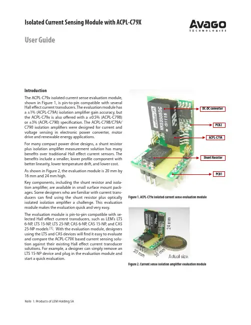
Isolated Current Sensing Module with ACPL-C79X User GuideIntroductionThe ACPL-C79x isolated current sense evaluation module, shown in Figure 1, is pin-to-pin compatible with several Hall effect current transducers. The evaluation module has a ±1% (ACPL-C79A) isolation amplifier gain accuracy, but the ACPL-C79x is also offered with a ±0.5% (ACPL-C79B) or ±3% (ACPL-C790) specification. The ACPL-C79B/C79A/ C790 isolation amplifiers were designed for current and voltage sensing in electronic power converter, motor drive and renewable energy applications.For many compact power drive designs, a shunt resistor plus isolation amplifier measurement solution has many benefits over traditional H all effect current sensors. The benefits include a smaller, lower profile component with better linearity, lower temperature drift, and lower cost. As shown in Figure 2, the evaluation module is 20 mm by 16 mm and 24 mm high.Key components, including the shunt resistor and isola-tion amplifier, are available in small surface mount pack-ages. Some designers who are familiar with current trans-ducers can find using the shunt resistor plus optically isolated isolation amplifier a challenge. This evaluation module makes the evaluation quick and very easy.The evaluation module is pin-to-pin compatible with se-lected H all effect current transducers, such as LEM’s LTS 6-NP, LTS 15-NP, LTS 25-NP, CAS 6-NP, CAS 15-NP, and CAS 25-NP models [1]. With the evaluation module, designers using the LTS and CAS devices will find it easy to evaluate and compare the ACPL-C79X based current sensing solu-tion against their existing H all effect current transducer solutions. For example, a designer can simply remove an LTS 15-NP device and plug in the evaluation module andstart a quick evaluation.Figure 1. ACPL-C79x isolated current sense evaluation moduleFigure 2. Current sense isolation amplifier evaluation moduleNote 1. Products of LEM Holding SAFor product information and a complete list of distributors, please go to our web site: Avago, Avago Technologies, and the A logo are trademarks of Avago Technologies in the United States and other countries.Data subject to change. Copyright © 2005-2012 Avago Technologies. All rights reserved. AV02-3742EN - August 7, 2012Figure 3. The Evaluation module schematicSchematicThe evaluation module circuit schematic is show in Figure 3. The evaluation module is made from two printed circuit boards (PCBs): PCB1 and PCB2. PCB1 has the shunt resis-tor and two header connectors to form a current path; a third header connector is used as an interface. PCB2 has an ACPL-C79A isolation amplifier (±1% gain accuracy) and an isolated DC-DC converter. The two PCBs are assembled with header connectors P4 and P5.AC or DC current through shunt resistor R1 results in a voltage that is proportional to current. This voltage is fil-tered by the anti-aliasing filter formed by R2, R3 and C1 and then sensed by the differential input ACPL-C79A. A differential output voltage that is proportional to the in-put voltage is created on the other side of the optical iso-lation barrier.Following the isolation amplifier, an OPA237 configured as a difference amplifier converts the differential signal to a single-ended output. This stage can be configured to further amplify the signal, if required, and form a low-pass filter to limit the bandwidth.In the evaluation module, the difference amplifier is de-signed for a gain of 1 with a low-pass filter corner frequen-cy of 234 kHz. Resistors R6 and R7 can be selected for a different gain. The bandwidth can be reduced by adding capacitors to the positions of C6 and C8.With the ACPL-C79A gain of 8.2, the overall transfer func-tion is:Vout = I × R1 × 8.2 + Vref .The output signal, Vout, is then connected to the next stage, such as a signal processor, through the P7 header connector, pin 3.Shunt Resistor and Current RangeThe shunt resistor in this module is fixed at 10 milliohm. The appropriate current measurement range is about 15 A RMS . This is calculated from the nominal input range of ±200 mV of the ACPL-C79A. The ACPL-C79x specifies a full scale input range of ±300 mV, which allows accurate overload current detection of up to 21 A PEAK . Because the evaluation module does not provide good heat dissipa-tion for the shunt resistor due to small PCB size, limit cur-rent to 10 A RMS during evaluation or for a quick functional check at 15 A RMS . For a detailed performance evaluation, a PCB with proper layout for the shunt resistor and other components is recommended.Power SuppliesThe evaluation module works on a single 5 V supply, which can be the same power supply for the signal pro-cessor and controller device connected through pin 1 and 2 of P7.The isolated DC-DC converter (U1 in Figure 3) is included in the evaluation module to power up the signal input side of the ACPL C79A; this makes the evaluation an easy plug-and-play operation. However, to make an ACPL C79A based solution cost effective in mass production, the 5 V supply would usually be supplied by a floating power sup-ply, which in many applications could be the same supply that is used to drive the high-side power transistor. A sim-ple three-terminal voltage regulator will provide a stable voltage. Another method is to add an additional winding to an existing transformer to produce a 5 V supply.Note *: Dotted lines denote header pin connections.。

DAT ASHEETNI 92374 AI, ±25 mV/V, 24 Bit, 50 kS/s/ch Simultaneous, Bridge Completion• 4 channels, 50 kS/s per channel simultaneous AI•±25 mV/V input range, 24-bit resolution•Programmable half- and full-bridge completionwith up to 10 V internal excitation•60 VDC, Category I bank isolation•RJ50 or D-SUB connectivity options•-40 °C to 70 °C operating range, 5 g vibration,50 g shockThe NI 9237 simultaneous bridge module for use with CompactDAQ and CompactRIO contains all the signal conditioning required to power and measure up to four bridge-based sensors simultaneously. The four RJ50 jacks provide direct connectivity to most torque or load cells and offer custom cable solutions with minimal tools. The high sampling rate and bandwidth of the NI 9237 offer a high-quality, high-speed strain or load measurement system with zero interchannel phase delay. With 60 VDC isolation and 1,000 Vrms transient isolation, the NI 9237 has high-common-mode noise rejection and increased safety for both the operator and test system.The NI 9237 can perform offset/null as well as shunt calibration and remote sense, making the module the best choice for strain and bridge measurements.The NI 9944 and NI 9945 are accessories for use with quarter-bridge sensors. These accessories have a female RJ50 connector on one end and screw terminals on the other end.C SERIES SIMULTANEOUS BRIDGE MODULE COMPARISONModel ChannelsSample Rate Resolution Connectivity Simultaneous Supported Bridges NI 9218NI 9219NI 9235NI 9236NI 923751.2 kS/s/ch 100 S/s/ch 10 kS/s/ch 10 kS/s/ch 50 kS/s/ch24 bits 24 bits 24 bits 24 bits 24 bitsQuarter, Half, Full Quarter, Half, Full 120 Ω Quarter Bridge 350 Ω Quarter Bridge Quarter, Half, FullLEMO,9-pin DSUB Spring Terminal Spring T erminal Spring T erminal RJ-50,DSUB24884NI C Series OverviewNI provides more than 100 C Series modules for measurement, control, and communication applications. C Series modules can connect to any sensor or bus and allow for high-accuracy measurements that meet the demands of advanced data acquisition and control applications.•Measurement-specific signal conditioning that connects to an array of sensors and signals •Isolation options such as bank-to-bank, channel-to-channel, and channel-to-earth ground •-40 °C to 70 °C temperature range to meet a variety of application and environmentalneeds •Hot-swappable The majority of C Series modules are supported in both CompactRIO and CompactDAQ platforms and you can move modules from one platform to the other with no modification.2 | | NI 9237 DatasheetCompactRIOCompactRIO combines an open-embedded architecturewith small size, extreme ruggedness, and C Seriesmodules in a platform powered by the NI LabVIEWreconfigurable I/O (RIO) architecture. Each systemcontains an FPGA for custom timing, triggering, andprocessing with a wide array of available modular I/O tomeet any embedded application requirement. CompactDAQCompactDAQ is a portable, rugged data acquisition platformthat integrates connectivity, data acquisition, and signalconditioning into modular I/O for directly interfacing to anysensor or signal. Using CompactDAQ with LabVIEW, youcan easily customize how you acquire, analyze, visualize,and manage your measurement data.SoftwareLabVIEW Professional Development System for Windows•Use advanced software tools for large project development•Generate code automatically using DAQ Assistant and InstrumentI/O Assistant•Use advanced measurement analysis and digital signal processing•Take advantage of open connectivity with DLLs, ActiveX,and .NET objects•Build DLLs, executables, and MSI installersNI LabVIEW FPGA Module•Design FPGA applications for NI RIO hardware•Program with the same graphical environment used for desktop andreal-time applications•Execute control algorithms with loop rates up to 300 MHz•Implement custom timing and triggering logic, digital protocols, andDSP algorithms•Incorporate existing HDL code and third-party IP including Xilinx IPgenerator functions•Purchase as part of the LabVIEW Embedded Control and MonitoringSuiteNI 9237 Datasheet| © National Instruments| 3NI LabVIEW Real-Time Module•Design deterministic real-time applications with LabVIEWgraphical programming•Download to dedicated NI or third-party hardware for reliableexecution and a wide selection of I/O•Take advantage of built-in PID control, signal processing, andanalysis functions•Automatically take advantage of multicore CPUs or setprocessor affinity manually•Take advantage of real-time OS, development and debuggingsupport, and board support•Purchase individually or as part of a LabVIEW suiteCircuitryEach channel on the NI 9237 has an independent 24-bit ADC and an input amplifier that enable you to sample signals from all four channels simultaneously.The NI 9237 is isolated from earth ground. However, the individual channels are not isolated from each other. The EX+, EX-, and T- signals are common among all channels. You can connect the NI 9237 to a device that is biased at any voltage within the NI 9237 rejection range of earth ground.Figure 1. Input Circuitry for One Channel of the NI 9237Connection Options to Correct for Resistance Errors Wiring resistance can create errors in bridge circuits. The NI 9237 provides two mechanisms to correct for these errors: remote sensing and shunt calibration.Remote SensingRemote sensing continuously and automatically corrects for errors in excitation leads, and generally is most appropriate for half- and full-bridge sensors.Long wire and small gauge wire have greater resistance, which can result in gain error. The resistance in the wires that connect the excitation voltage to the bridge causes a voltage drop, 4| | NI 9237 Datasheetwhich is a source of gain error. The NI 9237 includes remote sensing to compensate for this gain error. Connect remote sense wires to the points where the excitation voltage wires connect to the bridge circuit. Refer to the following figure for an illustration of how to connect remote sense wires to the NI 9237.Figure 2. Connecting Remote Sense Wires to the NI 9237RRThe actual bridge excitation voltage is smaller than the voltage at the EX+ and EX- leads. If you do not use remote sensing of the actual bridge voltage, the resulting gain error is:BB BBB for half‐bridge sensors and2⋅BBBBB for full‐bridge sensors.If you connect the remote sense signals directly to the bridge resistors, the NI 9237 senses the actual bridge voltage and eliminates the gain errors caused by the resistance of the EX+ and EX- leads.Shunt CalibrationShunt calibration can correct for errors from the resistance of both the excitation wiring and wiring in the individual resistors of the bridge. Remote sensing corrects for resistances from the EX pins on the NI 9237 to the sensor, and shunt calibration corrects for these errors and for errors caused by wire resistance within an arm of the bridge. Shunt calibration is most useful with quarter-bridge sensors because there may be significant resistance in the wiring to the active resistor in the bridge.The NI 9237 shunt calibration circuitry consists of a precision resistor and a software-controlled switch. Refer to the software help for information about enabling the shunt calibration switch for the NI 9237.Shunt calibration involves simulating the input of strain by changing the resistance of an arm in the bridge by some known amount. This is accomplished by shunting, or connecting, a large resistor of known value across one arm of the bridge, creating a known strain-induced change in resistance. You can then measure the output of the bridge and compare it to the expected voltage value. You can use the results to correct gain errors in the entire measurement path, or to simply verify general operation to gain confidence in the setup.NI 9237 Datasheet| © National Instruments| 5Use a stable signal, which is typically the unloaded state of the sensor, first with the shunt calibration switch off and then again with the switch on. The difference in these two measurements provides an indication of the gain errors from wiring resistances. You can design the software application to correct subsequent readings for this gain error.Excitation VoltagesYou can program the NI 9237 to supply 2.5 V , 3.3 V , 5 V , or 10 V of excitation voltage. Themaximum excitation power for internal excitation is 150 mW.Note Unless you supply external excitation voltage, NI recommends that you setthe excitation voltage to a value that keeps the total power below 150 mW. The NI 9237 automatically reduces internal excitation voltages as needed to stay below 150 mW total power.Use the following equation to calculate the power of a single bridge:=B 2where R is the total resistance of the bridge.For a quarter or half bridge, R is equal to two times the resistance of each element. For a full bridge, R is equal to the resistance of each element.The 150 mW limit allows you to power half and full bridges as follows:•Four 350 Ω half bridges at 5.0 V •Four 350 Ω full bridges at 3.3 V •Four 120 Ω half bridges at 2.5 VExternal ExcitationYou can connect an external excitation voltage source to the NI 9237 if you need an excitation voltage that causes more than 150 mW to dissipate across all the bridges.Figure 3. Connecting an External Excitation Voltage Source to the NI 9237External Excitation VoltageSourceExternal Excitation Voltage SourceNote For the NI 9237 with RJ-50, use the two EX+ and EX- terminals on the four-terminal external excitation voltage connector to connect one external excitation source.You can use the additional EX+ and EX- terminals on the connector to wire multiple NI 9237modules together in a daisy chain.6 | | NI 9237 DatasheetFilteringThe NI 9237 uses a combination of analog and digital filtering to provide an accurate representation of in-band signals and reject out-of-band signals. The filters discriminatebetween signals based on the frequency range, or bandwidth, of the signal. The three important bandwidths to consider are the passband, the stopband, and the anti-imaging bandwidth.The NI 9237 represents signals within the passband, as quantified primarily by passband ripple and phase nonlinearity. All signals that appear in the alias-free bandwidth are either unaliased signals or signals that have been filtered by at least the amount of the stopband rejection.PassbandThe signals within the passband have frequency-dependent gain or attenuation. The small amount of variation in gain with respect to frequency is called the passband flatness. Thedigital filters of the NI 9237 adjust the frequency range of the passband to match the data rate.Therefore, the amount of gain or attenuation at a given frequency depends on the data rate.Figure 4. Typical Passband Flatness for the NI 9237Frequency/Data Rate0.50.40.0250.000–0.025–0.0500.30.20.10G a i n (d B)StopbandThe filter significantly attenuates all signals above the stopband frequency. The primary goal of the filter is to prevent aliasing. Therefore, the stopband frequency scales precisely with the data rate. The stopband rejection is the minimum amount of attenuation applied by the filter to all signals with frequencies within the stopband.Alias-Free BandwidthAny signals that appear in the alias-free bandwidth are not aliased artifacts of signals at a higher frequency. The alias-free bandwidth is defined by the ability of the filter to reject frequencies above the stopband frequency. The alias-free bandwidth is equal to the data rate minus the stopband frequency.NI 9237 Datasheet | © National Instruments | 7Data RatesThe frequency of a master timebase (f M) controls the data rate (f s) of the NI 9237. The NI 9237 includes an internal master timebase with a frequency of 12.8 MHz, but the module also can accept an external master timebase or export its own master timebase. To synchronize the data rate of an NI 9237 with other modules that use master timebases to control sampling, all of the modules must share a single master timebase source.The following equation provides the available data rates of the NI 9237:=÷256where n is any integer from 1 to 31.However, the data rate must remain within the appropriate data rate range. When using the internal master timebase of 12.8 MHz, the result is data rates of 50 kS/s, 25 kS/s, 16.667 kS/s, and so on down to 1.613 kS/s depending on the value of n. When using an external timebase with a frequency other than 12.8 MHz, the NI 9237 has a different set of data rates.Note The NI 9151 R Series Expansion chassis does not support sharing timebasesbetween modules.NI 9237 SpecificationsThe following specifications are typical for the range -40 °C to 70 °C unless otherwise noted.Caution Do not operate the NI 9237 in a manner not specified in this document.Product misuse can result in a hazard. You can compromise the safety protectionbuilt into the product if the product is damaged in any way. If the product isdamaged, return it to NI for repair.Input CharacteristicsNumber of channels 4 analog input channelsBridge completionHalf and Full InternalQuarter ExternalADC resolution24 bitsType of ADC Delta-Sigma (with analog prefiltering) Sampling mode Simultaneous8| | NI 9237 DatasheetInternal master timebase (ƒM)Frequency12.8 MHzAccuracy±100 ppm maximumData rate range (ƒs) using internal master timebaseMinimum 1.613 kS/sMaximum50 kS/sData rate range (ƒs) using external master timebaseMinimum391 S/sMaximum51.36 kS/sData rates (ƒs)(ƒM ÷ 256) ÷ n, where n = 1, 2, …, 31 Typical input range±25 mV/VScaling coefficient 2.9802 nV/V per LSBOvervoltage protection between any two pins±30 VGain drift10 ppm/°C maximumOffset drift2.5 V excitation0.6 µV/V per °C3.3 V excitation0.5 µV/V per °C5 V excitation0.3 µV/V per °C10 V excitation0.2 µV/V per °C1Before offset null or shunt calibration.2Applies at a data rate of 50 kS/s. Lower data rates can have up to 0.20% of reading additional gain error.3Range equals 25 mV/V.4Uncalibrated accuracy refers to the accuracy achieved when acquiring data in raw or unscaledmodes and in which calibration constants that are stored in the module are not applied to the data.NI 9237 Datasheet| © National Instruments| 9Half-bridge completionTolerance±1200 µV/V maximumDrift 1.5 µV/V per °CTable 2. Channel-to-Channel Matching (Calibrated)Phase nonlinearityƒin = 0 to 1 kHz<0.001°ƒin = 0 to 20 kHz±0.1°Input delay(40 + 5/512)/ƒs + 4.5 µs PassbandFrequency0.45 · ƒsFlatness0.1 dB maximum StopbandFrequency0.55 · ƒsRejection100 dBAlias-free bandwidth0.45 · ƒsOversample rate64 · ƒsRejection at oversample rate5ƒs = 10 kS/s60 dB @ 640 kHzƒs = 50 kS/s*********** Common-mode voltage,all signals to earth ground±60 VDCCommon-mode voltage range, with respect to EX-±1 V from the midpoint of the excitation voltage5Rejection by analog prefilter of signal frequencies at oversample rate. 10| | NI 9237 DatasheetCMRRRelative to earth ground6 (ƒin = 0 to 60140 dBHz)Relative to EX– (ƒin = 0 to 1 kHz)85 dBSFDR (1 kHz, –60 dBFS)115 dBTotal Harmonic Distortion (THD)1 kHz, –20 dBFS–95 dB8 kHz, –20 dBFS–95 dBExcitation noise100 µVrmsCrosstalk (not including cable effects)ƒin = 1 kHz110 dBƒin = 10 kHz100 dBExcitationInternal voltage 2.5 V, 3.3 V, 5.0 V, 10.0 VInternal power150 mW maximumExternal voltage 2 V to 10 VShunt calibrationResistance100 kΩ6Measured with a balanced cable on the NI 9237 with RJ-50 and with no cable on theNI 9237 with DSUB. Shielded cables that are not twisted-pair may be significantly unbalanced, which can impact CMRR performance. To improve the balance of shielded cables, NI recommends twisting together the AI+/AI– pair, the RS+/RS– pair, and the EX+/EX– pair.NI 9237 Datasheet| © National Instruments| 11Resistor accuracy25 °C±110 Ω– 40 °C to 70 °C±200 ΩMTBFNI 9237 with RJ-50603,359 hours at 25 °C; Bellcore Issue 2,Method 1, Case 3, Limited Part Stress Method NI 9237 with DSUB704,148 hours at 25 °C; Bellcore Issue 2,Method 1, Case 3, Limited Part Stress Method Power RequirementsPower consumption from chassisActive mode740 mW maximumSleep mode25 µW maximumThermal dissipation (at 70 °C)Active mode740 mW maximumSleep mode25 µW maximumPhysical CharacteristicsTip For two-dimensional drawings and three-dimensional models of the C Seriesmodule and connectors, visit /dimensions and search by module number.Connect only voltages that are within the following limits.Between any two pins±30 V maximumIsolation, channel-to-channel NoneIsolation, channel-to-earth groundUp to 3,000 mContinuous60 VDC, Measurement Category IWithstand1,000 Vrms, verified by a 5 s dielectricwithstand testUp to 5,000 mContinuous60 VDC, Measurement Category IWithstand860 Vrms, verified by a 5 s dielectricwithstand test12| | NI 9237 DatasheetMeasurement Category I is for measurements performed on circuits not directly connected to the electrical distribution system referred to as MAINS voltage. MAINS is a hazardous live electrical supply system that powers equipment. This category is for measurements of voltages from specially protected secondary circuits. Such voltage measurements include signal levels, special equipment, limited-energy parts of equipment, circuits powered by regulated low-voltage sources, and electronics.Caution Do not connect the NI 9237 to signals or use for measurements withinMeasurement Categories II, III, or IV.Note Measurement Categories CAT I and CAT O are equivalent. These test andmeasurement circuits are not intended for direct connection to the MAINS buildinginstallations of Measurement Categories CAT II, CAT III, or CAT IV. Hazardous LocationsU.S. (UL)Class I, Division 2, Groups A, B, C, D, T4;Class I, Zone 2, AEx nA IIC T4Canada (C-UL)Class I, Division 2, Groups A, B, C, D, T4;Class I, Zone 2, Ex nA IIC T4Europe (ATEX) and International (IECEx)Ex nA IIC T4 GcSafety and Hazardous Locations StandardsThis product is designed to meet the requirements of the following electrical equipment safety standards for measurement, control, and laboratory use:•IEC 61010-1, EN 61010-1•UL 61010-1, CSA 61010-1•EN 60079-0:2012, EN 60079-15:2010•IEC 60079-0: Ed 6, IEC 60079-15; Ed 4•UL 60079-0; Ed 5, UL 60079-15; Ed 3•CSA 60079-0:2011, CSA 60079-15:2012Note For UL and other safety certifications, refer to the product label or the OnlineProduct Certification section.Electromagnetic CompatibilityThis product meets the requirements of the following EMC standards for sensitive electrical equipment for measurement, control, and laboratory use:•EN 61326-2-1 (IEC 61326-2-1): Class A emissions; Industrial immunity•EN 55011 (CISPR 11): Group 1, Class A emissions•AS/NZS CISPR 11: Group 1, Class A emissionsNI 9237 Datasheet| © National Instruments| 13•FCC 47 CFR Part 15B: Class A emissions•ICES-001: Class A emissionsNote In the United States (per FCC 47 CFR), Class A equipment is intended foruse in commercial, light-industrial, and heavy-industrial locations. In Europe,Canada, Australia and New Zealand (per CISPR 11) Class A equipment is intendedfor use only in heavy-industrial locations.Note Group 1 equipment (per CISPR 11) is any industrial, scientific, or medicalequipment that does not intentionally generate radio frequency energy for thetreatment of material or inspection/analysis purposes.Note For EMC declarations and certifications, and additional information, refer tothe Online Product Certification section.CE ComplianceThis product meets the essential requirements of applicable European Directives, as follows:•2014/35/EU; Low-V oltage Directive (safety)•2014/30/EU; Electromagnetic Compatibility Directive (EMC)•94/9/EC; Potentially Explosive Atmospheres (ATEX)Online Product CertificationRefer to the product Declaration of Conformity (DoC) for additional regulatory compliance information. To obtain product certifications and the DoC for this product, visit / certification, search by model number or product line, and click the appropriate link in the Certification column.Shock and VibrationTo meet these specifications, you must panel mount the system.Operating vibrationRandom (IEC 60068-2-64) 5 g rms, 10 Hz to 500 HzSinusoidal (IEC 60068-2-6) 5 g, 10 Hz to 500 HzOperating shock (IEC 60068-2-27)30 g, 11 ms half sine; 50 g, 3 ms half sine;18 shocks at 6 orientations14| | NI 9237 DatasheetEnvironmentalRefer to the manual for the chassis you are using for more information about meeting these specifications.Operating temperature-40 °C to 70 °C(IEC 60068-2-1, IEC 60068-2-2)-40 °C to 85 °CStorage temperature(IEC 60068-2-1, IEC 60068-2-2)Ingress ProtectionNI 9237 with RJ-50IP30NI 9237 with DSUB IP40Operating humidity (IEC 60068-2-78)10% RH to 90% RH, noncondensing Storage humidity (IEC 60068-2-78)5% RH to 95% RH, noncondensing Pollution Degree2Maximum altitude5,000 mIndoor use only.Environmental ManagementNI is committed to designing and manufacturing products in an environmentally responsible manner. NI recognizes that eliminating certain hazardous substances from our products is beneficial to the environment and to NI customers.For additional environmental information, refer to the Minimize Our Environmental Impact web page at /environment. This page contains the environmental regulations and directives with which NI complies, as well as other environmental information not included in this document.Waste Electrical and Electronic Equipment (WEEE) EU Customers At the end of the product life cycle, all NI products must bedisposed of according to local laws and regulations. For more information abouthow to recycle NI products in your region, visit /environment/weee.电子信息产品污染控制管理办法(中国RoHS)中国客户National Instruments符合中国电子信息产品中限制使用某些有害物质指令(RoHS)。

General DescriptionThe MAX1702 evaluation kit (EV kit) is a fully assembled and tested surface-mount circuit board that demonstrates the M AX1702B power-management IC. The IC is opti-mized for microprocessor-based applications. The MAX1702B integrates three high-performance step-down DC-DC power supplies with associated supervisory and management functions. The first power supply (VI/O) is configured for 3.3V and provides up to 900mA. The sec-ond power supply (VCORE) is configured for 1.1V and provides up to 400mA. The third power supply (VM EM )can be configured to 1.8V, 2.5V, or 3.3V and provides up to 800mA. Power management functions include auto-matic power-up sequencing, power-on reset, manual reset with timer, and two levels of low-battery detection. The EV kit operates with a 2.6V to 5.5V input voltage range, allowing the use of batteries or a regulated DC power supply at the input.Featureso Triple-Output Power Supply3.3V VI/O Peripheral Output 1.1V VCORE µP Core Output1.8V,2.5V, or3.3V Selectable VMEM Memory Outputo Internal Switcheso 1MHz Pulse-Width Modulation (PWM) Switching o Adjustable Dead/Low-Battery Settings o 900mA Available from the VI/O Output o 800mA Available from the VMEM Output o 400mA Available from the VCORE Output o Surface-Mount Construction o Fully Assembled and TestedEvaluates: MAX1702BMAX1702 Evaluation Kit19-2517; Rev. 0; 7/02Ordering InformationFor pricing, delivery, and ordering information,please contact Maxim/Dallas Direct!at 1-888-629-4642, or visit Maxim’s website at .E v a l u a t e s : M A X 1702BMAX1702 Evaluation Kit 2_______________________________________________________________________________________Quick StartThe M AX1702 EV kit is a fully assembled and tested surface-mount board. Follow the steps below for board operation. Do not turn on the power supply until all connections are completed:1)Verify that a shunt is across pins 1 and 2 of jumper JU1 (ON2).2)Verify that a shunt is across pins 1 and 3 of jumper JU3 (PGM3).3)Connect a voltmeter across the VI/O pad and IGND pad to monitor the VI/O output voltage.4)Connect a voltmeter across the VCORE pad and CGND pad to monitor the VCORE output voltage.5)Connect a voltmeter across the VM EM pad and MGND pad to monitor the VMEM output voltage.6)Connect the positive terminal of a 4.5V supply to the VIN pad. Connect the negative terminal to the GND pad.7)Turn on the power supply and verify that the VI/O output is at 3.3V, VCORE output is at 1.1V, and VMEM output is at 2.5V.8)Use a voltmeter to verify that LBO , OUTOK, and RSO are at 3.3V and REF is at 1.25V.Detailed DescriptionThe M AX1702 EV kit is a fully assembled and tested surface-mount circuit board that demonstrates the capability of the M AX1702B triple-output step-down DC-DC converter optimized for microprocessor-based applications. The MAX1702B integrates three high-per-formance, 1M Hz PWM switching, step-down DC-DC power supplies. These power supplies can be used to power the microprocessor, memory, and I/O peripher-als in a single system. The microprocessor VCORE supply is configured for 1.1V and provides up to 400mA. The memory VM EM supply is configurable to 1.8V, 2.5V, or 3.3V and provides up to 800mA. The I/O peripheral VI/O supply is configured for 3.3V and pro-vides up to 900mA. The VPLL output is a filtered output from VCORE that can be used to supply noise-sensitive circuitry such as a phase-lock loop.The EV kit input voltage range is 2.6V to 5.5V and requires up to 2A of current from the source with all outputs fully loaded.Input SourceThe M AX1702 EV kit has a 2.6V to 5.5V input voltage range that allows the use of batteries or a regulated DC power supply as the power source. However, the EV kit requires a minimum of 3.6V at the input for the VI/O out-put supply to regulate to 3.3V ±2%. If the input voltage falls below 3.6V, VI/O tracks the input voltage. If VMEM is configured to regulate at 3.3V, it also tracks the input voltage below 3.6V.Input ThresholdsThe M AX1702B contains two low-battery detection thresholds, dead battery (DBI) and low-battery (LBI),that are used to monitor the input power source to the EV kit. These thresholds are programmable with exter-nal resistors. The DBI threshold is set to 2.7V and theR3. If the input source falls below the LBI threshold, the low-battery LBO output is pulled low. The EV kit enters shutdown mode when the input source falls below the DBI threshold. Replace resistors R1, R2, and R3 with different values to reconfigure the DBI and LBI thresh-olds. Refer to the MAX1702B data sheet to select new resistor values for R1, R2, and R3.Power-Up SequenceThe M AX1702 EV kit power-up sequence is initiated when the input voltage is greater than the dead-battery setting (DBI) and greater than the UVLO threshold (2.4V). During initial power-up, VI/O first ramps up in a soft-start mode. Once VI/O reaches its regulation volt-age, VM EM ramps to its target in soft-start mode.Finally, once VM EM reaches its regulation voltage,VCORE ramps to its target in soft-start mode. The reset output RSO is held low during this time. Once the VCORE output has reached its target voltage, a 65.5ms reset timer is started. RSO is pulled high when the timer expires. The timer may be manually reset by pushing the momentary switch SW1 or by applying a logic-low signal at the MR pad. The outputs stay on during the manual reset.Triple OutputsThe M AX1702 EV kit features three (VCORE, VM EM ,and VI/O) step-down DC-DC converters that can be setto regulate to different voltages. VCORE can supply 400mA at an output voltage of 1.1V. The VCORE output voltage is set with resistors R5 and R6. Refer to the Setting the Output Voltages section in the M AX1702Bdata sheet for instructions on selecting resistors R5 and R6. VM EM can supply 800mA at an output voltage of 3.3V, 2.5V, or 1.8V and can be set by configuring JU2.See Table 1 for JU2 configuration. VI/O output voltage is fixed to 3.3V and can supply 900mA.SLEEP ModeThe EV kit contains a 3-pin jumper (JU1) that can be used to enable the M AX1702B in normal mode or to place it in sleep mode. In normal operation, the three converters are enabled. In sleep mode, VCORE is in shutdown while VI/O and VMEM remain enabled. Sleep mode allows the microprocessor to enter sleep mode while memory and I/O peripherals are kept alive in a system application. See Table 2 for JU1 configuration.Normal and sleep modes can also be controlled with an external device by removing the shunt on JU1 and applying a CMOS logic-level signal to the ON2 pad.OUTOK OutputThe M AX1702 EV kit provides an OUTOK logic output signal to indicate the regulation state of VCORE. A logic low at the OUTOK pad indicates that the VCORE output has dropped to 92.5% of its regulation voltage. A logic high at OUTOK indicates that VCORE is 95.5% of its regulation voltage.Evaluates: MAX1702BMAX1702 Evaluation Kit_______________________________________________________________________________________3Table 1. VMEM Output Settings (JU2)E v a l u a t e s : M A X 1702BMAX1702 Evaluation Kit 4_______________________________________________________________________________________Figure 1. MAX1702 EV Kit SchematicMAX1702 Evaluation KitEvaluates: MAX1702BMaxim c annot assume responsibility for use of any c irc uitry other than c irc uitry entirely embodied in a Maxim produc t. No c irc uit patent lic enses are implied. Maxim reserves the right to change the circuitry and specifications without notice at any time.Maxim Integrated Products, 120 San Gabriel Drive, Sunnyvale, CA 94086 408-737-7600____________________5©2002 Maxim Integrated ProductsPrinted USAis a registered trademark of Maxim Integrated Products.Figure 2. MAX1702 EV Kit Component Placement Guide—Component SideFigure 3. MAX1702 EV Kit PC Board Layout—Component SideFigure 4. MAX1702 EV Kit PC Layout—Solder Side。

© 2009 Microchip Technology Inc.DS01299A-page 1AN1299INTRODUCTIONA large number of motor control applications are consistently and continuously looking for methods to improve efficiency while reducing system cost. These are the two main factors that are driving the efforts to improve existing motor control techniques, such as trapezoidal control, scalar control and Field-Oriented Control (FOC).FOC has become more popular in recent years due to the fact that the cost required to implement this technique is no longer a constraint. The available technology and manufacturing process now make it possible to implement this control technique in a 16-bit fixed-point machine such as the dsPIC ® Digital Signal Controller (DSC).Efficiency is another reason that has allowed FOC to gain ground over scalar and trapezoidal control techniques on low-cost and mid-cost applications. It is also well suited in applications in which hard requirements are low noise, low torque ripple and good torque control over a vast speed range.Field-oriented control can be implemented using position sensors such as encoders, resolvers or Hall sensors. However, not all motor control applications require such granularity given by a resolver or encoder;and, in many cases, they do not require control at zero speed.These applications are a perfect target for using sensorless techniques in which the motor position can be estimated using the information provided by the currents flowing through the motor coils. There are two popular approaches to this sensing technique: the dual-shunt resistor and the single-shunt resistor.The dual-shunt resistor technique utilizes the information contained in the current flowing through two motor coils in order to estimate the motor position.The single-shunt resistor technique utilizes only the information contained in the current flowing through the DC bus to reconstruct the three-phase currents, and then estimate motor position.In this application note, the single-shunt approach is discussed. For information on the dual-shunt resistor approach, please refer to the application note, AN1078“Sensorless Field Oriented Control of PMSM Motors”.CURRENT MEASUREMENTThe information contained in the current flowing through the motor coils allows a motor control algorithm to operate the motor in a region where the motor produces the maximum torque, or to operate the motor at certain performance, or even to be able to approximate or estimate internal motor variables such as position.Three-phase AC Induction Motors (ACIMs),Permanent Magnet Synchronous Motors (PMSMs) and Brushless Direct Current (BLDC) motors in particular use a three-phase inverter as the topology of preference. This topology, which is shown in Figure 1,allows individual control of the energy applied to each coil, which enables the motor to be efficiently operated.FIGURE 1:THREE-PHASE INVERTER TOPOLOGYAuthors:Daniel Torres and Jorge Zambada Microchip Technology Inc.3-Phase InverterRectifierDC BusThree-Phase ACMotorSingle-Shunt Three-Phase Current ReconstructionAlgorithm for Sensorless FOC of a PMSMAN1299DS01299A-page 2© 2009 Microchip Technology Inc.The three-phase inverter is compounded by three legs.Each leg contains two electronic switches that are arranged in such a way that create a half-bridge topology. Therefore, current can flow in both directions to and from the legs. The electronic switches can be either power MOSFETs or IGBTs.Current MOSFET and IGBT manufacturing technologies have allowed digital controllers to take advantage of Pulse-Width Modulation (PWM)techniques to control the amount of energy applied to each coil.The most common techniques used are sinusoidal modulation, third-harmonic modulation and Space Vector Modulation (SVM). These PWM techniques are suitable to operate the electronic switches in saturation mode, which helps to increase system efficiency. In order to determine the amount of current flowing through the coils, a shunt resistor is required on each coil. A typical three-phase inverter with current measurement on three phases is shown in Figure 2.FIGURE 2:CIRCUIT FOR MEASURING CURRENT IN THREEAssuming there is a balanced load, we can consider that the sum of the three phases is equal to zero, as described by Kirchhoff’s Current Law. This law is shown in Equation 1.EQUATION 1:KIRCHHOFF’S CURRENT LAWTherefore, by measuring only two, the third can be solved using Equation 1. A simplified version using two shunt resistors is shown in Figure 3.FIGURE 3:CIRCUIT FOR MEASURING CURRENT IN TWO PHASESThe intention of the algorithm presented in this application note is to be able to measure all three phases with a single-shunt resistor and a single differential amplifier. A circuit showing a single-shunt resistor is shown in Figure 4.FIGURE 4:CIRCUIT FOR MEASURING CURRENT FLOWING THROUGH DC BUSI A + I B + I C = 0V BUS3 ~I B I AI C = -I B -I AV BUS3 ~I BUSAN1299ADVANTAGES AND DISADVANTAGES OF USING A SINGLE-SHUNT RESISTOR AdvantagesAs previously mentioned, one of most important reasons for single-shunt three-phase reconstruction is cost reduction. Which in turn, simplifies the sampling circuit to one shunt resistor and one differential amplifier.In addition to cost reduction benefits, the single-shunt algorithm allows the use of power modules that do not provide individual ground connection of each phase. Another benefit of single-shunt measurement is that the same circuit is being used to sense all three phases. Gains and offset will be the same for all measurements, which eliminates the need to calibrate each phase amplification circuit or compensate in software.DisadvantagesDuring single-shunt measurements, a modification on the sinusoidal-modulation pattern needs to be made in order to allow current to be measured. This pattern modification could generate some current ripple. Due to modification of patterns and correction of the same modifications, more CPU is used to implement this algorithm.IMPLEMENTATION DETAILSIn order to drive the motor with AC signals, PWM methods are used to drive the switching transistors shown in the three-phase inverter. This modulation and resulting modulated waveform are shown in Figure5.A sinusoidal waveform can be generated by loading a series of duty cycle values into the PWM generator module. The values in the lookup table represent a modulated sine wave, so once these duty cycles are fed into the motor windings through the inverter, the motor windings will filter the switching pattern. The resulting sine wave is shown Figure5.The downside of a lookup table with sine values is the maximum value that can be achieved. This value is limited to 86% of the input voltage. Another sinusoidal modulation method is Space Vector Modulation, which is used to overcome this limitation. SVM allows 100% utilization of input voltage. SVM is described and used in several application notes such as AN908 “Using the dsPIC30F for Vector Control of an ACIM” and AN1017“Sinusoidal Control of PMSM Motors with dsPIC30F DSC”. The typical voltage shape generated using SVM is shown in Figure6.FIGURE 5:SINUSOIDAL MODULATION© 2009 Microchip Technology Inc.DS01299A-page 3AN1299DS01299A-page 4© 2009 Microchip Technology Inc.FIGURE 6:SPACE VECTOR MODULATION (SVM)When calculating the resulting voltage from line-to-line,we get three sinusoidal waveforms phase shifted 120°,as shown in Figure 7.FIGURE 7:CALCULATED LINE-TO-LINE VOLTAGEPWM1PWM2PWM3100%50%0%II I III IV V VISVM SectorV A -V B V B -V C V C -V A+V BUS0V-V BUS II I III IV V VISVM SectorAN1299SVM and Current Measurement RelationshipWhen measuring current through a single-shunt resistor, the state of the bottom switches is critical. To show this, Sector I of SVM is magnified in Figure8. In addition, PWM waveforms on each switching transistor are also shown.To observe the relationship between PWM modulation and current measurement through a single-shunt resistor, let us consider PWM Cycle 2 as an example. Since we are only interested in the low-side switch PWM, we will only show the PWMxL components of the PWM (Figure9).© 2009 Microchip Technology Inc.DS01299A-page 5AN1299DS01299A-page 6© 2009 Microchip Technology Inc.Looking at the three-phase inverter, we will analyze all of the different PWMxL combinations (T0, T1, T2 and T3) for this period to see what the current measurement represents. Starting with T0, we have the following combination of the electronic switches (MOSFETs or IGBTs) in the inverter, where we see that there is no current flowing through the single-shunt resistor (Figure 10).FIGURE 10:NO CURRENT FLOWING THROUGH THE SHUNTMoving on to T1, we see that PWM2L is active, while PWM1H and PWM3H are active as well (not currently shown, but assuming PWM outputs are complementary). Since there is current flowing into the motor through phases A and C, and coming out of phase B, we can consider this current measurement to represent –I B , as shown in Figure 11.FIGURE 11:CURRENT I B FLOWING THROUGH THE SHUNT RESISTORDuring T2, PWM2L and PWM3L are active, and PWM1H is active. This combination gives us current I A flowing through the single-shunt as shown in Figure 12.FIGURE 12:CURRENT I A FLOWING THROUGH THE SHUNT RESISTORT3 is the same scenario as T0, where there is no current flowing through the shunt resistor; therefore,I BUS = 0 as shown in Figure 13.FIGURE 13:NO CURRENT FLOWING THROUGH THE SHUNTThe pattern repeats the second half of the PWM period.Looking at a complete PWM cycle, there are two windows of time where current represents an actual phase current. In this example –I B and I A were measured in one PWM cycle. Since this is a balanced system, I C can be calculated using Equation 2. This allows three current measurements to be done in one PWM cycle using a single-shunt resistor.EQUATION 2:I C CALCULATIONA truth table (Table 1) was created to help illustrate what the measured current represents for all possible combinations of the electronic switches. First, let us name each electronic switch as shown in Figure 14.V BUS3 ~I BUS = -I BV BUS3 ~I BUS = I AI C = -I B -I A© 2009 Microchip Technology Inc.DS01299A-page 7AN1299FIGURE 14:SHUNT RESISTOR TRUTH TABLE NAMINGTable 1 shows what I BUS represents for all eight possible combinations of the circuit. Keep in mind that the H and L switches from the same leg cannot be ON at the same time to avoid shoot-through, so these combinations are not listed in the table. Also, any other combination that does not allow any current flowing through the shunt resistor is not listed in Table 1.TABLE 1:SHUNT RESISTOR TRUTH TABLESpecial CasesThere are special situations that do not allow single-shunt three-phase reconstruction.DUTY CYCLES ARE SIMILAR OR EQUAL DURING HIGH-MODULATION INDEXAs sinusoidal waveforms are generated with SVM,there are some PWM periods in which time windows where current is sampled, are simply not wide enough.One example of this situation is PWM cycle 1, which is shown in Figure 8. If we zoom in, we notice that PWM1L and PWM3L are the same, which leads to a T2of ‘0’. Figure 15 shows a magnification of this condition.This situation does not allow the controller to measure a second current. Therefore, three-phase current information cannot be constructed for that particular cycle.FIGURE 15:SAMPLING TIME WINDOW FOR SIMILAR DUTY CYCLESIH 2H 3H 1L 2L 3L I BUS ON OFF OFF OFF ON ON +I A OFF ON OFF ON OFF ON +I B OFF OFF ON ON ON OFF +I C OFF ON ON ON OFF OFF –I A ON OFF ON OFF ON OFF –I B ONONOFFOFFOFFON–I CT0T1T3T1T0T2 = 0PWM1L PWM2L PWM3LAN1299DS01299A-page 8© 2009 Microchip Technology Inc.DUTY CYCLE SIMILARITY DURING LOW-MODULATION INDEXLow-modulation index means that the amplitude of the modulating signal is low, as opposed to a high-modulation index where the duty cycle can go all the way to 100% due to a high-amplitude of the modulating signal. Low-modulation index is usually done when there is no load on the motor shaft. Therefore, the amplitude of the modulating signal is low. Since Complementary mode is used to modulate sinusoidal voltages, duty cycles are centered in 50% duty cycle. If we take the same sector as before, but for a low-modulation index, we will end up with a situation similar to what is shown in Figure 16.We can see how close the duty cycles are to 50% duty cycle. In fact, a modulation index of ‘0’ would be generating by 50%, duty cycles on all PWM outputs.Let us take a closer look at PWM cycle 4 to see what the limitation is when using a single-shunt resistor to reconstruct the three phases as shown in Figure 17.The two windows used to measure current through single-shunt, T1 and T2, may be too narrow to let the differential amplifier stabilize its output to a steady state value.FIGURE 17:SAMPLING TIME WINDOW FOR SIMILAR DUTY CYCLES DURING LOW-© 2009 Microchip Technology Inc.DS01299A-page 9AN1299DEAD TIMEAdditionally, dead time is also present during Complementary mode, reducing these time windows even further. Showing the same PWM cycle with high side outputs and dead time, we end up with a situation similar to what is shown Figure 18.FIGURE 18:SAMPLING TIME WINDOW AFFECTED BY DEAD TIMEDead time also affects the time window where single-shunt current measurements are done. The minimum time window to measure current through single-shunt depends on the following parameters:•PWM Frequency:This is because the higher the PWM frequency is,the smaller all of these time window values are.•Dead Time Required by the System:As shown in the previous figure, dead time directly affects the measurement window.•Hardware:Differential amplifier slew rate, output filter delay and MOSFET switching noise affect this measure-ment window as well.HARDWAREIn order to illustrate how the hardware affects the single-shunt measurement, let us take a closer look at the first half of the period of the last PWM cycle (Figure 18) to see what the output of the actual single-shunt conditioning circuitry (shown in Figure 19) looks like.FIGURE 19:HARDWARE UTILIZED FOR MEASURING CURRENT USING A SINGLE-SHUNT RESISTORThe effective measurement window is reduced to whenever the output of the amplifier is stable, which means after MOSFET switching noise, dead time, the operation amplifier’s slew rate, and the output RC filter settling time. These effects are shown in Figure 20.PWM1HPWM1L PWM2H PWM2L PWM3H PWM3LT0T1T2T3T2T1T0+-AV DD AV DD /2I B U SI BUS SenseAN1299DS01299A-page 10© 2009 Microchip Technology Inc.FIGURE 20:HARDWARE EFFECTS ON SAMPLING TIME WINDOWZooming in to the transient response of the amplifier (shown in Figure 21), the green box shows where it is okay to sample at T1. However, since T2 is not wide enough, current cannot be sampled during T2. The transient response in gray represents the time to sample T2 if it would have been wide enough.FIGURE 21:MAGNIFICATION OF THE HARDWARE EFFECTS ON THE SAMPLING TIME WINDOWIn general, single-shunt reconstruction of three-phase currents is not possible when modulating the shaded areas from the hexagon shown in Figure 22.FIGURE 22:CRITICAL SVM VECTOR AREAS TO RECONSTRUCT THREE-PHASE CURRENTS USING A SINGLE-SHUNT RESISTORThe shaded areas represent the low-modulation index region, and sections of mid-to-high modulation index when transitioning from sector to sector.For additional details on SVM, refer to the following application notes:•AN908 “Using the dsPIC30F for Vector Control of an ACIM”•AN955 “VF Control of 3-Phase Induction Motor Using Space Vector Modulation”•AN1017 “Sinusoidal Control of PMSM Motors with dsPIC30F DSC”•AN1078 “Sensorless Field Oriented Control of PMSM Motors”If current reconstruction is done without any modification of the SVM pattern, that is, ignoring the fact that during some periods current cannot be reconstructed, the resulting three-phase current measurement are shown in Figure 23. The SVM voltages are shown in Figure 24.AV DDAV DD /2AV SST0T1T2T3T2T1V 6V 5V 4V 3V 2V 1VIVIVIIIII IFIGURE 23:RESULTING THREE-PHASE CURRENT MEASUREMENTFIGURE 24:SPACE VECTOR MODULATION VOLTAGESWe can see how current measurement is quite noisy during critical periods.X Axis6121824303642485460667278849096Y A x i s0.30.20.10.0-0.1-0.2-0.3-0.4Phase CurrentsIa Ib IcLegend:X Axis6121824303642485460667278849096Y A x i s14001300120011001000900800700600Va Vb VcLegend:Phase Voltages18001700160015001900Possible Techniques to Overcome These Problems•One possible solution to this problem is to ignore current measurements during these critical peri-ods. This is not desirable since some algorithms, including the one used in this application note, require information from all three currents in order to estimate the position of the rotor.•Another solution is to estimate current measure-ments. This could be one good solution, butrequires fine tuning since current increase would depend on pass current measurement, motor parameters, and so on.•The third solution is to expand the period of time where measurement is taking place. This would force a minimum time (critical measuring time) so that current stabilizes to a new value that is actually measurable by the Analog-to-Digital Converter (ADC).We will focus on modifying the switching pattern to a minimum measurement time window (TCRIT), which is present all of the time.MODIFYING SVM PATTERNS TO ALLOW CURRENT RECONSTRUCTIONThe method proposed in this application note is simple and it can be easily implemented in a dsPIC DSC. This case is shown in Figure 25, where T2 is not wide enough to measure single-shunt current.In order to allow a minimum time window for current measurement, we modify this time. The new PWM timing diagram is shown in Figure 26.The modification of the SVM pattern allows a minimum time to sample current through the single-shunt, which then allows three-phase reconstruction using the single-shunt.When this is done, we notice how timing has changed,and also that the effective duty cycle during one PWM period is changed. This would introduce an error on voltage generation, since we are adding a delta to the modulation. Software and control loops running inside the dsPIC DSC would think that the output of the controller was set to duty cycles, but in fact a different value is applied to the PWM due to these modifications.FIGURE 25:CASE WHEN SAMPLING WINDOW IS NOT WIDE ENOUGHPWM1L PWM2L PWM3LT0T1T2T3T2T1T0Another task is then needed to compensate for any modifications we made to the duty cycles to allow the minimum window. The proposed solution corrects the duty cycles during the next half period of the same PWM cycle. If we refer to the last example, the final duty cycle is shown in Figure 27, where compensation is made on the second half of the period.On PWM2L we see what the original PWM signal looks like in light gray. We also show the modified and compensated PWM signal in black. There is a simple rule this algorithm follows. Whatever is added to the first half of the PWM cycle, is subtracted on the second half, just as was shown in the previous figure.One important point is that current measurements are done during the first half of the PWM period, so not having enough window to measure current during the second half is irrelevant.To illustrate where the currents are measured in the last example, we show a time diagram with current sampling points. Figure 28 shows the sampling points.The single-shunt reconstruction algorithm consists of calculating what the modification should be according to the current SVM state and also consists of a state machine that executes all of these operations.FIGURE 27:COMPENSATION ON THE SECOND HALF OF THE PWM CYCLEFIGURE 28:SAMPLING POINTS WITH DUTY CYCLE COMPENSATIONPWM1L PWM2L PWM3LT0T1T2T3T2T1T0Modify to allowminimum window (TCRIT)Compensate to avoid average duty cycle changePWM1L PWM2L PWM3LT0T1T2T3T2T1T0Start first sample Start second sampleFor comparison purposes, Figure29 shows a timing diagram of events when two shunt measurements are available without the need of modifying SVM patterns. During event A, all control loops are executed. Since there is no reconstruction needed, there is no need to change the ADC trigger point. This is also an advantage of having multiple sample-and-holds in the dsPIC DSC so that up to four signals can be sampled at the same time. During event B of the dual-shunt algorithm, two current measurements are taken, since all three low side switches are conducting. The only limitation of dual-shunt measurement when this topology is available is the minimum duty cycle in which the low side switches are conducting.The timing diagram where a series of events are shown in Figure30, provides more details on how the single-shunt reconstruction algorithm is implemented in comparison with dual-shunt.For simplicity, let us consider the four consecutive PWM cycles as previously shown. A series of operations and events happen every single cycle. We have divided these events into four, represented with the letters A through D.Let us start with event C. This event happens after the second conversion of the ADC takes place. The Analog-to-Digital (A/D) interrupt is triggered and an Interrupt Service Routine (ISR) is fetched. When the single-shunt state machine is in this state, both currents are already buffered and ready for processing. Before returning from this interrupt, the duty cycle (previously enlarged to allow current measurement) is then compensated in the duty cycle registers. The PWM module will take these new compensated duty cycles and make them effective after the first half of the period, since the PWM is configured for double update mode. Event D is triggered by the PWM interrupt. By the time this interrupt is fetched, the PWM module has already loaded into the duty cycle registers what was previously written based on duty cycle compensation. Since there are two current measurements already saved, a third current is then calculated in this event. All other tasks are also performed in this event, such as FOC, position estimation, speed control and so on. In the case of this application note, Sensorless FOC for PMSM is implemented along with the single-shunt reconstruction algorithm. All of the sensorless algorithm is executed here in event D.A time constraint to consider is that whatever the algorithm or operations needed to be executed in event D, a maximum execution time of the PWM period divided by 2 is allowed. This is because the result of all control loops and operations done during this period are written back to the PWM module, which will reload duty cycle values as soon as a new PWM period starts. After control loops and operations are executed, new SVM output is calculated in event D. Then, these new values are analyzed by the single-shunt algorithm to see if SVM pattern modification is needed for the next PWM cycle. If correction is needed, additional duty cycle is added to the resulting SVM output, which takes effect as soon as a new cycle is started. The last thing done in event D is to configure the Special Event Trigger register on the ADC to enable the first current measurement on the next PWM cycle. This makes sure that during the next PWM cycle, current measurements are taken during a valid measurement window.Event A is initiated by a PWM interrupt at the beginning of the PWM cycle. All corresponding duty-cycle adjustments done in a previous PWM cycle take effect in this event. The first A/D sample is also configured into the Special Event Trigger mode register (SEVTCMP) during Event A.Event B is triggered by the A/D as a result of the first conversion. The value is saved, and a second trigger point is set in the SEVTCMP register.The critical time window and the dead time influence the value assigned to SEVTCMP. The SEVTCMP register value at event A is calculated when the PWM is counting down. There is a unique SEVTCMP value for each SVM sector. The average value of PDC1, PDC2 and PDC3 is used to calculate the next ADC triggering point. This average value is right shifted one position in order to match the size of the SEVTCMP register (15 bits) and the PDCx registers (16 bits). Hence, the next SEVTCMP value is equal to the sum of the PDCx registers divided by 4 plus the dead time. As shown in Equations 3 through 8.EQUATION 3:SECTOR 1EQUATION 4:SECTOR 2EQUATION 5:SECTOR 3EQUATION 6:SECTOR 4EQUATION 7:SECTOR 5EQUATION 8:SECTOR 6SEVTCMP APDC1PDC3+()4------------------------------------------Dead Time+=SEVTCMP BPDC1PDC2+()4------------------------------------------Dead Time+=SEVTCMP APDC2PDC3+()4------------------------------------------Dead Time+=SEVTCMP BPDC1PDC3+()4------------------------------------------Dead Time+=SEVTCMP APDC2PDC3+()4------------------------------------------Dead Time+=SEVTCMP BPDC1PDC2+()4------------------------------------------Dead Time+=SEVTCMP APDC1PDC2+()4------------------------------------------Dead Time+=SEVTCMP BPDC2PDC3+()4------------------------------------------Dead Time+=SEVTCMP APDC1PDC3+()4------------------------------------------Dead Time+=SEVTCMP BPDC2PDC3+()4------------------------------------------Dead Time+=SEVTCMP APDC1PDC2+()4------------------------------------------Dead Time+=SEVTCMP BPDC1PDC3+()4------------------------------------------Dead Time+=Registers PDC1, PDC2 and PDC3 contain the actual PWM duty cycles calculated after the SVM pattern modification. The compensation is calculated twice during a PWM cycle. When the PWM counter is counting up, the TCRIT value is subtracted from the SVM pattern. This ensures that the correct PWM duty cycles are applied for the compensation occurring at the second half of the PWM cycle.When the PWM counter is counting down, the TCRIT is added to the SVM pattern in order to ensure that the time window is wide enough for the next sampling events A and B. Equations 9 through 17 show the relationship between the SVM pattern modification and the TCRIT. These are the equations utilized for the compensation occurring at the second half of the PWM cycle.EQUATION 9:SVM PATTERNCOMPENSATIONREQUIRED AT TIME T1 EQUATION 10:SVM PATTERNCOMPENSATION NOTREQUIRED AT TIME T1 EQUATION 11:SVM PATTERNCOMPENSATIONREQUIRED AT TIME T2 EQUATION 12:SVM PATTERNCOMPENSATION NOTREQUIRED AT TIME T1These are the equations utilized for the compensation occurring at the first half of the PWM cycle. EQUATION 13:WHEN T1 ≥ TCRITEQUATION 14:WHEN T1 ≥ TCRITEQUATION 15:WHEN T1 < TCRITEQUATION 16:WHEN T2 ≥ TCRITEQUATION 17:WHEN T2 < TCRITFigure31 shows the relationship between TCRIT, the dead times, T1 and T2, and the results of these compensations.SVM Pattern B SVM Pattern C T1T1TCRIT–()–+=SVM Pattern B SVM Pattern C T1+=SVM Pattern A SVM Pattern B T2T2TCRIT–()++=SVM Pattern A SVM Pattern B T2+=SVM Pattern B SVM Pattern C T1+=SVM Pattern B SVM Pattern C T1+=SVM Pattern B SVM Pattern C TCRIT+=SVM Pattern A SVM Pattern B T2+=SVM Pattern A SVM Pattern B TCRIT+=。

元器件交易网IMPORTANT NOTICETexas Instruments Incorporated and its subsidiaries (TI) reserve the right to make corrections, modifications,enhancements, improvements, and other changes to its products and services at any time and to discontinueany product or service without notice. Customers should obtain the latest relevant information before placingorders and should verify that such information is current and complete. All products are sold subject to TI’s termsand conditions of sale supplied at the time of order acknowledgment.TI warrants performance of its hardware products to the specifications applicable at the time of sale inaccordance with TI’s standard warranty. Testing and other quality control techniques are used to the extent TIdeems necessary to support this warranty. Except where mandated by government requirements, testing of allparameters of each product is not necessarily performed.TI assumes no liability for applications assistance or customer product design. Customers are responsible fortheir products and applications using TI components. To minimize the risks associated with customer productsand applications, customers should provide adequate design and operating safeguards.TI does not warrant or represent that any license, either express or implied, is granted under any TI patent right,copyright, mask work right, or other TI intellectual property right relating to any combination, machine, or processin which TI products or services are used. Information published by TI regarding third–party products or servicesdoes not constitute a license from TI to use such products or services or a warranty or endorsement thereof.Use of such information may require a license from a third party under the patents or other intellectual propertyof the third party, or a license from TI under the patents or other intellectual property of TI.Reproduction of information in TI data books or data sheets is permissible only if reproduction is withoutalteration and is accompanied by all associated warranties, conditions, limitations, and notices. Reproductionof this information with alteration is an unfair and deceptive business practice. TI is not responsible or liable forsuch altered documentation.Resale of TI products or services with statements different from or beyond the parameters stated by TI for thatproduct or service voids all express and any implied warranties for the associated TI product or service andis an unfair and deceptive business practice. TI is not responsible or liable for any such statements.Mailing Address:Texas InstrumentsPost Office Box 655303Dallas, Texas 75265Copyright 2003, Texas Instruments Incorporated。
ALx SeriesDC Electronic Load • Air cooled, linear MOSFET topology, wide operating rangeOverviewThe ALx Series MagnaLOAD utilizes conventional linear MOSFET-based dissipative elements, allowing the series to achieve a very widevoltage-current operating range within the model’s maximum power rating. Using the same heat management innovations developed for Magna-Power’s high density programmable DC power supplies, the ALx Series’ conservative cooling ensures long product life with continuous full power operation in environments up to 50°C ambient operating temperature.TechnologyThe ALx Series uses MOSFETs for power dissipation, delivering among the industry’s widest full-power operating for its product class. The ALx Series uses MOSFETs operated in the linear region to allow full power and full control over the entire VA rating of the product.MOSFETs are specifically selected based on their ability to operate in the linear region and have safe operating curves well below the maximum power rating when used as an electronic switch. Control circuitry for ALx Series MagnaLOADs are operated in a closed loop to linearize the response. Each MOSFET device produces a load current defined by VC/Rn. Closed loop amplifiers enable multiple MOSFETs to share load current equally.VCKey Features• MagnaLINK™ Distributed DSP Architecture• 16-bit digital programming and monitoring resolution • SCPI Remote Programming API• Many control modes, including: voltage, current, power, resistance, and shunt regulator• Wide voltage-current-power operating profile•Integrated front and rear full control USB ports, RS485, and dual MagnaLINK™ ports, with LXI TCP/IP Ethernet and IEEE-488 GPIB available.• Digital plug-and-play master-slaving • Programmable protection limits• Configurable external analog-digital user I/O •Designed and manufactured in the USAModelsSpecificationsPower SpecificationsConnectivity SpecificationsInterfaces (Optional)GPIB (Rear): IEEE-488Environmental SpecificationsRegulatory CompliancePhysical SpecificationsCabinet(148.0 x 61.0 x 80.0 cm)External User I/O SpecificationsProgramming SpecificationsUnder Voltage: 0% to 110% of max voltage rating Over Current: 10% to 110% of max current rating Over Power: 10% to 110% of max power rating5.22”(2.54 cm)0.75”Front Panel 1.25 kW and 2.5 kW ModelsRear Panel 1.25 kW and 2.5 kW Models Side Panel 1.25 kW and 2.5 kW ModelsProduct DiagramsALx SeriesDC Electronic Load • Air cooled, linear MOSFET topology, wide operating rangeFront Side 5 kW to 20 kW Models Rear Side 5 kW to 20 kWModelsAccess Panel toOperating ProfilesWith its sole use of linear elements for heat dissipation, the ALx Series has the widest operating profile of the MagnaLOAD products. This operating profile figure applies to all ALx Series models, normalized about the model’s maximum voltage, current, and power ratings.200 Vdc ALx Series Models500 Vdc ALx Series Models1000 Vdc ALx Series ModelsOperating Profiles, ContinuedALx SeriesDC Electronic Load • Air cooled, linear MOSFET topology, wide operating rangeMagnaLINK™ Distributed Digital ControlMagna-Power’s MagnaLINK™ technology provides distributed Texas Instrument DSP control across power processing stages inside the MagnaLOAD DC electronic load. This technology follows a significant internal development cycle from Magna-Power to provide a unified digital control platform across its electronic loads and powersupplies, featuring fully digital control loops, adjustable control gains, programmable slew rates, digital master-slaving, and many new advanced control technologies.All MagnaLOADs come with the following interfaces:• Front panel knob, keypad, and menu system• 25-pin configurable external user I/O, including a high-speed analog input• Front and rear USB and rear RS-485 or optional EthernetWhen in standby or diagnostic fault, the DC input bus is disconnected via a switching device.Finally, with a dedicated +5V interlock input pin and included +5V reference on all models, external emergency stop systems can be easily integrated using an external contact.Flexible Operating Modes+To accommodate a variety of DC sources, all MagnaLOADs come with many configurable control modes, including:• Voltage Mode • Current Mode • Power Mode• Resistance Mode• Shunt Regulator Mode• Rheostat Mode (ARx Series and WRx Series only)Preference for DC regulation is given to the parameter in the selected mode within the programmed set-points. Using the MagnaLOAD’s set-points and trip settings, the product can configured to either trip with a fault when a limit is exceeded or to cross-over into a different regulation state.Shunt Regulator Mode turns the MagnaLOAD into a high-speed smart braking resistor, engaging the DC input only when a specified voltage and exceeded by a user-defined percentage, while limiting the shunt current to a programmed set-point.Configurable External User I/OAnalog Input 1Analog Input 2Analog Input 3Analog Input 4Voltage Set Point Current Set Point Power Set Point Resistance Set Point Over Voltage Trip Setting Over Current Trip SettingOver Power Trip SettingUnder Voltage Trip Setting Beyond the front panel and computer controls, all MagnaLOADs come standard with a 25-pin D-Sub connector designated as the External User I/O. This connector provides:• 8 Digital Outputs • 4 Digital Inputs • 4 Analog Outputs • 4 Analog InputsAll the analog-digital I/O ports are configurable, allowing the user to select which parameters they want to control and monitor. This configurable I/O scheme reduces complexity, eases PLC integration and allows control parameters from various interfaces simultaneously.The MagnaLOAD’s configurable analog inputs provide 0-10V programming from PLCs and external D/A converters.MagnaLOAD OverviewMagna-Power’s next generation software interface, MagnaWEB, provides intuitive and user-friendly web-browser based controls for programming and measurement read-back of the MagnaLOAD’s activity. Virtually all of the MagnaLOAD’s available functions can be controlled and monitored from the MagnaWEB software over any of product’s installed communication interfaces.MagnaWEB uses a server-client software model to provide access to the MagnaLOAD from nearly any device and operating system. Install and run the MagnaWEB software locally on Windows then, using a web browser, access the server connected to the MagnaLOAD from a variety of devices including other desktops, tablets or smart-phones.MagnaLOAD Front Panel - StandardSTARTElectronic Loads — A New Generation DC electronic loads have been available for electronic testing applications for several decades. Today’s products range from switched resistors, high speed active loads utilizing power semiconductors, and regenerative loads that return powerto the utility. Each technology group has found their way into various applications. This article describes some advantagesand disadvantages of the technology alternatives and presentsa newly developed, hybrid circuit topology offering some unique performance features.Switched Resistive LoadsThe oldest generation of electronic loads is based on switching of resistive components. Depending on the power level, resistors are commonly constructed from steel plates, nichrome wire, or metal film resistors. Switched resistor loads have the lowest cost per watt, but the poorest performance in terms of dynamic response, programmability, and protection.Figure 1 shows two circuits that are commonly used with resistive switching. The two configurations differ in their ability to select the desired resistor combination versus the ability to dissipate power. Figure 1a, binary switching, provides the most accurate resistance selection per quantity of components. Resistor R2 has twice the resistance as resistor R1, R3 has twice the resistance as R2, and so forth. This circuit is often used in low power applications to obtain digital to analog conversion where power is not a consideration. Power varies as the square of applied voltage and as a load, binary switching exhibits poor performance in terms of power dissipation at lower voltage levels. Binary switching is the best choice for applications when the applied voltage is fixed.Figure 1b, optimized power switching, allows resistors to be placed in series or parallel offering better power dissipation performance over a wider range of applied voltage. The disadvantage, when compared to binary switching, is that optimized power switching has a lower selection of available resistor settings per numberof components. With three switches, maximum rated power dissipation can be achieved at half and full rated voltage. Other resistor configurations are also possible by modulating resistoron-states with the available switches.In DC systems and when using contractors for the switching devices, performance is usually limited by the contractor DC current rating. For cost reasons, an AC contractors are commonly usedfor switching resistor elements, but with these devices, switching is restricted to low voltages were arcing can be minimized. This limitation prohibits the use of contactor-based switching for dynamic-load applications. In addition, use of DC contactors, while available, are rarely used because of cost and size constraints. Utilizing power semiconductors as the switching elements eliminate the constraint imposed by AC contactors, but are rarely used in favor of MOSFET load technologies.Most electronic loads using resistive elements are fabricated by end users wanting high-power, low-cost solutions for their testing needs, sacrificing dynamic loading and programmable protectioncapabilities.VLFigure 1. (left) Binary switching and (right) Optimized power switching MOSFET LoadsMetal Oxide Field Effect Transistors, MOSFETs, loads can be deployed as state-of-the-art electronic loads to address the limitations of resistor-based loads. As illustrated in Figure 2, these electronic loads use semiconductor devices, operated in the linear region, to allow full power and full control over the entire VA rating of the product. MOSFETs have to be specifically rated to operatein the linear region and have safe operating curves well below the maximum power rating when used as an electronic switch.[1-2] Circuitry for MOSFET loads requires each stage to be controlledin a closed loop to linearize the response. As shown in the figure,each device produces a load current defined by VC/Rn. Closed loop amplifiers enable multiple MOSFETs to share load current equally. In addition, MOSFET loads have a fast dynamic response.VCFigure 2. MOSFET LoadThe reliability of MOSFET loads depends on the allowed power dissipated per device, current sharing, and cooling design. Water cooling is commonly used to enhance cooling performance and enable higher power loads.MOSFET loads come at a cost premium over switched resistor loads.Regenerative LoadsIn the past decade, regenerative loads started appearing as a viable product. A regenerative load is, in a simplified sense, an AC to DC power supply with power circuitry reversed to allow current flowin the reverse direction. Response times are similar to that of DC power supplies and special circuitry is needed to stop operation in the event that the power mains voltage is disrupted for any reason. Regenerative loads can be compared to solar inverters as far as performance with exception to the DC range of operation. Like switched resistor loads, obtaining maximum power operation over a wide voltage range requires special circuitry rated at maximum voltage and maximum current; such performance demands can greatly increase the cost as compared to a conventional switching power supply.The major benefit of regenerative loads is that energy used for testing can be recovered. Some regenerative loads are designedto operate as both a source and sink. These products, regenerative power supplies, must have a dual set of electronic switches. Using regenerative loads in pulse current applications is not recommended because any pulse current at the input must flow through the unit and appear on the power mains. The economics of regenerative loads must be evaluated in terms of capital equipment costs versus energy savings.Active Resistive LoadsActive Resistive loads are a blend between switched resistor loads and MOSFET loads. The advantage of resistive loads is cost per watt of dissipating power and the advantage of MOSFET loads is speed of performance and the ability of dissipating power overa wide range of control. Figure 3 shows the basic concept of an Active Resistive load [3]. As illustrated, a critical part of the design is that resistors are placed in series with MOSFETs. MOSFETsare a voltage to current, transconductance, devices. Voltage perturbations resulting from resistors switching are compensated with reverse voltage perturbations across the MOSFETs. Amplifiers, used to share current between devices, do not need to respondquickly to these voltage changes because of the profile of MOSFET devices when operated as a transconductance device. A constant gate voltage in the device’s active region provides nearly a constant current.The range of maximum power loading, like in resistive loads, depends on the number of resistors, number of switches, and applied voltage. To compromise between the number of dissipative elements and range of maximum power loading, both resistor configurations as described in Figure 1a and 1b, are applied. Careful design of the cooling system can enable maximum power output over half-rated to full-rated voltage. With sufficient number of resistor switching states, power dissipation can be shared with an 80% to 20% ratio for resistor to MOSFET power dissipation, respectively.Below half-rated voltage and as described previously, maximum power dissipation varies as the square of applied voltage. Having a series MOSFET connection enables a broader profile for lower voltage applications. This requires the resistor elements to be shorted. If the maximum power is limited to 20% of the total using the MOSFET section of the load, this part of the load can providea 20% maximum power profile. While this is not ideal, it is an effective compromise when considering the cost benefit.VCFigure 3. Active Resistance Technology electronic loadWith the MOSFET section of the load shorted, the electronic load becomes a purely resistive and the load is operated in rheostat mode. While this could be considered a downgraded load, there are many applications where a purely resistive profile, with no closed loop control, is desirable. The dynamically switched resistor states eliminate the possibility of two closed loops, that of the source and load, to operate against one another. Bandwidth for step changes resistance depends on the speed of the resistor switches. The Active Resistive load can provide 80% of the load’s power rating over a range of half-rated to full-rated voltage.Figure 4 illustrates the load profiles of MOSFET, resistive, and active resistive operation.Robustness is a key characteristic of Active Resistive loads. Current limiting is constantly enabled with a series connected resistor. A sudden demand change in current will cause the MOSFETs to saturate protecting the devices from exceeding their safe operating area.Balancing power between the resistors and MOSFETs presents one of the key challenges for effective Active Resistance load operation. The MOSFETs must have a range of voltage to offset the voltages produced by the switching resistors. Load voltage and current must constantly be monitored to provide resistor state changes along with analog control of the MOSFETs. High speed digital signal processors (DSP’s) are required to make such calculations to ensure proper operation. Step load responses require feed forward compensation to force a change in resistance prior to changing load current with the MOSFETs. If step changes in resistance are made quickly and MOSFETs are made to respond soon after, MOSFET safe operating area limitations can bemaintained for reliable operation.Figure 4. Active Resistance current voltage (IV) load profiles ConclusionThis article provides an overview of electronic loads currently available, namely: switched resistance, MOSFET, regenerative, and newly introduced hybrid, Active Resistance. Each load topology has advantages and disadvantages, ranging from cost, speed of operation, to loading as a function of applied voltage. The Active Resistance topology has characteristics of switched resistance and MOSFET loads combined as well as operating independently of others.References[1] Sattar and V. Tsukanov, “MOSFETs Withstand Stress of Linear-Mode Operation,” Power Electronics Technology, 2007, pp. 34-39.[2] J. Dodge, “How to Make Linear Mode Work,” Bodo’s Power Systems, December 2007.[3] I. Pitel, G. Pitel, and A. Pitel, “Electronic Loads,” U.S. Patent No. 9,429,629.Page 24Magna-Power Magna-Power Electronics — designing and delivering rugged programmable power products, built in the USA to the highest quality standards through a vertically integrated manufacturing process.Published by Magna-Power Electronics, Inc. Flemington, NJ 08822 USA © 2020 Magna-Power Electronics, Inc. All Rights Reserved.Visit us: ATTENTION The information and specifications given in this document are subject to change without notice. INFORMATION For further information on technology, terms and conditions, and product prices, contact the nearest Magna-Power Electronics sales partner (/contact).Where to BuyMagna-Power Electronics Partners and Sales OfficesNorth America Headquarters, ManufacturingMagna-Power Electronics, Inc. 39 Royal Road Flemington, NJ 08822 United States of AmericaPhone: 1-908-237-2200Email:********************* Distributors of Magna-Power Electronics products are located worldwide. To find the nearest sales partner, please visit : /contactUnited Kingdom Sales Office Magna-Power Electronics Limited 400 Thames Valley Park Drive Reading, Berkshire RG6 1PT United Kingdom Phone: +44 1189 663143 Email:************************ China Sales Office Magna-Power Electronics Co., Ltd. 6F, 56 East 4th Ring Road Middle Beijing, 100025 China Phone:+86139****4490Email:************************/zh。
Installation InstructionsOriginal InstructionsKinetix 5700 DC-bus Power SupplyCatalog Numbers 2198-P031, 2198-P070, 2198-P141, 2198-P208Summary of ChangesAbout the DC-bus Power SupplyThe Kinetix® 5700 DC-bus (converter) power supply with 400V-class three-phase AC input provides continuous output power and current to servo drives for applications with requirements in the range of 7…46 kW and 10.5…69.2A, respectively. For additional output power (kW) you can install two or three 2198-P208 DC-bus power supplies. You can also extend the DC-bus to additional inverter clusters via accessory modules.See the Kinetix 5700 DC-bus Power Supply Servo Drives User Manual, publication 2198-UM002, for detailed information on wiring, applying power, troubleshooting, and integration with ControlLogix® EtherNet/IP communication modules or CompactLogix™ 5370 controllers.TopicPage Summary of Changes 1About the DC-bus Power Supply 1Catalog Number Explanation 2Before You Begin2Remove the Ground Screw in Select Power Configurations 2Install the DC-bus Power Supply 3Drill Hole Patterns 5Connector Data 8Wiring Requirements11Circuit Breaker/Fuse Specifications 13Specifications 14Additional Resources14TopicPage Updated Kinetix 5700 Servo Drive Circuit Breaker/Fuse specifications to include 140MT Motor Protection Circuit Breakers.132Rockwell Automation Publication 2198-IN009D-EN-P - February 2022Kinetix 5700 DC-bus Power Supply Installation InstructionsCatalog Number ExplanationThis publication applies to the following Kinetix 5700 DC-bus Power Supply DC-bus power supplies.Before You BeginRemove all packing material, wedges, and braces from within and around the components. After unpacking, check the item nameplate catalog number against the purchase order.Parts ListThe DC-bus power supplies ship with the following:•DC-bus end caps•Wiring plug connector set for mains input power (IPD), 24V control input power (CP), digital inputs (IOD), shuntpower (RC), and contactor enable (CED)•Wiring plug connector for shunt power (RC) connections installed on the drive •These installation instructions, publication 2198-IN009Remove the Ground Screw in Select Power ConfigurationsRemove the ground screw when using ungrounded, corner-grounded, and impedance-grounded power configurations.We recommend that you remove the ground screw before mounting the power supply to the panel. Place the power supply on its side, on a solid surface equipped as a grounded static-safe workstation.To access the ground screw, open the small plastic door on the right side of the module.DC-bus Power Supply Catalog NumbersDC-bus Power Supply Cat. No.Module Width mm Input VoltageContinuous Output PowerkWContinuous Output Current A DC rms2198-P0*******…528V rms, three-phase710.52198-P0701725.52198-P141853146.92198-P2084669.2Replacement connector sets are also available. See the Kinetix 5700, 5500, 5300, 5100 Servo Drives Specifications Technical Data, publication KNX-TD003, for more information.IMPORTANTIf you have grounded-wye power distribution, you do not need to remove the screw. Go to Install the DC-bus Power Supply on page 3.EMC performance can be affected if you remove the ground screw.ATTENTION: To avoid personal injury, the ground-screw access door must be kept closed when power is applied. If power was present, and then removed, wait at least 5 minutes for the DC-bus voltage to dissipate, and verify that no DC-bus voltage exists before accessing the ground screw.Rockwell Automation Publication 2198-IN009D-EN-P - February 20223Kinetix 5700 DC-bus Power Supply Installation InstructionsRemove the Ground ScrewInstall the DC-bus Power SupplyThese procedures assume that you have prepared your panel and understand how to bond your system. Forinstallation instructions regarding equipment and accessories not included here, refer to the instructions that camewith those products.ATTENTION: Risk of equipment damage exists. The drive-module ground configuration must be accurately determined. Leave the ground screw installed for grounded power configurations (default). Remove the screw for ungrounded, corner-grounded, and impedance-grounded power.Ground Screw SettingsGround Configuration (1)(1)Refer to the Kinetix 5700 Servo Drives User Manual, publication 2198-UM002, for example configurations.2198-P xxx DC-bus Power Supply Grounded (wye)Ground screw installed (default setting) (2)(2)Ground screw is factory installed.•AC-fed ungrounded •Corner grounded •Impedance groundedRemove ground screwSHOCK HAZARD: To avoid hazard of electrical shock, perform all mounting and wiring of the Kinetix 5700 DC-bus Power Supply drive prior to applying power. Once power is applied, connector terminals can have voltage present even when not in use.ATTENTION: Plan the installation of your system so that you can perform all cutting, drilling, tapping, and welding with the system removed from the enclosure. Because the system is of the open type construction, be careful to keep any metal debris from falling into it. Metal debris orother foreign matter can become lodged in the circuitry and result in damage to components.(side view)4Rockwell Automation Publication 2198-IN009D-EN-P - February 2022Kinetix 5700 DC-bus Power Supply Installation InstructionsMount the DC-bus Power SupplyObserve these clearance requirements when mounting the DC-bus power supply:•Additional clearance is required for cables and wires or the shared-bus connection system connected to thetop of the drive module.•Additional clearance is required if other devices are installed above and/or below the drive and haveclearance requirements of their own.•Additional clearance left and right of the drive module is required when mounted adjacent to noise sensitiveequipment or clean wire ways.•The recommended minimum cabinet depth is 300 mm (11.81 in.).Minimum Clearance RequirementsThe Kinetix 5700 drive system must be spaced by aligning the zero-stack tab and cutout. For mounting, sizing, and configuring shared-bus configurations, refer to the Kinetix 5700 Servo Drives User Manual, publication 2198-UM002.Mount the Kinetix 5700 DC-bus Power Supply drive module to the cabinet subpanel with M5 (#10-32) steel bolts torqued to 4.0 N•m (35.4 lb•in), max.IMPORTANTMount the drive module in an upright position as shown. Do not mount the drive module on its side.Clearance left of the drive is not required.Kinetix 5700 DC-bus Power Supply DC-bus Power Supplydrive for airflow and installation.40 mm (1.57 in.) clearance above Refer to Product Dimensions on page 7 for DC-bus power supply dimensions.Zero-stack Tab and Cutout AlignedShared-bus connection system is not shown for clarity.Kinetix 5700 DC-bus Power Supply Installation Instructions Drill Hole PatternsThis section provides hole patterns for Kinetix 5700 drive modules that are mounted in zero-stack (shared-bus) configurations:•Mount the DC-bus power supply anywhere within the cluster, whatever makes the best use of panel space. If multiple 2198-P208 power supplies are mounted within the same cluster, mount them adjacent to each other anywhere within the cluster.•Mount the inverter modules according to power rating (highest to lowest) from left to right or right to left, depending on where the power supply is mounted, with the highest rated inverter adjacent to the powersupply.Calculate the left-to-right hole pattern for any Kinetix 5700 drive module configuration by following these steps.1.The first hole location is zero.2.The second hole location is module width minus 55 mm.3.The next hole location is 55 mm.4.Repeat step 2 and step 3 for the remaining holes.Rockwell Automation Publication 2198-IN009D-EN-P - February 202256Rockwell Automation Publication 2198-IN009D-EN-P - February 2022Kinetix 5700 DC-bus Power Supply Installation Instructions Kinetix 5700 Mounting Hole PatternsWhen your Kinetix 5700 system configuration includes 2198-S263-ERS x or 2198-S312-ERS x single-axis inverters, see the Kinetix 5700 Servo Drives User Manual, publication 2198-UM002, for those mounting hole patterns.Also available to assist you with mounting holes is the Kinetix 5700 System Mounting Toolkit, catalog number2198-K5700-MOUNTKIT.27.5 mmModule Top176 mmLower Mounting Hole345 mmLower Mounting Hole420 mmLower Mounting Hole 465 mmLower Mounting Holex Inverters, x 2198-D012-ERS x x Inverters,Rockwell Automation Publication 2198-IN009D-EN-P - February 20227Kinetix 5700 DC-bus Power Supply Installation InstructionsProduct DimensionsRefer to the Kinetix 5700, 5500, 5300, 5100 Servo Drives Specifications Technical Data, publication KNX-TD003, for product dimensions of all Kinetix 5700 drive modules.DC-bus Power Supply Cat. No.A mm (in.)B mm (in.)C mm (in.)D mm (in.)2198-P03155 (2.17)300 (11.8)358 (14.1)252 (9.9)2198-P0702198-P14185 (3.35)375 (14.8)433 (17.0)2198-P20812.0(0.47)Dimensions are in mm (in.)8Rockwell Automation Publication 2198-IN009D-EN-P - February 2022Kinetix 5700 DC-bus Power Supply Installation InstructionsConnector DataUse this illustration to identify the DC-bus power supply features and indicators.DC-bus Power Supply Features and Indicators (2198-P031 power supply is shown)Item Description Item Description Item Description1Digital inputs (IOD) connector7LCD display13Shunt resistor (RC) connector 2Ethernet (PORT1) RJ45 connector8Navigation push buttons 14DC bus (DC) connector 3Ethernet (PORT2) RJ45 connector9Link speed status indicators 1524V control input power (CP) connector4Zero-stack mounting tab/cutout10Link/Activity status indicators16AC Input power (IPD) connector 5Module status indicator 11Contactor enable (CED) connector 17Cooling fan6Network status indicator12Ground terminal1617DC-bus Power Supply(top view)(bottom view)Rockwell Automation Publication 2198-IN009D-EN-P - February 20229Kinetix 5700 DC-bus Power Supply Installation InstructionsThe contactor-enable circuitry includes a relay-driven contact within the 2198-P xxx DC-bus power supply. The relay protects the Kinetix 5700 drive system in the event of overloads or other fault conditions.An AC three-phase mains contactor must be wired in series between the branch circuit protection and the DC-bus power supply. In addition, the AC three-phase contactor control string must be wired in series with the contactor-enable relay at the contactor enable (CED) connector. Refer to the Kinetix 5700 Servo Drives User Manual, publication 2198-UM002, for wiring examples.DC-bus Power Supply ConnectorsDesignator Description ConnectorIPD AC mains input power 4-position plug, terminal screws DC DC common bus power DC-bus links and end caps CP 24V control input power 2-position plug, terminal screws RC Shunt power 2-position plug, terminal screws IOD Digital inputs 4-position plug, spring terminals CED Contactor enable2-position plug, terminal screws PORT1, PORT2Ethernet communication portsRJ45 EthernetMains Input Power (IPD) Connector PinoutShunt Power (RC) Connector PinoutRC Pin DescriptionSignal 1Shunt connections SH 2DC+Contactor Enable (CED) Connector PinoutCED Pin DescriptionSignal EN–Contactor-enable connections CONT EN–EN+CONT EN+ATTENTION: Wiring the contactor-enable relay is required. To avoid personal injury or damage to the Kinetix 5700 drive system, wire the contactor-enable relay into your control string so that:•three-phase power is removed and the DC-bus power supply is protected under various fault conditions.•three-phase power is never applied to the Kinetix 5700 drive system before control power is applied.L3 L2 L112EN–EN+Kinetix 5700 DC-bus Power Supply Installation InstructionsControl Input Power (CP) Connector PinoutCP Pin Description Signal124V power supply, customer-supplied24V+ 224V common24V-Digital Inputs (IOD) Connector PinoutIOD Pin Description Signal 1Digital input #1IN12I/O common for customer-supplied 24V 3Digital input #2IN24I/O cable shield termination point.SHLDEthernet Communication PORT1 and PORT2 PinoutPort Pin Description Signal 1Transmit port (+) data terminal+ TX 2Transmit port (-) data terminal- TX 3Receive port (+) data terminal+ RX 4––5––6Receive port (-) data terminal- RX 7––8––21Pin 118Standard RJ4510Rockwell Automation Publication 2198-IN009D-EN-P - February 2022Rockwell Automation Publication 2198-IN009D-EN-P - February 202211Kinetix 5700 DC-bus Power Supply Installation InstructionsWiring RequirementsWire must be copper with 75 ︒C (167 ︒F) minimum rating. Phasing of mains AC power is arbitrary and earth ground connection is required for safe and proper operation.IMPORTANTThe National Electrical Code and local electrical codes take precedence over the values and methods provided.DC-bus Power Supply Wiring Requirements(1)Applies to solid wire. If using stranded wire, the maximum wire size is 6 mm 2 (10 AWG).(2)Applies to solid wire. If using stranded wire, the maximum wire size is 6 mm 2 (10 AWG). To meet CE requirements above 45 °C (113 °F) for 6 mm 2 stranded wires, single-core copper conductors must be used with 90 °C minimum rating.(3)Shared DC-bus power connections are always made from drive to drive over the bus-bar connection system. These terminals do not receive discrete wires.(4)This connector uses spring tension to hold wires in place.ATTENTION: To avoid personal injury and/or equipment damage, observe the following:•Make sure that installation complies with specifications regarding wire types, conductor sizes, branch circuit protection, and disconnect devices. The National Electrical Code (NEC) and local codes outline provisions for safely installing electrical equipment.•Use motor power connectors only for connection purposes. Do not use them to turn the unit on and off.•Ground shielded power cables to prevent potentially high voltages on the shield.12Rockwell Automation Publication 2198-IN009D-EN-P - February 2022Kinetix 5700 DC-bus Power Supply Installation InstructionsGround Your DC-bus Power Supply to the SubpanelGround Kinetix 5700 DC-bus Power Supply drives and Bulletin 2198 capacitor modules to a bonded-cabinet ground bus with a braided ground strap. Keep the braided ground strap as short as possible for optimum bonding.Connect the Braided Ground StrapItem Description1Ground screw (green) 2.0 N•m (17.5 lb•in), max 2Braided ground strap (customer supplied)3Ground grid or power distribution ground 4Bonded-cabinet ground bus (customer supplied)Keep straps as short as possible.2Rockwell Automation Publication 2198-IN009D-EN-P - February 202213Kinetix 5700 DC-bus Power Supply Installation InstructionsCircuit Breaker/Fuse SpecificationsThe Kinetix 5700 power supplies use internal solid-state motor short-circuit protection and, when protected by suitable branch circuit protection, are rated for use on a circuit that can deliver up to 200,000 A (fuses) and 65,000 A (circuit breakers).While circuit breakers offer some convenience, there are limitations for their use. Circuit breakers do not handle high-current inrush as well as fuses. Make sure that the selected components are properly coordinated and meetacceptable codes, which includes requirements for branch circuit protection. Evaluation of the short-circuit available current is critical and must be kept below the short-circuit current rating of the circuit breaker.IEC (non-UL/CSA) Circuit-protection SpecificationsDC-bus Power Supply Cat. No.Input Voltage (three-phase) nom DIN gG Fuses Amps, max Miniature CB Cat. No.Motor Protection CB Cat. No.Molded Case CB Cat. No.2198-P031195…528V ACrms161489-M3D250—140M-D8E-C25140MT-D9E-C25140G-G6C3-C252198-P07040—1492-SPM3D400140M-F8E-C45140G-G6C3-C502198-P14175—1492-SPM3D630140MG-H8E-C60140G-G6C3-C902198-P208110——140MG-H8E-D10140G-G6C3-D12UL/CSA Circuit-protection SpecificationsDC-bus Power Supply Cat. No.Input Voltage (three-phase) nom Bussmann Fuses (1)Cat. No.(1)For applications requiring CSA certification, fuses (Bussmann catalog number 170M1760) must be added to the DC link between the two drive clusters when circuit breakers are used for branch circuit protection. The DC bus fuses are not required when AC line fuses are used for branch circuit protection.Miniature CB (2)Cat. No.(2)These Bulletin 140M/MT Motor Protection Circuit Breakers, when used as self-protected (Type E) devices, and Bulletin 1489 circuit breakers can be used on only WYE power systems (480Y/277V).Motor Protection CB, (2)Self Protected CMC Cat. No.Molded Case CB Cat. No.2198-P031195…528V AC rms LPJ-15SP (15A)1489-M3D250140M-D8E-C25140MT-D9E-C25140G-G6C3-C252198-P070LPJ-40SP (40A)—140M-F8E-C45140G-G6C3-C502198-P141LPJ-70SP (70A)——140G-G6C3-C902198-P208LPJ-100SP (100A)——140G-G6C3-D1214Rockwell Automation Publication 2198-IN009D-EN-P - February 2022Kinetix 5700 DC-bus Power Supply Installation InstructionsSpecificationsAdditional ResourcesThese documents contain additional information concerning related products from Rockwell Automation.You can view or download publications at rok.auto/literature .Attribute2198-P0312198-P0702198-P1412198-P208Surrounding air temperature Operating Storage 0…50 °C (32…122 °F)-40…+70 °C (-40…+158 °F)Weight, kg (lb) approx 4.33 (9.55)4.42 (9.74)6.91 (15.2)7.04 (15.5)Short-circuit current rating 200,000 A rms symmetricalBranch-circuit short-circuit protectionIntegral solid-state short circuit protection does not provide branch circuit protection. Branch circuit protection must be provided in accordance with the Nation al Electric Code (NEC) and any additional local codes.Leakage current•Kinetix 5700 drives produce leakage current in the protective-earthing conductor that exceeds 3.5 mA AC and/or 10 mA DC. The minimum size of the protective-earthing (ground) conductor used in the application must comply with local safety regulations for high-protective-earthing conductor current equipment.•Kinetix 5700 drives produce DC current in the protective-earthing conductor and can reduce the ability of a residual current device (RCD) or residual current monitor (RCM) of type A or AC to provide protection for the drive module and other equipment in the installation.ResourceDescriptionKinetix 5700, 5500, 5300, 5100 Servo Drives Specifications, publication KNX-TD003Provides product specifications for Kinetix Integrated Motion over the EtherNet/IP network and EtherNet/IP networking servo drive families.Kinetix Rotary and Linear Motion Cable Specifications Technical Data, publication KNX-TD004Product specifications for Kinetix 2090 motor and interface cables.Kinetix 3, 300, 350, 2000, 6000, 6200, 6500, 7000 Servo Drives Specifications, publication KNX-TD005Provides product specifications for Kinetix Integrated Motion over the EtherNet/IP network (Kinetix 6500 and Kinetix 350), Integrated Motion over Sercos interface (Kinetix 6200, Kinetix 6000, Kinetix 2000, and Kinetix 7000), and component (Kinetix 3) servo drive families.Kinetix 5700 Servo Drives User Manual, publication 2198-UM002Provides information on how to install, configure, startup, and troubleshoot your Kinetix 5700 servo drive system.AC Line Filter Installation Instructions, publication 2198-IN003Provides information on how to install and wire the AC line filter for Kinetix 5500 and Kinetix 5700 servo drives.Kinetix 5700 Passive Shunt Modules Installation Instructions, publication 2198-IN011Provides information on how to install and wire Kinetix 5700 external passive shunt modules.Product Certifications website, rok.auto/certifications Provides declarations of conformity, certificates, and other certification details.Industrial Automation Wiring and Grounding Guidelines, publication 1770-4.1Provides general guidelines for installing a Rockwell Automation industrial system.Kinetix 5700 DC-bus Power Supply Installation Instructions Notes:Rockwell Automation Publication 2198-IN009D-EN-P - February 202215Publication 2198-IN009D-EN-P - February 2022 | Supersedes Publication 2198-IN009C-EN-P - March 2019Copyright © 2022 Rockwell Automation, Inc. All rights reserved. Printed in the U.S.A.Rockwell Otomasyon Ticaret A.Ş. Kar Plaza İş Merkezi E Blok Kat:6 34752, İçerenköy, İstanbul, Tel: +90 (216) 5698400 EEE Yönetmeli ğine UygundurPN-652114DIR 10006468286 (Version 00)Allen-Bradley, CompactLogix, ControlLogix, expanding human possibility, Kinetix, and Rockwell Automation are trademarks of Rockwell Automation,Inc.Trademarks not belonging to Rockwell Automation are property of their respective companies.*PN-652114*PN-652114Waste Electrical and Electronic Equipment (WEEE)Rockwell Automation maintains current product environmental compliance information on its website at rok.auto/pec.At the end of life, this equipment should be collected separately from any unsorted municipal waste.Rockwell Automation SupportUse these resources to access support information.Documentation FeedbackYour comments help us serve your documentation needs better. If you have any suggestions on how to improve our content, complete the form at rok.auto/docfeedback .Technical Support Center Find help with how-to videos, FAQs, chat, user forums,and product notification updates.rok.auto/support KnowledgebaseAccess Knowledgebase articles.rok.auto/knowledgebase Local Technical Support Phone Numbers Locate the telephone number for your country.rok.auto/phonesupportLiterature LibraryFind installation instructions, manuals, brochures, and technical data publications.rok.auto/literatureProduct Compatibility and Download Center (PCDC)Download firmware, associated files (such as AOP, EDS, and DTM), and access product release notes.rok.auto/pcdc。
u Fully integrated intrusion, fire, and access control allows users to interface with one system instead of threeu Conettix IP‑based communication option provides high‑speed, secure alarm transport and controlu Eight programmable areas with perimeter and interior partitioningu246 points with flexible configuration options to meet multiple installation requirementsu Your choice of vacuum fluorescent or ATM style user interface keypadsThe D9412GV2 Control Panel provides an integrated solution for intrusion, access control, and fire alarm system applications. The control panel includes a communicator that sends events to selected public switched telephone network (PSTN) or IP network destinations through four programmable route groups. The control panel provides up to 246 individually identified points. Each point:•Accommodates normally‑open (NO) andnormally‑closed (NC) devices with end‑of‑line (EOL)resistor supervision•Is programmable for fire, fire supervisory, or intrusion applications.With the D9412GV2 you can:•Monitor alarm points for intruder or fire alarms while operating user keypads and other outputs •Program all system functions on‑site through a D5200 Programmer or remotely through RemoteProgramming Software (RPS).•Add up to eight doors of access control using theoptional D9210BLC Access Control Interface Module. FunctionsProgrammable Outputs• 2 A alarm power at 12 VDC• 1.4 A auxiliary power at 12 VDC•Four alarm‑output patterns•Programmable bell test•Programmable bell shut‑off timerSystem Response•31 custom point indexes, including fire supervisory •Selectable point response time•Cross point capability•Fire alarm verification•Fire inspector’s local test•Watch mode•Scheduled events (skeds) arm, disarm, bypass andunbypass points, control relays, control authoritylevels, and control door accessUser Interface•Supervision of up to eight keypads (up to 32unsupervised keypads can be used)•Custom keypad text•Full function command menu including customfunctions•Authority by area and 16‑character name for eachuser•14 custom authority levels control user’s authority to change, add, or delete passcodes or access controlcredentials; to disarm or bypass points; and to start system testsNoticeUse at least one keypad in each system.Area ConfigurationsArea programming offers a wide selection of different system configurations. Each area is assigned an account number to define annunciation, control, and reporting functions. Multiple areas can be linked to a shared area which is automatically controlled (hallway or lobby). Area arming can be conditional on other areas (master or associate).Two Man RuleTwo Man Rule provides added security by requiring:•Two people present at opening•Two unique passcodes on the same keypad to disarm an areaWithout the second passcode, the system denies entry.Early AmbushEarly Ambush requires two passcode entries on the same keypad. Enter the same passcode twice or have two unique passcodes, depending on the configuration. The first entry disarms the area and the second entry stops a timer programmed to send a duress event. If the second entry does not occur within the programmed time, the system generates a duress event. Early Ambush allows users to inspect the premises and use the system to confirm that the area is safe to enter, providing added security.Easy Exit ControlThe D9412GV2 Control Panel changes from one armed state to another armed state without disarming. For example, if you change the state from Master Arm to Perimeter Arm, the control panel complies and reports the change. Easy Exit Control reduces the number of keystrokes, simplifying system operation. Programmable Passcode‑controlled Menu ListThe system prompts users to enter a passcode prior to viewing the keypad menu. The keypad display shows the user the menu options allowed according to the user’s authority level. Passcode-controlled menus provide users only with the options and information pertinent to them, simplifying system operation. Passcode Follows ScopeUse Passcode Follows Scope to restrict passcode arming and disarming to the keypad's immediate local area, even if the keypad can report events from other areas. Passcode Follows Scope simplifies the arming and disarming procedure without limiting any other keypad capabilities.Invisible Walk TestA menu item allows the user to test invisible 24‑hour points within the scope of the keypad without sending a report to the central station.Door‑Activated Custom FunctionA custom function activates when user credentials are presented to a D9210B door controller's reader. The custom function behaves as though the user performed a function at the keypad associated with the door controller.PasscodesUser passcodes contain three to six digits. Assign each user one of 14 customized authority levels in each area. Restrict passcodes to operate only during certain times.The Two Man Rule and Early Ambush options require two passcodes, providing additional security in financial establishments such as banks. CommunicationsThe D9412GV2 Control Panel prioritizes and sends reports in BFSK or Modem IIIa2 communications formats to four route groups. Each group has a programmable primary and backup destination.The D9412GV2 works with the Conettix D6600 Communications Receiver/Gateway using a Conettix DX4020 Network Interface Module. When using aDX4020, the D9412GV2 has programmable anti-replay anti-substitution features.The Modem IIIa2 Communications Format, available with Bosch receivers, adds central station reporting capabilities such as:•Individual point numbers and text•Opening or closing reports by area number •Remote programming attempts•Diagnostic reports•User name reportsSecurity and Fire DetectionThe D9412GV2 Control Panel provides eight on‑board points, and up to 238 additional off‑board points (depending on model and expansion interfaces). You can program individual points to monitor all types of burglar alarms, fire alarms, and supervision devices. Event LogThe event log stores up to 1,000 local and transmitted events. The event log includes time, date, event, area, point, and user number. View the event log from a keypad or use RPS to remotely retrieve event information. RPS operators can retrieve events periodically using one phone call, rather than receiving several calls each day. When the event log reaches a programmed threshold of stored events, it can send an optional report to a receiver.Access ControlThe D9412GV2 provides custom door strike, point shunt and auto disarming response by area. There are 14 panel‑wide access levels with both manual and scheduled control.Store, view, or print access events such as:•Access granted•No entry•Request-to-enter•Request-to-exitScheduled Events (Skeds)The internal clock and calendar start individually scheduled events (skeds). Skeds perform functions such as arm or disarm, relay control, or point bypassing. The D9412GV2 Control Panel offers:•40 scheduled events with up to 25 different functions •Eight opening windows and eight closing windows •Eight user windows•Day-of-week, date-of-month, or holiday only schedules •Four holiday schedules of 366 days each (leap year) Fire TestWhen a user activates Fire Test Mode, the control panel suppresses all reports to the central station. The keypad and annunciator show all testing data. An automatic sensor reset feature saves time; you do not need to reset the sensors manually. At the end of test, the keypad shows the number of untested points. Programming, Diagnostics and ControlsUsers can program on-site with a D5200 Programmer, or program remotely through RPS. A programmable system passcode prevents unauthorized remote programming.D9412GV2 Control Panels accommodate up to four separate telephone numbers for primary, alternate, and backup receivers for automatic test reports. When resetting alarms or arming or disarming a system, the user is identified by name and number.Installation/configuration notesCompatible ProductsKeypads D1260 Series Keypads(D1260, D1260W, D1260R, D1260BLK,D1260B)D720 Series Keypads(D720, D720W, D720R, D720B)D1255 Series Keypads(D1255, D1255W, D1255R, D1255B,D1255RB)D1256 and D1256RB Fire KeypadsD1257 and D1257RB Remote Fire AlarmAnnunciatorsD279A Independent Zone ControlDetectors D278S Four‑wire Addressable Detector Base,12 VDCD285/TH Photoelectric Smoke Detector HeadsD298S Addressable Detector Base, 24 VDCD7050 Series Addressable PhotoelectricSmoke and Smoke Heat Detector HeadsF220‑B6PM/S Addressable Detector Baseswith POPITsMX250 Series Smoke DetectorsMX775i Addressable PIR DetectorMX794i Long Range Multiplex PIR DetectorMX934i Addressable PIR DetectorMX938i Addressable PIR DetectorZX776Z PIR DetectorZX794Z Long Range PIR DetectorZX835 TriTech Microwave/PIR DetectorZX935Z PIR DetectorZX938Z PIR DetectorZX970 PIR/Microwave DetectorBosch conventional detectors, including BlueLine, seismic, PIR, TriTech PIR Microwave,photoelectric, heat, and smoke. Enclosures D8103 Universal EnclosureD8108A Attack‑resistant EnclosureD8109 Fire EnclosureD9101 Fire Enclosure (large)Magnetic Contacts Bosch magnetic contacts include recessed,terminal connection, miniature, overheaddoor,and surface mount.Modules C900V2 Dialer Capture ModuleD113 Battery Lead Supervision ModuleD125B Dual Class B Initiating ModuleD127 Reversing Relay ModuleD129 Class A Initiating ModuleD130 Auxiliary Relay ModuleD185 Reverse Polarity Signaling ModuleD192C Notification Appliance Circuit ModuleD192G Notification Appliance Circuit ModuleD928 Phone Line SwitcherD5060 MUX ProgrammerD8125 POPEX Point ExpanderD8128D OctoPOPIT Eight‑point ExpanderD8125MUX Point ExpanderD8125INV Wireless Interface ModuleD8129 Octo‑relay ModuleD8130 Door Release ModuleD9127 Series POPIT ModulesD9131A Parallel Printer Interface ModuleD9210BLC Access Control Interface ModuleDS7432 Eight‑input Remote ModuleDS7457i Series Single‑zone Multiplex InputModulesDS7460i Two‑input ModuleDS7461i Single‑input Multiplex ModuleDS7465i Input and Output ModuleDX4010i RS‑232 Serial Interface ModuleConettix DX4020 Network Interface ModuleICP-SDI-9114 SDI SplitterPeripheral Hardware rvm4c Remote Video Module Programming D5200 Series ProgrammersRPS or RPS‑LITE Remote ProgrammingSoftwareReaders ARD‑R10 iCLASS Mullion ReaderARD‑R40 iCLASS Switchplate ReaderARD‑RK40‑09 iCLASS PIN ReaderARD‑VSMART iCLASS ReaderD8201/W Series Low‑profile ReadersD8203/W Series Mullion Proximity ReadersD8223 Prox Pro ReaderD8224 Mullion ReaderD8224‑SP Switch Plate ReaderD8225 Mini Mullion ReaderD8227 Insert Card ReaderD8301/W Series Low‑profile ProximityReadersD8302 Vandal‑resistant ReaderD8303/W Series Mullion Proximity ReadersD8304/W Series Extended Range ProximityReadersWP644 Series Waterproof Pass‑throughReadersSAFECOM Radio SC2104 Series Slave Communicators Communicators SC3100 Series Data Transfer RadioCommunicatorsSC4000 Series Full Data Transfer RadioCommunicatorCommercialWirelessISW‑D8125CW Commercial Wireless Interface Products ISW‑EN7280 Serial ReceiverISW‑EN4200 Serial ReceiverISW‑EN4204R LED ReceiverISW‑EN4216R LCD ReceiverISW‑EN4016SK Survey ReceiverISW‑EN5040‑T High‑power RepeaterISW‑EN1210 Universal Transmitter(Single‑input)ISW‑EN1210EOL Universal Transmitter withEOL ResistorISW‑EN1210SK Survey TransmitterISW‑EN1210W Door‑Window Transmitter withReed SwitchISW‑EN1215EOL Universal Transmitter withWall Tamper and EOL ResistorISW‑EN1215WEOL Door‑Window Transmitterwith Wall Tamper, Reed Switch, and EOLResistorISW‑EN1223D Water‑resistant PendantTransmitter (Double‑button)ISW‑EN1223S Water‑resistant PendantTransmitter (Single‑button)ISW‑EN1223SK Survey Pendant TransmitterISW‑EN1233D Necklace Pendant Transmitter (Double‑button)ISW‑EN1233S Necklace Pendant Transmitter (Single‑button)ISW‑EN1235D Beltclip Pendant Transmitter (Double‑button)ISW‑EN1235S Beltclip Pendant Transmitter (Single‑button)ISW‑EN1235DF Fixed‑location Transmitter (Double‑button)ISW‑EN1235SF Fixed‑location Transmitter (Double‑button)ISW‑EN1242 Smoke Detector‑Transmitter ISW‑EN1247 Glass‑break Sensor Transmitter ISW‑EN1249 Billtrap TransmitterISW‑EN1260 PIR Motion Sensor Transmitter (Commercial and High‑end Domestic Applications)ISW‑EN1261HT PIR Motion Sensor Transmitter (High‑traffic Areas)ISW‑EN1262 PIR Motion Sensor Transmitter (Residential and Low‑traffic Commercial Applications)ISW‑EN1265 PIR Motion Sensor Transmitter (Ceiling‑mount Applications)Technical specifications CommunicationsEnvironmental ConsiderationsNumber of…Power RequirementsOrdering informationD9412GV2 Fire and Burglar KitContains one PCB, one dual battery harness, two telephone cords, one telephone line switcher, one transformer, and one fire enclosure.Order number D9412GV2-BAccessoriesD110 Tamper SwitchScrew‑on tamper switch that fits all enclosures. Shipped in packages of two.Order number D110ICP‑EZTS Dual Tamper SwitchCombination tamper switch with a wire loop for additional tamper outputs.Order number ICP-EZTSD101 Lock and Key SetShort-body lock set with one key supplied. Uses the D102 (#1358) replacement key.Order number D101D122 Dual Battery HarnessHarness with circuit breaker. Connects two batteries to a compatible control panel.Order number D122D122L Dual Battery Harness with Long LeadsColor-coded harness with circuit breaker and leads measuring 89 cm (35 in.). Connects 12 V batteries to compatible control panels.Order number D122LD137 Mounting BracketUsed to mount accessory modules in D8103, D8108A, and D8109 enclosures.Order number D137D138 Mounting Bracket, Right AngleUsed to mount accessory modules in D8103, D8108A, and D8109 enclosures.Order number D138D928 Dual Phone Line SwitcherAllows the control panel to operate over and supervise two separate phone lines. Only one D162 phone cord is supplied. Two additional D161 or D162 phone cords are required.Order number D928D126 Standby Battery (12 V, 7 Ah)A rechargeable sealed lead‑acid power supply used as a secondary power supply or in auxiliary or ancillary functions.Order number D126D1218 Battery (12 V, 18 Ah)A 12 V sealed lead‑acid battery for standby and auxiliary power with two bolt‑fastened terminals. Includes hardware for attaching battery leads or spade connectorsOrder number D1218D1224 Battery (12 V, 26‑28 Ah)A 12 V sealed lead‑acid battery for standby and auxiliary power with two bolt‑fastened terminals. Includes hardware for attaching battery leads or spade connectors.Order number D1224D1238 Battery (12 V, 38 Ah)A 12 V sealed lead-acid battery for standby and auxiliary power with two bolt‑fastened terminals. Includes hardware for attaching battery leads or spade connectors.Order number D1238D1640 TransformerSystem transformer rated at 16.5 VAC, 40 VA.Order number D1640D1640-CA TransformerFor use in Canada. System transformer rated at16.5 VAC, 40 VA.Order number D1640-CAD8103 EnclosureGrey steel enclosure measuring 41 cm x 41 cm x 9 cm(16 in. x 16 in. x 3.5 in.).Order number D8103D8108A Attack Resistant EnclosureGrey steel enclosure measuring 41 cm x 41 cm x 9 cm(16 in. x 16 in. x 3.5 in.). UL Listed. Includes lock andkey set. Requires the D2402 Mounting Plate.Order number D8108AD8109 Fire EnclosureRed steel enclosure measuring 40.6 cm x 40.6 cm x 8.9cm (16 in. x 16 in. x 3.5 in). UL Listed. Includes a lockand key set.Order number D8109D9101 Fire EnclosureLarge red enclosure for fire applications. It isconstructed of 16 gauge (1.5 mm) cold rolled steeland measures (H x W x D) 37.4 in x 23.5 in. x 2.4 in.(94.8 cm x 59.6 cm x 10.5 cm).Order number D9101D9002‑5 Mounting SkirtMounts inside D8103, D8108A, and D8109 enclosures.Can accept up to six standard 7.62 cm x 12.7 cm (3 in.x 5 in.) cards.Order number D9002-5Software OptionsRPS Kit (LPT)Account management and control panel-programmingsoftware with LPT connection.Order number D5500C-LPTRPS Kit (USB)Account management and control panel programmingsoftware with USB security key (dongle).Order number D5500C-USBRepresented by:Americas:Europe, Middle East, Africa:Asia-Pacific:China:America Latina:Bosch Security Systems, Inc. 130 Perinton Parkway Fairport, New York, 14450, USA Phone: +1 800 289 0096 Fax: +1 585 223 9180***********************.com Bosch Security Systems B.V.P.O. Box 800025617 BA Eindhoven, The NetherlandsPhone: + 31 40 2577 284Fax: +31 40 2577 330******************************Robert Bosch (SEA) Pte Ltd, SecuritySystems11 Bishan Street 21Singapore 573943Phone: +65 6571 2808Fax: +65 6571 2699*****************************Bosch (Shanghai) Security Systems Ltd.201 Building, No. 333 Fuquan RoadNorth IBPChangning District, Shanghai200335 ChinaPhone +86 21 22181111Fax: +86 21 22182398Robert Bosch Ltda Security Systems DivisionVia Anhanguera, Km 98CEP 13065-900Campinas, Sao Paulo, BrazilPhone: +55 19 2103 2860Fax: +55 19 2103 2862*****************************© Bosch Security Systems 2013 | Data subject to change without notice 2492389899 | en, V1, 01. Oct 2013。
Control of Circulating Current in Two Parallel Three-Phase Boost RectifiersZhihong Ye,Member,IEEE,Dushan Boroyevich,Member,IEEE,Jae-Young Choi,Member,IEEE,andFred C.Lee,Fellow,IEEEAbstract—One unique feature in parallel three-phase converters is a potential zero-sequence circulating current.To avoid the cir-culating current,most present technology uses isolation approach, such as transformers or separate power supplies.This paper pro-poses a parallel system where individual converters connect both ac and dc sides directly without additional passive components to reduce size and cost of the overall parallel system.In this case,the control of the circulating current becomes an important objective in the converter design.This paper1)develops an averaged model of the parallel converters basedon a phase-leg averaging technique;2)a zero-sequence model is then developed to predict the dy-namics of the zero-sequence current;3)based on the zero-sequence model,this paper introduces anew control variable,which is associated with space-vector modulation;4)a strong zero-sequence current control loop is designed tosuppress the circulating current;5)simulation and experimental results validate the developedmodel and the proposed control scheme.Index Terms—Boost rectifier,parallel three-phase converters, phase-leg,space vector modulation(SVM),variable zero-vectors, zero-sequence circulating current.I.I NTRODUCTIONT HE use of parallel power converters,particularly parallel dc/dc converters,has become more common in the past decade.However,the use of parallel three-phase converters has not yet been explored extensively.One unique feature when par-alleling three-phase converters is a potential zero-sequence cir-culating current[1]–[12].To avoid the circulating current,the following three approaches are used commonly with present technology:1)Isolation.Separate ac or dc power supplies[2],[11],ora transformer isolated ac side[3],[5]is configured forthe overall parallel system.In this approach,the overall parallel system is bulky and costly because of additional power supplies or the ac line-frequency transformer.Manuscript received December1,2000;revised May1,2002.Recommended by Associate Editor Y.-F.Liu.Z.Ye is with the General Electric Corporate Research and Development, Niskayuna,NY12309USA(e-mail:ye@).D.Boroyevich and F.C.Lee are with the Center for Power Electronics Sys-tems(CPES),The Bradley Department of Electrical and Computer Engineering, Virginia Polytechnic Institute and State University,Blacksburg,V A24061-0111 USA.J.-Y.Choi is with the Research and Development Center,Samsung Elec-tronics Company,Ltd.,Kyunggi-Do442-742,Korea.Publisher Item Identifier10.1109/TPEL.2002.802170.Fig.1.Directly parallel three-phase boost rectifier system.2)High impedance.Inter-phase reactors are used to providehigh zero-sequence impedance[1],[6].However,the re-actors provide high impedance only at medium and highfrequencies.They cannot prevent a low-frequency circu-lating current.3)Synchronized control.This approach basically treats theparallel converters as one converter[4],[5],[7]–[10].Forexample,two parallel three-phase three-leg converters arecontrolled as a three-phase six-leg converter.This ap-proach is not suitable for modular converter design.Whenmore converters are in parallel,the system becomes verycomplicated to design and control.This paper proposes a parallel system where individual con-verters connect both ac and dc sides directly without additionalpassive components.The direct connection would reduce sizeand cost.Meanwhile,the parallel converters are controlled in-dependently to facilitate modular design.In Section II,an averaged model of the zero-sequence currentin two parallel three-phase boost rectifiers,as shown in Fig.1,is developed.Based on the model,Section III introduces a newcontrol variable,which is associated with space-vector modula-tion.Then,a zero-sequence current control scheme is proposed.The control scheme is designed within an individual converter inorder to have modular design.Section IV shows some simulationand experimental results to validate the developed model andthe proposed control scheme.Section V summarizes the majorcontributions of this work and discusses ideas for future work. 0885-8993/02$17.00©2002IEEE(a)(b)(c)Fig.2.Totem pole phase-leg averaging technique.(a)Totem pole phase-leg cell.(b)Switching pulses and the relationships between input and output variables.(c)Averaged phase-leg model.II.M ODELING OF THE Z ERO -S EQUENCE C URRENTA traditional modeling approach for a three-phase boost recti-fier is to transform stationary variables into rotating coordinates.Zero-sequence components,such as zero-sequence voltage,are not reflected in the model because they do not affect control ob-jectives,such as input line currents and output dc voltage.In order to model the zero-sequence current for the parallel recti-fiers,a phase-leg averaging technique is used [12],asillustratedFig.3.Averaged phase-leg model of a three-phase boost rectifier.in Fig.2,where the lower case symbols represent instantaneous variables,and the upper case symbols represent averaged vari-ables.Fig.2(a)shows one totem pole phase-leg of the rectifier.It has a current source in one side and a voltage source in the other.Both current and voltage are assumed continuous.Fig.2(b)shows the pulse-width modulation (PWM)of the switches,where ,while .The corresponding voltage and current relationships are also shown in Fig.2(b).Based on these relationships,the averaged model of the phase-leg is depicted in Fig.2(c).Applying phase-leg averaging to all three legs of the rectifier,an averaged model of the rectifier is developed,as shown in Fig.3.For a carrier-based PWM rectifier,the dutycycles(1)From (1),the following equation can be easilyderived:(3)where,andareYE et al.:CONTROL OF CIRCULATING CURRENT611Fig.4.Averaged model of a three-phase PWM boost rectifier with zero-sequencecomponents.Fig.5.Averaged model of the parallel rectifiers based on phase-leg averaging.As a result,Fig.4shows the averaged model of the three-phase rectifier with zero-sequence components.For a single rec-tifier,the sumof(7)(8)and(9)where(10)612IEEE TRANSACTIONS ON POWER ELECTRONICS,VOL.17,NO.5,SEPTEMBER2002Fig.6.Averaged model of the zero-sequencedynamic.Fig.7.Duty cycle relationship between phase-legs and space vectors.Equation (10)describes the dynamic of the zero-sequence components.As a result,the averaged model of the zero-se-quence dynamic is developed,and is depicted in Fig.6.III.C ONTROL OF THE Z ERO -S EQUENCE C URRENTDifferent space-vector modulation (SVM)schemes produce different triple harmonics and therefore have different duty cy-clesand,respectively(11)whereandand(12)Although different SVM schemes have thesameis introduced asfollows:,as illustrated in Fig.8.Usually,for the scheme with alternative zerovectors,,as shown in Fig.7.With the definition in (13),(12)can be rewrittenas(14)YE et al.:CONTROL OF CIRCULATING CURRENT613(a)(b)Fig.11.Simulated waveforms without zero-sequence current control (f=16kHz).(a)Zero-sequence currents.(b)Input phase currents.Then,the differenceofis shown in Fig.9.Since it is a first-order system,the control bandwidth of the zero-sequence current loop can be designed to be very high and a strong current loop suppressing the zero-sequence current can be achieved.One rectifier needs only two current sensors to implement power factor correction because the sum of the three line cur-rents is always zero.With two rectifiers in parallel,three current sensors are needed in order to obtain the zero-sequence cur-rent.Fig.10shows the implementation of the zero-sequence current control.In a two-parallel converter system,it is suffi-cient to control one of the two converters since there is only one zero-sequence current.The shaded block is the zero-se-quence current controller added onto the other control parts of the rectifier.This control scheme is advantageous over the one that treats the parallel converters as one converter.Since thisscheme(a)(b)Fig.12.Simulated waveforms with zero-sequence current control (f=16kHz).(a)The zero-sequence currents.(b)The input phasecurrents.is implemented within the individual converter and does not need any additional interconnected circuitry,it allows modular design.IV .S IMULATION AND E XPERIMENTAL R ESULTSThe simulation model was developed using SABER.Without the zero-sequence current control,any discrepancies between two rectifiers (different switching frequencies,different power stage parameters or different switching deadtime,for example,each of which was demonstrated in simulation)may cause a large circulating current.Fig.11shows two rectifiers with switching frequencies of 32kHz and 16kHz.Fig.11(a)shows that a significant low-fre-quency circulating current exists in the system.Theare zero-sequence currents for rectifiers 1and 2,respectively.The circulating current causes distorted input linecurrents,as shown in Fig.11(b).By applying the zero-sequence current control,the waveforms in Fig.12show that the circu-lating current is almost gone.Only high-frequency current rip-ples still exist,and they can be easily attenuated.614IEEE TRANSACTIONS ON POWER ELECTRONICS,VOL.17,NO.5,SEPTEMBER2002(a)(b)Fig.13.Experimental waveforms without zero-sequence current control(f=16kHz,unsynchronized).(a)The zero-sequence currents.(b)The input phase currents.The experimental results are shown in Figs.13and 14.A two-parallel,three-phase boost rectifier breadboard system was built and tested.The converters specifications are shown as follows:Inputvoltage:V .Outputvoltage:V .Rated power:15kW/converter.Switching frequency:16kHz or 32kHz.Input inductor:256F.IGBT modules:TOSHIBA MG 150J2YS50.DSP:ADSP2101.Fig.13shows the zero-sequence currents and the line currents without zero-sequence current control,whereas Fig.14shows the waveforms with control.Due to nonuniform practical con-ditions (such as different delays of clock signals),the experi-mental waveforms are less uniform than simulation waveforms.Also,three noticeable ripples in Fig.14(a)are due to distortion introduced by zero-crossingdetection.(a)(b)Fig.14.Experimental waveforms with zero-sequence current control (f=16kHz,unsynchronized).(a)The zero-sequence currents.(b)The input phase currents.V .C ONCLUSIONThis work has developed an averaged model to predict zero-sequence dynamics in two parallel three-phase boost rectifiers.To control the zero-sequence current,a new control variable as-sociated with space-vector modulation was introduced.Since the zero-sequence dynamic is a first-order system,a high band-width control loop was designed to effectively suppress the cir-culating current.Both simulation and experimental results val-idated the proposed control scheme.The implementation re-quires only one additional current sensor.The control algorithm can be easily programmed in a digital signal processor (DSP).This modeling approach and control concept can be general-ized for paralleling any two multi-phase converters,such as full bridgerectifiersand inverters,three-phase three-legrectifiers and inverters,and three-phase four-leg rectifiers and inverters.These converters cover most medium and high power applications,such as motor drives,ac power supplies and dc power supplies.The generalization of this concept will be reported in a separate paper.R EFERENCES[1]K.Matsui,“A pulse width modulated inverter with parallel-connectedtransistors by using sharing reactors,”in Proc.IEEE Ind.Applicat.Soc.Annu.Meeting ,Toronto,ON,Canada,1985,pp.1015–1019.YE et al.:CONTROL OF CIRCULATING CURRENT 615[2]T.Kawabata and S.Higashino,“Parallel operation of voltage source in-verters,”IEEE Trans.Ind.Applicat.,vol.24,pp.281–287,Mar./Apr.1988.[3]J.W.Dixon and B.T.Ooi,“Series and parallel operation of hysteresiscurrent-controlled PWM rectifiers,”IEEE Trans.Ind.Applicat.,vol.25,pp.644–651,July/Aug.1989.[4]S.Ogasawara,J.Takagaki,and H.Akagi,“A novel control scheme of aparallel current-controlled PWM inverter,”IEEE Trans.Ind.Applicat.,vol.28,pp.1023–1030,Sept./Oct.1992.[5]Y .Komatsuzaki,“Cross current control for parallel operatingthree-phase inverter,”in Proc.25th Annu.IEEE Power Electron.Spec.Conf.,1994,pp.943–950.[6]Y .Sato and T.Kataoka,“Simplified control strategy to improve ac-input-current waveform of parallel-connected current-type PWM rectifiers,”Proc.Inst.Elect.Eng.,vol.142,pp.246–254,July 1995.[7]L.Matakas Jr.and E.Masada,“Analysis of the parallel connection of3-phase VSC converters,”in Proc.Int.Power Electron.Congr.(IPEC),1995,pp.854–859.[8]L.Matakas Jr.and W.Kaiser,“Low harmonics,decoupled histeresis typecurrent control of a multi-converter consisting of a parallel transformer-less connection of VSC converters,”in Proc.IEEE Ind.Applicat.Soc.Annu.Meeting ,New Orleans,LA,1997,pp.1633–1640.[9]S.Fukuda and K.Matsushita,“A control method for parallel-connectedmultiple inverter systems,”in Proc.Power Electron.Variable Speed Drive Conf.,London,U.K.,1998,pp.175–180.[10]R.Abe,Y .Nagai,and K.Tsuyuki,“Development of multiple spacevector control for direct connected parallel current source power con-verters,”in Proc.Power Conv.Conf.,vol.1,1997,pp.283–288.[11] C.S.Lee et al.,“Parallel UPS with an instantaneous current sharingcontrol,”in Proc.24th Annu.Conf.IEEE Ind.Electron.Soc.,vol.1,1998,pp.568–573.[12]K.Xing,“Modeling,Analysis and Design of Distributed Power Elec-tronics System Based on Building Block Concept,”Ph.D.dissertation,Virginia Polytech.Inst.and State Univ.,Blacksburg,May1999.Zhihong Ye (S’98–M’00)received the B.S.and M.S.degrees in electrical engineering from Ts-inghua University,Beijing,China,in 1992and 1994,respectively,and the Ph.D.degree from the Virginia Polytechnic Institute and State University (Virginia Tech),Blacksburg,in 2000.Prior to joining Virginia Tech in 1996,he was a Research Assistant with the Department of Electrical and Applied Electronics Engineering,Tsinghua Uni-versity.Since September 2000,he has been with Gen-eral Electric Corporate Research and DevelopmentCenter,Niskayuna,NY ,where he is involved with several alternative energy and distributed generation programs,including power conditioning systems de-sign for fuel cell and microturbine,distributed generation,and grid interconnec-tion studies,etc.His research interests are multiphase power conversion,power conditioning systems for alternative energy,stability,and interaction analysis of distributed power electronics systems.Dr.Ye is a member of Sigma Xi and the IEEE Power Electronics,Industry Applications,Industrial Electronics,and Power EngineeringSocieties.Dushan Boroyevich (M’82)received the B.S.degree from the University of Belgrade,Yugoslavia,in 1976,the M.S.degree from the University of Novi Sad,Yu-goslavia,in 1982,and the Ph.D.degree from the Vir-ginia Polytechnic Institute and State University (Vir-ginia Tech),Blacksburg,in 1986.Between 1986and 1990,he was an Assistant Professor and Director of the Power and Industrial Electronics Research Program,Institute for Power and Electronic Engineering,University of Novi Sad,and later,acting head of the Institute.In 1990,he joined The Bradley Department of Electrical and Computer Engineering,Virginia Tech,as an Associate Professor.From 1996to 1998,he was Associate Director of Virginia Power Electronics Center,and since 1998he has been the Deputy Director of the NSF Engineering Research Center for Power Electronics Systems and Professor at the department.His research interests include multiphase power conversion,high-power PWM converters,modeling and control of power converters,applied digital control,and electrical drives.He has published over 100technical papers,has three patents,and has been involved in numerous government and industry-sponsored projects in the areas of power and industrial electronics.Dr.Boroyevich is a member of Phi Kappa Phi,the IEEE Power Electronics Society AdCom,and the IEEE Industry Applications Society Industrial Power ConverterCommittee.Jae-Young Choi (M’01)was born in Ulsan-City,Korea,on May 5,1965.He received the B.S.and M.S.degrees from Seoul National University,Korea,in 1988and 1990,respectively,and the Ph.D.degree from the Virginia Polytechnic Institute and State University (Virginia Tech),Blacksburg,in 2001.He worked for LG Electronics,Ltd.,Korea as a Re-search Engineer from 1990to 1996and for CPES,Virginia Tech,as a Research Assistant from 1996to 2001.Since 2001,he has been a Principal Engineer at Samsung Electronics,Ltd.,Korea.His research in-terests are soft-switching topologies for multiphase converters,motor control,and power distribution systems.Dr.Choi is a member of both the IEEE Power Electronics Society and the IEEE Industry ApplicationsSociety.Fred C.Lee (S’72–M’74–SM’87–F’90)received the the B.S.degree in electrical engineering from the National Cheng Kung University,Taiwan,R.O.C.,in 1968and the M.S.and Ph.D.degrees in electrical engineering from Duke University,Durham,NC,in 1971and 1974,respectively.He is a University Distinguished Professor with Virginia Polytechnic Institute and State University (Virginia Tech),Blacksburg,and prior to that he was the Lewis A.Hester Chair of Engineering at Virginia Tech.He directs the Center for Power ElectronicsSystems (CPES),a National Science Foundation engineering research center whose participants include five universities and over 100corporations.He is also the Founder and Director of the Virginia Power Electronics Center (VPEC),one of the largest university-based power electronics research centers in the country.Total sponsored research funding secured by him over the last 20years exceeds $35million.His research interests include high-frequency power conversion,distributed power systems,space power systems,power factor correction techniques,electronics packaging,high-frequency magnetics,device characterization,and modeling and control of converters.He holds 19U.S.patents,and has published over 120journal articles in refereed journals and more than 300technical papers in conference proceedings.Dr.Lee received the Society of Automotive Engineering’s Ralph R.Teeter Education Award (1985),Virginia Tech’s Alumni Award for Research Excel-lence (1990),and its College of Engineering Dean’s Award for Excellence in Research (1997),in 1989,the William E.Newell Power Electronics Award,the highest award presented by the IEEE Power Electronics Society for outstanding achievement in the power electronics discipline,the Power Conversion and In-telligent Motion Award for Leadership in Power Electronics Education (1990),the Arthur E.Fury Award for Leadership and Innovation in Advancing Power Electronic Systems Technology (1998),the IEEE Millennium Medal,and hon-orary professorships from Shanghai University of Technology,Shanghai Rail-road and Technology Institute,Nanjing Aeronautical Institute,Zhejiang Uni-versity,and Tsinghua University.He is an active member in the professional community of power electronics engineers.He chaired the 1995International Conference on Power Electronics and Drives Systems,which took place in Sin-gapore,and co-chaired the 1994International Power Electronics and Motion Control Conference,held in Beijing.During 1993-1994,he served as President of the IEEE Power Electronics Society and,before that,as Program Chair and then Conference Chair of IEEE-sponsored power electronics specialist confer-ences.。
电工英语单词(1) 元件设备三绕组变压器:three-column transformer ThrClnTrans双绕组变压器:double-column transformer DblClmnTrans电容器:Capacitor 并联电容器:shunt capacitor 电抗器:Reactor 母线:Busbar输电线:TransmissionLine 发电厂:power plant 断路器:Breaker 刀闸(隔离开关):Isolator 分接头:tap 电动机:motor(2) 状态参数有功:active power 无功:reactive power 电流:current 容量:capacity 电压:voltage 档位:tap position 有功损耗:reactive loss 无功损耗:active loss 功率因数:power-factor 功率:power功角:power-angle 电压等级:voltage grade 空载损耗:no-load loss 铁损:iron loss铜损:copper loss 空载电流:no-load current阻抗:impedance正序阻抗:positive sequence impedance 负序阻抗:negative sequence impedance 零序阻抗:zero sequence impedance 电阻:resistor 电抗:reactance 电导:conductance 电纳:susceptance无功负载:reactive load 或者QLoad有功负载: active load PLoad遥测:YC(telemetering)遥信:YX励磁电流(转子电流):magnetizing current 定子:stator功角:power-angle上限:upper limit 下限:lower limit并列的:apposable 高压: high voltage 低压:low voltage 中压:middle voltage 电力系统 power system 发电机 generator 励磁 excitation 励磁器excitor 电压 voltage 电流 current 母线 bus 变压器 transformer 升压变压器 step-up transformer高压侧 high side 输电系统 power transmission system输电线 transmission line固定串联电容补偿fixed series capacitor compensation 稳定 stability 电压稳定 voltage stability功角稳定 angle stability 暂态稳定 transient stability 电厂 power plant 能量输送 power transfer交流 AC 装机容量 installed capacity电网 power system 落点 drop point开关站 switch station 双回同杆并架 double-circuit lines on the same tower变电站 transformer substation 补偿度 degree of compensation 高抗high voltage shunt reactor 无功补偿 reactive power compensation 故障fault 调节 regulation 裕度 magin 三相故障 three phase fault 故障切除时间fault clearing time极限切除时间 critical clearing time切机 generator triping 高顶值 high limited value 强行励磁 reinforced excitation 线路补偿器 LDC(line drop compensation) 机端 generator terminal静态 static (state) 动态 dynamic (state)单机无穷大系统 one machine - infinity bus system 机端电压控制 AVR 电抗 reactance 电阻 resistance 功角 power angle有功(功率) active power 无功(功率) reactive power 功率因数 power factor 无功电流 reactive current 下降特性 droop characteristics 斜率 slope 额定 rating 变比 ratio参考值 reference value 电压互感器 PT分接头 tap 下降率 droop rate仿真分析 simulation analysis 传递函数 transfer function 框图 block diagram 受端 receive-side 裕度 margin同步 synchronization 失去同步 loss of synchronization 阻尼 damping 摇摆 swing保护断路器 circuit breaker电阻:resistance 电抗:reactance 阻抗:impedance电导:conductance 电纳:susceptance导纳:admittance 电感:inductance电容: capacitancemagnetizing reacance 磁化电抗line-to-neutral 线与中性点间的 staor winding 定子绕组 leakage reactance 漏磁电抗no-load 空载 full load 满载 Polyphase 多相(的) iron-loss 铁损complex impedance 复数阻抗 rotor resistance 转子电阻 leakage flux 漏磁通 locked-rotor 锁定转子 chopper circuit 斩波电路 separately excited 他励的 compounded 复励 dc motor 直流电动机 de machine 直流电机 speed regulation 速度调节 shunt 并励 series 串励 armature circuit 电枢电路optical fiber 光纤 interoffice 局间的 waveguide 波导波导管 bandwidth 带宽 light emitting diode 发光二极管 silica 硅石二氧化硅 regeneration 再生, 后反馈放大 coaxial 共轴的,同轴的high-performance 高性能的 carrier 载波 mature 成熟的 Single Side Band(SSB) 单边带 coupling capacitor 结合电容 propagate 传导传播modulator 调制器 demodulator 解调器 line trap 限波器 shunt 分路器Amplitude Modulation(AM)调幅Frequency Shift Keying(FSK)移频键控tuner 调谐器 attenuate 衰减 incident 入射的 two-way configuration 二线制 generator voltage 发电机电压 dc generator 直流发电机 polyphase rectifier 多相整流器boost 增压 time constant 时间常数 forward transfer function 正向传递函数 error signal 误差信号 regulator 调节器 stabilizing transformer 稳定变压器 time delay 延时direct axis transient time constant 直轴瞬变时间常数transient response 瞬态响应 solid state 固体 buck 补偿 operational calculus 算符演算 gain 增益 pole 极点 feedback signal 反馈信号 dynamic response 动态响应 voltage control system 电压控制系统 mismatch 失配error detector 误差检测器 excitation system 励磁系统 field current励磁电流 transistor 晶体管 high-gain 高增益 boost-buck 升压去磁 feedback system 反馈系统reactive power 无功功率 feedback loop 反馈回路 automatic Voltage regulator(AVR)自动电压调整器reference Voltage 基准电压 magnetic amplifier 磁放大器amplidyne 微场扩流发电机self-exciting 自励的 limiter 限幅器manual control 手动控制block diagram 方框图 linear zone 线性区 potential transformer 电压互感器 stabilization network 稳定网络 stabilizer 稳定器 air-gap flux 气隙磁通 saturation effect 饱和效应 saturation curve 饱和曲线 flux linkage 磁链 per unit value 标么值 shunt field 并励磁场 magnetic circuit 磁路load-saturation curve 负载饱和曲线air-gap line 气隙磁化线 polyphase rectifier 多相整流器 induction machine 感应式电机 horseshoe magnet 马蹄形磁铁 magnetic field 磁场 eddy current 涡流 right-hand rule 右手定则 left-hand rule 左手定则 slip 转差率 induction motor 感应电动机 rotating magnetic field 旋转磁场 winding 绕组 stator 定子 rotor 转子 induced current 感生电流 time-phase 时间相位exciting voltage 励磁电压 solt 槽 lamination 叠片 laminated core 叠片铁芯 short-circuiting ring 短路环 squirrel cage 鼠笼 rotor core 转子铁芯cast-aluminum rotor 铸铝转子 bronze 青铜 horsepower 马力 random-wound 散绕 insulation 绝缘 ac motor 交流环电动机end ring 端环 alloy 合金 coil winding 线圈绕组form-wound 模绕 performance characteristic 工作特性 frequency 频率revolutions per minute 转/分 motoring 电动机驱动generating 发电 per-unit value 标么值 breakdown torque 极限转矩breakaway force 起步阻力 overhauling 检修 wind-driven generator 风动发电机revolutions per second 转/秒 number of poles 极数 speed-torque curve 转速力矩特性曲线plugging 反向制动synchronous speed 同步转速 percentage 百分数 locked-rotor torque 锁定转子转矩 full-load torque 满载转矩 prime mover 原动机 inrush current 涌流。
SLICE PRO SIM (Gen2)User’s ManualJanuary 2015Provided by:(800)404-ATECAdvanced Test Equipment Corp .® Rentals • Sales • Calibration • ServiceTable of ContentsDTS Support (4)Introducing the SLICE PRO SIM (5)Overview of SLICE PRO SIM Features (5)Sensor Connectors (5)Supported Sensor Types (6)Input Range (6)Excitation Sources (7)Bridge Completion (7)Hardware Filters (7)Offset Compensation (7)Sensor ID (7)Shunt Emulation (7)Sampling Rates (8)Memory Size (8)UP/DOWN Interface Connectors (8)LEDs (9)Basic Care and Handling (9)Shock Rating (10)Mounting Considerations (10)Thermal Considerations (10)Power Management (10)Power Consumption (11)Internal Battery (11)Power-up and Power-down Procedures (11)Communication Features (12)Data Collection Concepts (13)Data Collection Modes (13)Circular Buffer Mode (13)Recorder Mode (13)Start Record and Event Initiation (13)Appendix A: Connector Information (15)Appendix B: Mechanical Specifications (16)Appendix C: SLICE PRO SIM Sensor Connections (17)Appendix D: How to Calculate Data Storage Duration (19)DTS SupportSLICE PRO systems are designed to be reliable and simple to operate. Should you need assistance, DTS has support engineers worldwide with extensive product knowledge and test experience to help via telephone, e-mail or on-site visits.The best way to contact a DTS support engineer is to submit a request through the DTS Help Center web portal (). You must be registered (/registration) to submit a request (https:///hc/en-us/requests/new). Registration also enables access to additional self-help resources and non-public support information.This manual supports the following products:13000-72121: SLICE PRO SIM (9 ch), 100k, 200k filters (Option 21/Tajimi)13000-72139: SLICE PRO SIM (9 ch), 100k, 200k filters (Option 39)13000-72221: SLICE PRO SIM (18 ch), 100k, 200k filters (Option 21/Tajimi)13000-72239: SLICE PRO SIM (18 ch), 100k, 200k filters (Option 39)13000-75121: SLICE PRO SIM (9 ch), 50k, 100k filters (Option 21/Tajimi)13000-75139: SLICE PRO SIM (9 ch), 50k, 100k filters (Option 39)13000-75221: SLICE PRO SIM (18 ch), 50k, 100k filters (Option 21/Tajimi)13000-75239: SLICE PRO SIM (18 ch), 50k, 100k filters (Option 39)13000-75242: SLICE PRO SIM (18 ch), 50k, 100k filters (Option 42)Introducing the SLICE PRO SIMThe SLICE PRO Sensor Input Module (SIM) is a high-speed, high-performance, industrial data acquisition system. The system is configurable and is supplied with either 9- or 18-channels. The SLICE PRO SIM supports many sensor types and sensitivities, interfacing with common and not-so common sensors.This manual discusses the features and options available with the SLICE PRO SIM. To identify the specific hardware included with your system, please see your packing list. Overview of SLICE PRO SIM Features∙Sample rates up to 1 Msps on 9 channels simultaneously.∙Shock hardened to 100 g for dynamic testing environments.∙9 or 18 sensor input channels, each with isolated excitation, high impedance differential input amplifier, and automatic sensor identification circuits.∙Internal battery with 1 hour capacity functions as primary or back-up power.∙LED indicators for power and system status.∙Easy control with the SLICE PRO USB Controller or SLICE PRO Ethernet Controller.∙Chainable with up to three other SLICE PRO modules.∙Each channel supports conventional bridge sensors or IEPE sensors.Connector information and pin assignments can be found in Appendix A. Mechanical specifications are included in Appendix B. Appendix C provides typical sensor connection diagrams. Appendix D provides information on how to calculate data storage duration.Sensor ConnectorsThe SLICE PRO SIM is available with LEMO 1B or Tajimi 7-pin sensor input connectors. See Appendix C for pin assignments and detailed sensor connection information.(18-channel SLICE PRO SIMs are shown; 9-channel units are also available.)The SLICE PRO SIM supplies 2 V and 5 V excitation up to 20 mA and supports many types of sensors including accelerometers, load cells and pressure sensors. The following general sensor types are supported:∙Full (4-wire) or half-bridge (2- or 3-wire) resistive and piezo-resistive types.∙Voltage input: Input range 0.1 to 4.9 V; larger ranges with voltage expander circuit.∙Conditioned sensors with 5 V excitation and 2.5 V centered signal output.∙Common piezo-electric sensor types, including accelerometers, microphones and other charge-type sensors.Common sensor configurations are shown in Appendix C. If you have further questions regarding what sensors are supported, please contact ****************** and provide the sensor manufacturer and model number, if available.SLICE PRO SIM Single Channel Block DiagramInput RangeThe nominal sensor input range is ±2.4 V at a gain of 1. At higher gains, the maximum range decreases correspondingly. For example, at a gain of 10, the input range is ±240 mV. (SLICEWare will automatically calculate the gain based on the user-specified input range and other sensor parameters.)The nominal input range for an IEPE sensor is 0-24 V (±12 V) at unity gain. As with bridges, at higher gains, the input range decreases accordingly. For example, when the SLICE PRO unit applies a gain of 100, the input range will be 100 times smaller, or ±120 mV.The excitation source for each channel is individually controlled and isolated. Excitation sources are not turned on until the software initializes the system during diagnostics. The bridge excitation can be set at 2.0 V or 5.0 V. The constant current IEPE excitation is fixed at 4.2 mA.Bridge CompletionBridge completion for any channel may be selected via SLICEWare. When chosen, a precision half-bridge is connected across +Ex, -Ex and +Sig. Therefore, half-bridge transducers should be connected to ±Ex and -Sig. The value of bridge completion resistors is 3,000 ohms, ±0.1%.Hardware FiltersEach measurement channel has a 4-pole Butterworth anti-aliasing filter with one selectable –3 dB knee point. Two filter combinations are available: 50 kHz and 100 kHz, or 100 kHz and 200 kHz. Each channel also has a software-controlled, variable 5-pole Butterworth filter used in conjunction with the 4-pole Butterworth filters at lower sampling rates. SLICEWare automatically chooses the best filter setting for a given sampling rate. The relationship between sampling rate and anti-alias filter frequency is defined in the software configuration files. Please see the SLICEWare software manual for additional information.Offset CompensationEach channel can compensate for a sensor offset of up to 200% of the full-range output of a sensor. The sensor offset is measured and the hardware compensation is adjusted during SLICE Ware’s diagnostic check. P lease see the SLICEWare software manual for additional information.Sensor IDEach measurement channel supports communication with silicon serial number devices manufactured by Dallas Semiconductor/Maxim Integrated Products for both bridge and IEPE sensors. When an ID chip is connected to the proper pins on the sensor connector, SLICEWare can automatically read these devices and correlate the serial number to channel set-up information stored in a Sensor Information File (SIF). (Note that sensor ID for IEPE is typically integrated into the sensor using the existing two-wire interface, and do not require a separate pin.)Shunt EmulationSLICE PRO SIM channels contain a shunt emulation circuit, effectively eliminating the need for conventional shunt resistors to perform shunt checks. When “Emulation” is chosen as the shunt calibration method within SLICEWare, the software injects a precisely-calculated current into the sensor to create an expected deflection of the sensor's output. This current, or voltage source, is a digital-to-analog converter (DAC) that allows the shunt emulation circuit to function as a shunt resistor. DAC settings are automatically calculated by the software to simulate 70-80% of the full-scale of the analog-to-digital converter. Please see the SLICEWare software manual for additional information.The SLICE PRO SIM has user-selectable sampling rates up to 1 Msps. The availablegains on any given channel are dependent on the sampling rate chosen by the user. The widest range of gains occurs at low sampling rates; the narrowest range of gainsoccurs at the highest sampling rates. If a sampling rate is selected that does not support the range and sensitivity of a particular sensor/channel combination, the software will alert the user. The following table shows the available gain ranges for three sampling rates, assuming the default 1:5 AAF-to-sampling rate ratio.Memory SizeWith 16 GB of flash memory (15 GB available for data storage), the SLICE PRO SIMcan record ~14 minutes of data at the maximum sampling rate (9 channels at 1 Msps or 18 channels at 500 ksps). Since the recording capacity is very large, it is generally best to limit sampling rates and event durations to the minimum necessary to avoid large and cumbersome data files. Large files take longer to download and may also be time-consuming to post-process or difficult to share. Use of the Region of Interest (ROI) download can save a great deal of time if implemented properly. For information on how to calculate recording duration, please see Appendix D.UP/DOWN Interface ConnectorsThe UP interface connector allows the user to interface to either 1) a SLICE PRO Controller or other support interface, or 2) another SLICE PRO module. The DOWN interface connector allows the user to interface to another SLICE PRO module. Please see Appendix A for pin assignments.The SLICE PRO SIM has two LEDs. At system power up, the red-green-blue LED initialization sequence is performed by the status LED followed by the power LED.LED behavior is summarized in the tables below.Charging (system off and connected to external power)Event signal received + datacollection completed (no USB)(fast) Fault received + data collection completed (no USB) Data collection completed; PC downloading dataBasic Care and HandlingThe SLICE PRO systems are precision devices designed to operate reliably in dynamic testing environments. Though resistant to many environmental conditions, careshould be taken not to subject the unit to harsh chemicals, submerge it in water, or drop it onto any hard surface.The SLICE PRO SIM is supplied with calibration data from the factory. DTS recommends annual recalibration to ensure that the unit is performing within factory specifications. The SLICE PRO SIM is not user-serviceable and should be returned to the factory for service or repair.When not in use or if shipping is required, we suggest that you always place the unit in the padded carrying case originally provided with your unit.Shock RatingThe SLICE PRO SIM is rated for 100 g, 12 ms half-sine duration, in all axes.Mounting ConsiderationsThe unit should be securely bolted to the test article or dynamic testing device to provide the best shock protection. Mounting methods and hardware selection should be carefully calculated to withstand expected shock loading and facilitate proper grounding. Check bolt tightness periodically to ensure that 1) the unit is securely fastened to the baseplate, and 2) the baseplate is securely fastened to the testing platform. (See Appendix B for the unit’s mechanical specifications.)Thermal ConsiderationsThe SLICE PRO systems are low power devices with negligible self-heating and it is unlikely that self-heating will be an issue in real-world testing. Should you have any questions about using SLICE PRO in your environment, please contact DTS.Power ManagementA good power source is of paramount importance. SLICE PRO SIMs should be powered from a SLICE PRO Controller. (One Controller can support up to 4 SLICE PRO modules.) Be sure to consider any power drop due to cable length.*** Controllers are considered modules for the purposes of power calculations.Power ConsumptionPower off: When connected to sufficient external power, the SLICE PRO SIM will draw up to 500 mA for charging the internal battery.Power on: When the SIM is initially powered, all sensor excitation sources, calibration circuitry, signal conditioning sources, adjustable filter circuits are in a shutdown state. When the user runs a test set-up, the software automatically energizes these circuits. The current draw per module will increase from ~625 mA to as much as 1 A when the system is fully armed and powering 350 ohm bridges with 5 V excitation.During data collection: Once the system has been armed for data collection, all circuits remain in a full power state until data collection is finished. After the data collection routine has completed, the SIM de-energizes the signal conditioning, excitation and filter circuits to minimize power consumption.Internal BatteryThe SLICE PRO SIM contains an internal 7.4 V (nominal) lithium battery that operates as primary power or back-up power should primary power fail. When fully charged, battery capacity is sufficient to provide primary power and sustain full operation for1 hour. It charges whenever sufficient external power is connected to the module viaa SLICE PRO Controller. The maximum charge time is 3-4 hours from complete discharge to full capacity. The module does not need to be ON in order to charge the internal battery.Charging practices can affect the useful operational life of the battery. In addition to good charging habits, conditioning the battery may be useful—three deep-discharge/recharge cycles may help increase battery performance. The battery’s useful capacity is greatly shortened near the end of its service life and should be replaced when it has decreased to 50% of its initial capacity. The battery is not user-serviceable and should be returned to the factory for battery replacement.Power-up and Power-down ProceduresThe SLICE PRO SIM is powered up when the proper signal is connected at the UP interface connector. This is typically accomplished via a SLICE PRO Controller. Power-up of the module takes 5 seconds to 2 minutes (this depends greatly on the type of Controller in use), after which communication is enabled. To restart, turn off the system and wait ~30 seconds before reinitializing. If a system is armed for data collection, it will remain on until it is disarmed or power reserves are exhausted. An incomplete power-down/power-up cycle can result in errors, so be certain to follow proper procedures.Communication FeaturesCommunications with the SLICE PRO SIM is accomplished via 1) a SLICE PRO USB Controller and USB comm cable (USB A to USB B) or a SLICE PRO Ethernet Controller and Ethernet (REC) comm cable (P/N 10700-0015x), and 2) a PC running SLICEWare version 1.08 or higher. Please see the SLICE PRO USB Controller or SLICE PRO Ethernet Controller User’s Manuals for additional information.ControllerSLICE PRO SIM connectors)SLICE PRO USBCOM A and COM B- Functionally identical - To PC via REC cable (P/N 10700-0015x)- Supports Ethernet 10/100BaseT/ Tx communications- Compatible with all TDAS and SLICE PRO COM connectorsON/PWR pushbutton switch- Cycles power ON/OFF hold for 2 secUSB communications - To PC via standard USB A-B cableData Collection ConceptsThe discussion below provides a general introduction to data collection. Please see the SLICEWare 1.08 User’s Manual for a detailed discussion and implementation specifics. SLICE is a standalone data logger. Once the system is armed, the PC can be disconnected if desired. After receiving a Start Record or Event signal, SLICE autonomously collects data, storing it to flash memory with no user interaction. After the test, the user can reconnect the PC to download the data.There is also a real-time mode in the control software that allows the user to check channel inputs on an oscilloscope-looking screen. (This data can be logged.)Data Collection ModesSLICE supports two data collection modes: Circular Buffer and Recorder. (Note: SLICEWare cannot simultaneously display the data while the system is recording.) Circular Buffer ModeUsing Circular Buffer mode, the user can program SLICE to record pre- and post-Event data. Time Zero (T=0) is marked when the Event signal is received.Recorder ModeData collection begins when a Start Record signal is received and continues for the time specified in the test set-up. If an Event signal is received sometime after the Start Record, this is marked as T=0.Start Record and Event InitiationThe SLICE PRO SIM supports multiple methods of initiating Start Record and Event signals. Typically, Start Record and Event are initiated via an external hardware interface that provides a discrete contact closure (CC) signal to initiate recording (Recorder mode) or mark T=0 (Circular Buffer mode).All SLICE data collection modes have a multi-event arming mode. A unit armed in a multiple-event mode will re-arm when an event completes. The unit will stop re-arming when the number of events specified by the user has been recorded.SLICE can be placed in an auto-arm mode that will cause the unit to arm automatically when the power is cycled. This available with any data collection mode. Additionally, Circular Buffer mode supports level triggering. This method continuously samples the incoming data and begins data collection if the data is above or below predefined levels. For example, it might be useful to begin data collection when a certain accelerometer experiences a force above 200 g. Using level trigger, and Circular Buffer mode, the SLICE PRO SIM can support this or any level-trigger signal on any channel.Finally, if the SLICE PRO SIM remains connected to the PC during data collection, the control software can be used to begin data collection.The table below summarizes the data collection modes and event/triggering options.Appendix A: Connector InformationUP interface connector* DOWN interface connector (Omnetics A99077-015; (Omnetics A98000-015;MMDS-015-N06-SS)MMDP-015-N00-SS)(panel view)(panel view)Appendix B: Mechanical SpecificationsWeight: ~726 g (26 oz)Units in mm (inches) Torque spec: 84 in-lb (M6)Appendix C: SLICE PRO SIM Sensor Connections(Suggested cable connector P/N:(Suggested cable connector P/N:2436 751(panel view)123476 5 (panel view)8(Suggested cable connector P/N:12 3 7(panel view)654Appendix D: How to Calculate Data Storage DurationWith 15 GB available for data storage, there are a total of 7,500 M samples available in each SLICE PRO SIM (1 sample = 2 bytes).All data channels are recorded even if they are not needed for your test.To determine the recording time possible given the number of channels and sampling rate, use the equation below:7,500,000,000= # of secondsSampling rate (sps)* X # of channels* Note: The maximum sampling rate for 9 channels is 1 Msps;the maximum sampling rate for 18 channels is 500 ksps.Example 1: 100,000 sps using 9 channels7,500,000,000= 8,333 sec (2.32 hours)100,000 X 9Example 2: 25,000 sps using 18 channels7,500,000,000= 16,667 sec (4.63 hours)25,000 X 18Revision History。
矿产资源开发利用方案编写内容要求及审查大纲
矿产资源开发利用方案编写内容要求及《矿产资源开发利用方案》审查大纲一、概述
㈠矿区位置、隶属关系和企业性质。
如为改扩建矿山, 应说明矿山现状、
特点及存在的主要问题。
㈡编制依据
(1简述项目前期工作进展情况及与有关方面对项目的意向性协议情况。
(2 列出开发利用方案编制所依据的主要基础性资料的名称。
如经储量管理部门认定的矿区地质勘探报告、选矿试验报告、加工利用试验报告、工程地质初评资料、矿区水文资料和供水资料等。
对改、扩建矿山应有生产实际资料, 如矿山总平面现状图、矿床开拓系统图、采场现状图和主要采选设备清单等。
二、矿产品需求现状和预测
㈠该矿产在国内需求情况和市场供应情况
1、矿产品现状及加工利用趋向。
2、国内近、远期的需求量及主要销向预测。
㈡产品价格分析
1、国内矿产品价格现状。
2、矿产品价格稳定性及变化趋势。
三、矿产资源概况
㈠矿区总体概况
1、矿区总体规划情况。
2、矿区矿产资源概况。
3、该设计与矿区总体开发的关系。
㈡该设计项目的资源概况
1、矿床地质及构造特征。
2、矿床开采技术条件及水文地质条件。