Formation of bubbles by high dose He implantation in4H–SiC
E.Oliviero,M.L.David,and M.
F.Beaufort
Laboratoire de Me′tallurgie Physique UMR6630,Universite′de Poitiers,SP2MI,Bd M.et P.Curie,
BP30179,F-86960Futuroscope-Chasseneuil Cedex,France
J.Nomgaudyte and L.Pranevicius
Vytautas Magnus University,58Donelaiciao St.,Kaunas,LT-3000,Lithuania
A.Decle′my and J.F.Barbot a)
Laboratoire de Me′tallurgie Physique UMR6630,Universite′de Poitiers,SP2MI,Bd M.et P.Curie,
BP30179,F-86960Futuroscope-Chasseneuil Cedex,France
?Received22June2001;accepted for publication30October2001?
1.6MeV He?ions were implanted at room temperature into(0001)Si n-type4H–SiC at a dose of
1?1017cm?2.Cross-section transmission electron microscopy?TEM?and x-ray diffraction?XRD?were used to characterize the induced defects and the strain-induced effects before and after annealing.Infrared re?ectivity was also used to localize changes in the microstructure.In the as-implanted samples,the TEM observations show a three layer damaged region consisting of a continuous amorphous layer surrounded with two buried crystalline zones.Bubbles of small diameter are readily formed in the as-implanted state.Only a few changes are observed after a 800°C-30min annealing.V oids formation and recrystallization of the amorphous state in different polytypes are observed for a1500°C-30min annealing.Moreover,XRD shows that the dilatation of the c axis of the lattice observed after implantation completely disappears after the high temperature annealing implying the structural recovery of all the crystalline perturbed regions.An analytical study of atomic redistribution processes under ion implantation is also developed by introducing a frequency probability function of relocation between monolayers.The calculated distribution pro?les of atoms are compared with the TEM results.?2002American Institute of Physics.?DOI:10.1063/1.1429760?
I.INTRODUCTION
Silicon carbide?SiC?is a semiconductor of many tech-nological opportunities for applications in electronic devices operating under extreme conditions such as high tempera-ture,high power,and high frequency applications.1Besides, ion beams are widely used in semiconductor technology.Ion implantation in SiC could thus be used to dope it or to lower the diffusion temperature of dopants.A fundamental under-standing of irradiation damage in SiC as well as its recovery is thus needed to advance in technological applications. High-dose implantation of light particles has recently re-ceived growing interest as a technique to control the charge carrier lifetime in silicon power devices and to create getter-ing sites as for example bubble structures in the case of he-lium implantation in silicon.2,3Under appropriate conditions, helium implantation into silicon leads to cavity formation that can trap by chemisorption metallic impurities.2More-over,these voids have been shown to locally introduce deep levels near the middle of the band gap leading to a possible use for the control of the lifetime in power devices.4Mega-electron-volt ion implantation gives the opportunity to pro-duce thicker damage layer at a few microns deep.SiC is, however,easily amorphized by ion implantation at room temperature.Damage produced by light ions leads to amor-phization when the elastic energy density exceeds2?1021keV/cm3for a room temperature implantation.5Re-crystallization is strongly expected during the postimplanta-tion annealing involved in the control of cavity morphology as well as their thermal stability.‘‘Explosive’’regrowth has been found to take place at temperatures above1450°C.6 This temperature can,however,be lowered using the ion-beam-induced epitaxial crystallization process7as observed in several semiconductors.
In this study we report an investigation of bubble forma-tion by high dose MeV helium implantation into n-type4H–SiC.Different anneals have been performed with intent to form stable cavities.After giving details on experimental procedures,the results are presented along with their inter-pretation.We then discuss our results in light of relocation process and?nally conclude.
II.EXPERIMENTAL PROCEDURE
Commercially single crystals n-4H–SiC were used in this study.The(0001)Si faces of samples were room tem-perature implanted at1.6MeV using a Van de Graaff accel-erator with a dose and1?1017ions/cm2.SRIM simulation8 shows that the maximum of the particle distribution R p is expected at about3.6?m from the surface(?R p?0.1?m) with a maximum of the deposited elastic energy density of approximately1022keV/cm3.A maximal peak concentration of about4at.%He is predicted for this implantation.This
a?Author to whom all correspondence should be addressed;electronic mail:
jean.francois.Barbot@univ-poitiers.fr
JOURNAL OF APPLIED PHYSICS VOLUME91,NUMBER31FEBRUARY2002
1179
0021-8979/2002/91(3)/1179/8/$19.00?2002American Institute of Physics
value is much larger than the threshold concentration of1.6 at.%found in silicon to form stable cavities.2After implan-tation,some of the samples were subjected to subsequent anneals.The?rst anneal was carried out at800°C for30min in an evacuated quartz tube within a tubular furnace.In ad-dition,in-situ transmission electron microscopy?TEM?an-neal up to820°C was done using a heating sample holder in order to follow the changes in the microstructure of the bur-ied layer.The second anneal was done for30min at1500°C under high vacuum(?10?6Pa)with slow heating up.In that case,the whole annealing procedure took6.5h.Conven-tional TEM observations were made using a JEOL200CX microscope operating at200kV while high resolution ex-periments were performed with a JEOL3010operating at 300kV.Cross-sectional TEM foils were prepared by ion beam milling to electron transparency.X-ray diffraction measurements in symmetrical position??,2??were con-ducted with the Cu K?1radiation(??0.154nm)from a5 KW RIGAKU RU-200generator.x-ray penetration depth in SiC for the studied Bragg re?ections varies from10to20?m.Infrared re?ectivity measurements were performed with a BOMEM MB100Fourier transform infrared?FTIR?spec-trometer at a near normal incidence with wave numbers ranging from300to6000cm?1.
III.RESULTS AND DISCUSSION
A.As implanted
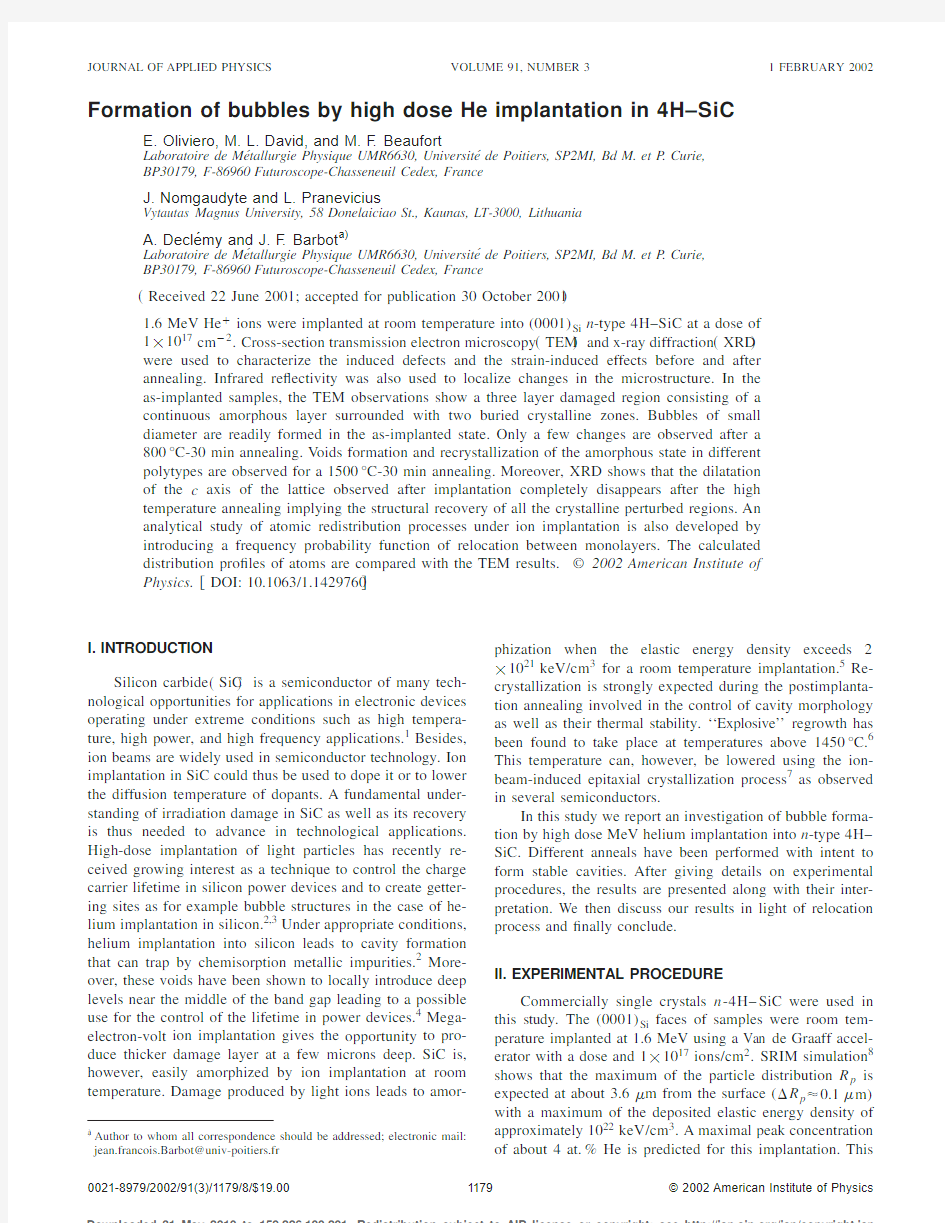
A low magni?cation cross-sectional TEM image aligned near a?112ˉ0?direction shows that helium implanted at a dose of1?1017cm?2produces a continuous damaged layer of approximately650nm in width at about3.6?m deep below the surface,as expected from SRIM calculations.A closer view shows that this damaged band is made up of three different regions denoted by A,
B and
C in Fig.1.A selected area diffraction pattern of the B layer shows a halo pattern corresponding to the amorphous phase while A and C are crystalline4H–SiC.The400-nm-wide amorphous region B can be divided in two regions B1and B2.The B1region is related to the presence of small bubbles,1–2nm in diameter whereas the B2part does not show any visible defects.Their widths are about280and120nm,respectively.However, contrary to what can be observed in implanted silicon under the same implant conditions,zones of dark contrast,A and C, are found outside the central band B.The black contrast observed in theses surrounding layers may result from de-fects not resolvable by TEM.The A band,lying in front of the B layer,shows a wider extent?170nm?and a lower defect density than the C one located below?55nm?.The C band also contains some small bubbles whereas no bubble is visible in the A band.High dose implantation of helium at room temperature into SiC thus produces small bubbles lo-cated rather at the end of the damage layer.A similar damage structure has already been reported in6H–SiC implanted at 650°C with180keV O?.9The authors argue that this is a consequence of the elastic loss pro?le and of in situ defect annealing during implantation.Previous studies10,11on irra-diated6H–SiC with1MeV He ions at2?1017cm?2al-ready report the presence of an amorphous buried layer in the region where the elastic loss exceeds the critical value of2?1021keV/cm3.They also report the observations of defect clustering in the regions adjacent to the amorphous band. However,they do not mention any bubble formation.In hot-pressed4H–and6H–SiC,observations of platelets have been reported for implantation of2450at.ppm He.12These platelets of9nm in diameter do not show any major evolu-tion until1100°C anneals.Platelets have also been observed for hydrogen implantations using similar conditions but after annealing only.13In case of high implanted doses,we do not observe any platelets of cavity type but bubbles and point defect clusters.The same behavior also occurs in6H–SiC since we only observe prismatic loops after a2?1016He cm?2implantation followed by an annealing at 800°C.14
Figure2shows an x-ray diffraction experiment in sym-metrical position??,2??for the?0008?Bragg re?ection.Two peaks are clearly observed:a sharp peak due to the unper-turbed SiC and a broadened peak,toward the low angle side, ascribes to an oriented dilatation along the c-axis lattice in-side the crystalline perturbed regions.The mean value of the dilatation is calculated using
?c
c
??ctg????1?
and is found to be?5?10?3.This dilatation could be as-cribed to clustering of interstitials in the?0001?plane and/or to the stress induced by the amorphous layer of lower den-sity.
The FTIR spectrum exhibits an interference pattern as shown in Fig.3,relative to the weak modi?cation of the optical refractive index n of the implanted layer.The position of the perturbed band d is calculated
using
FIG.1.Cross-sectional TEM image of4H–SiC subjected to room tempera-ture helium implantation?1.6MeV,1?1017cm?2,no anneal?.In the inset, diffraction pattern of the B zone?amorphous state?.
d ?
1
2n ?f
,?2?
where ?f is the spacing between two re?ectance minima.With a mean value of ?f ?450cm ?1and taking 15n (SiC)?3.1we obtain d ?3.6?m.This value is consistent with SRIM calculations.
B.Observations after annealing at 800°C for 30min
As observed before annealing,a closer view on the dam-aged layer annealed at 800°C for 30min,Fig.4shows three different regions,also labeled A,B,and C.In the B region,no TEM change is observed after annealing.As seen previ-ously,this central region is still amorphous and can be di-vided into two parts:B 1where numerous small bubbles are still present and B 2region free of bubbles ?see Fig.5?.Con-cerning the A and C regions,however,we note that their widths and interface appearances have changed.The A and C layers expand,respectively,over 300and 65nm,which leads to a 765nm damaged layer.For oneself,it seems that all the interfaces are relatively sharper and that the size and density of residual defects in both these outside layers are more im-
portant than in the as-implanted sample,Fig.1.Numerous small bubbles are still present in the C region as those pointed out by an arrow in Fig.5.A microdiffraction pattern show that the A and C regions are single crystalline SiC.Figure 6shows a set of high resolution TEM images taken outside the damage region ?Fig.6?a ??and next to the a /c interface between the B and A regions ?Fig.6?b ??and be-tween the B and C regions ?Fig.6?c ??.In the region located in front of the buried layer,Fig.6?a ?,we observe a period-icity of straight fringes of about 1.005nm corresponding to the lattice constant of 4H–SiC along the ?0001?direction,as expected.Near the a /c interface the fringes become wavy.
In
FIG.2.X-ray ?0008?Bragg re?ection for the unimplanted 4H-SiC ?spot line ?and implanted 1.6MeV ,1?1017cm ?2sample ?solid line ?
.
FIG. 3.IR spectra for the unimplanted sample ?dashed line ?and as-implanted 4H–SiC ?solid line ?
.
FIG.4.Cross-sectional TEM image of 4H–SiC subjected to room tempera-ture helium implantation ?1.6MeV ,1?1017cm ?2?and annealing ?800°C,30min ?
.
FIG.5.Closer view of the damaged band ?B1and C regions ?for the visu-alization of the bubbles ?1.6MeV ,1?1017cm ?2,800°C 30min ?.In the inset,the diffraction pattern shows an halo corresponding to the amorphous state ?B1?and diffraction dots due to the crystalline region ?C ?.
Fig.6?b ?,we see that the transition of amorphous ?B ?to crystalline SiC ?A ?takes place on 30nm since small islands of crystalline SiC are visible up to this value.Numerous stacking faults are present in these crystalline regions.The C region mainly consists of defects like stacking faults perpen-dicular to the ?0001?direction,Fig.6?c ?.
The effect of the 800°C–30min annealing on the x-ray diffraction curve is shown in Fig.7.The perturbed diffrac-tion peak toward the low angle side becomes,after anneal-ing,a wide plateau that corresponds to dilatations ?c /c ex-tending from 3to 6.5?10?3.After annealing,FTIR spectrum of the sample still exhibits an interference pattern with few modi?cations in comparison with the as-implanted sample.These modi?cations are ascribed to the weak widen-ing of the buried layer as observed by TEM.
These observations are consistent with previous studies 16where only a small recovery of the damaged layer is ob-served after a 800°C 30min annealing performed on a 6H–
SiC sample implanted with 8MeV Si 3?ions at a dose of 1?1017cm ?2.
C.Annealing at 1500°C for 30min
Figure 8shows a cross-sectional TEM image after a 1500°C annealing for 30min.The buried layer width is now reduced to 400nm.A low density of small defects is still observed on both sides.These defects extend up to the sur-face but to only a few hundred nm into the bulk.The buried layer contains bubbles and can be divided in three different regions denoted a1,b1,and c1.In the central region b1of 150nm width,columns of black contrast slightly inclined from the substrate ?0001?are observed,Fig.9.In the a1and c1parts of 150and 100nm width respectively,columns of black contrast appear perpendicular to the ?0001?direction.Selected area diffraction pattern,see the inset of Fig.9,
does
FIG.6.Set of high resolution TEM images taken ?a ?outside the damage region,?b ?next to the a /c interface in the B1region ?upper part ?,?c ?next to the a /c interface in the C region ?lower part ?
.
FIG.7.X-ray ?0008?Bragg re?ection for the implanted 4H–SiC ?solid line ?and annealed 800°C-30min ?spot line ?
.
FIG.8.A bright ?eld image in under-focus condition of the 1500°C an-nealed sample ?30min ?.Visualization of the bubbles.
not present any halo pattern showing the complete recrystal-lization of the amorphous layer during this 1500°C anneal-ing.The (1
ˉ10)pattern of 3C–SiC is observed besides the lattice spots due to the 4H–SiC.A circle marks the 111and the equivalent re?ections.The ?111?direction of 3C–SiC coincides with the ?0001?direction of 4H–SiC and the other ?111
ˉ?with the ?1ˉ102?.This clearly shows that the 3C–SiC has grown epitaxially on the 4H–SiC.Diffuse streaks are also observed on the diffraction pattern in Fig.9and are attributed to the presence of stacking faults.The epitaxial regrowth initiates from the a /c interfaces leading to the for-mation of the a1and c1regions and is followed by columnar growth of 4H–SiC and epitaxial growth of 3C–SiC leading to the formation of the b1region.The mechanism of this polytypism transition during annealing is not yet understood.Similar behavior has been observed in MeV-ion implanted 6H–SiC followed by a 1000°C annealing.16The atomic con-?guration for the recrystallization during annealing is pro-posed in Fig.10.In this con?guration the (1
ˉ102)plane of layer-by-layer 4H–SiC coincides with the ?0001?plane of columnar 4H–SiC.The bond mismatches existing at the in-terface between the columnar and layered regions may lead to the formation of numerous stacking faults as observed.The latter are known to have a low energy formation into SiC,?4H ?14.7?2.5mJ m ?2.17
It is likely that upon annealing at 1500°C the He out-gases from the sample.Although no helium release experi-ment has been reported yet in SiC,we will consider in the following that bubbles are empty of He and thus will be named cavities or voids.
The bright ?eld image in under-focus condition of Fig.8shows numerous cavities distributed all over the buried layer
in contrast to what is mentioned above after the 800°C an-nealed sample ?Fig.4?where bubbles are present only in a part of the B layer.Obviously,the 1500°C anneal also en-larges the cavities.Their size,shape,and density are found to depend on their localization in the layer.In the center of the band,the cavities have a rather circular shape with a size ranging from 15to 50nm or are faceted with facets along the ?1ˉ
100?and ?0001?directions.Toward the implanted surface,they become smaller and in the last 150nm they appear
cylindrical in the ?1ˉ100?direction.The density does not seem to vary (?1016
/cm 3).In the a1region,no cavities are observed directly after implantation and even after the 800°C anneal.Below the center of the band,in the c1re-gion,the cavity density increases roughly by a factor 2whereas their size decreases.They are circular or slightly elongated with a diameter in the range 5–25nm.This cavity band ends with a row of large faceted cavities ??30nm ?.We do not observe dislocation loops,contrary to what was expected from a previous study.10The authors mention that cavities are always accompanied by faulted dislocation loops of interstitial type.The used doses,however,are smaller than the one implanted in this study.
In the x-ray diffraction spectrum,the satellite diffraction peak observed before annealing has disappeared.The IR re-?ectivity spectrum exhibits an interference pattern as seen before,that is coherent with TEM observations.Indeed,no great variation of the width of the perturbed band that
corre-
FIG.9.Bright ?eld image of the recrystallization layer after the implanta-tion and the 1500°C annealing.In the inset,diffraction pattern of the dam-aged band.As seen the ?0001?4H–SiC correspond to the ?111?
3C–SiC.
FIG.10.Model for the atomic con?guration of the recrystallization ob-served after the 1500°C annealing.
sponds to the optical interface located at about3.6?m from the surface is observed.These observations show an almost
complete structural recovery of the initially perturbed crys-
talline regions of the as-implanted sample.
D.In situ annealing
An in situ annealing experiment has been performed in
the JEOL200CX.The starting temperature for observations
was350°C and the?nal was820°C.During the in situ an-
nealing,no clearly visible change on the bubble size has
been seen in the amorphous zone?B?.At the end of the
annealing experiment,the buried layer can also be divided in
three different regions A,B,and C.The amorphous central
region B,280nm thick,is a continuous layer of small cavi-
ties whereas the two outside regions,A and C,contain small
defects.We note that the A region shows a higher density of
defects near the a/c interface.When comparing with the
800°C annealing?Sec.III B?we note that this region corre-
sponds to the amorphous region?B2?,i.e.,the one with no
bubbles.This suggests that the electron beam induces the
epitaxial regrowth of this layer.No growth occurs on the
deeper a/c interface showing that the bubbles stabilize the
amorphous layer.The recovery of defects under ion beam is
clearly shown in the deeper band C since no dark contrast
spot is present near the edge of the sample.
IV.MODELIZATION OF THE DAMAGED STRUCTURE TEM investigations of the damage induced by
1017ions/cm2He implantation at1.6MeV in4H–SiC show
that a three layer structure can be distinguished:two outside
layers which mainly consist of point defect clusters and an
amorphous layer in the middle.Similar results have been
reported for heavier ions.9,18Even after high temperature an-
nealing,a three layer structure is still observed.
A.Derivation
To model our observations,i.e.,the damaged structure in
layers,we consider the transport of atoms within the colli-
sional area and their relocations under ion bombardment.
The mathematical formalism of mass transport in two ele-
ment solids was developed and applied in the case of metals ?Sigmund approach?.It is based on the solutions of the non-linear integrodifferential mixing equation.19,20In this paper
we consider a simpli?ed calculation by introducing the relo-cation function w i(K,L)that de?nes the frequency probability of relocation of i atoms from the K th to the L th monolayer; the solid being divided into layers of equal thickness h0. Thus,the time variation of concentration for i th type atoms in the K th monolayer is described by
dc i?K?dt ??L?1
?
w i?L,K?c i?L???L???
?
w i?K,L?c i?K?.?3?
The?rst term of Eq.?3?gives the?ux of i atoms arriving into the K th monolayer and the second term describes the ?ux of i atoms leaving the K th monolayer?the negative val-ues of L including zero give the possibility of i atoms to go out of the solid?.Since the relocated atoms are forming Fren-kel pairs,and because of the nonhomogeneous distribution of energy losses,atoms are transferred to the periphery of the activated region.It results in an excess of vacancies in the R p region and an excess of interstitials in the periphery.The?ux of atoms driven out of the activated area is given by Fick’s law:
F i??
??c i D i?
?x??D i
?c i
?x?c i
?D i
?x.?4?where D i is the diffusion coef?cient of i atoms that can be written in the form
D i?16?i2w i?x?,?5??i(?h0)being the jump distance and w i(x)the displace-ment frequency which is supposed to be proportional to the nuclear energy losses(dE/dx)n given by SRIM calculations. In the case of SiC,because of the very small diffusion coef-?cient D i at moderate temperature,the?rst term of Eq.?4?can be neglected and the?ux of atoms?balistic relocation?initiated by displacement processes can be rewritten as
F i?
?
?x?dE dx
?
n
.?6?
From Eq.?6?different areas in the SiC damaged zones can be distinguished.When the displacement rate is maxi-mum?around R p?the?ux of redistributed atoms approaches zero
?
?x?dE dx
?
n
?0,
i.e.,?uxes in and out are compensated.This zone can thus be considered as an area highly enriched by vacancies and in-terstitials.In the areas where
?
?x?dE dx
?
n
is maximum(R p??R p)atomic motion takes place,i.e.,the ?ux of relocated atoms approaches maximum value.From the viewpoint of point defects the region above the region of maximum displacement rate is enriched in vacancies while the region behind is enriched by interstitials and is not highly affected by displacements.Thus,differences are expected af-ter subsequent annealing.
In this work,the relocation function w i(K,L)is de?ned as
w i?L,K??W i0exp??12
?h0?K?1??R p
?R p?2
?
1
2?h0?K?L?l i
?2?,?7?
where W i0is a constant proportional to the?ux of incident ions and dependent on the energy of ions.As seen from Eq.?7?,w i(L,K)results in the product of the probability of reloca-tion between K and L monolayers with the displacement rate, which is proportional to the nuclear energy losses.l i is an adjustable parameter characteristic of the relocation length for i atoms.
B.Simulations and comparison with experimental results
The variations of concentration for the i th atoms are shown in Fig.11as a function of depth with regards to R p for two different values of the diffusion coef?cient D .The curves are normalized with ?i ?1n c i ?1for an unperturbed monolayer.To take into account the skewness of the nuclear energy loss pro?le,two straggling values ?R p 1?above R p ?and ?R p 2?behind R p ?are distinguished according to the SRIM calculations.Since the displacement rate of Si (i ?1)and C (i ?2)atoms depends on their threshold dis-placement energy in the crystal sites,two different displace-ment rates W i 0evaluated from SRIM calculations are taken into account although that leads to only few modi?cations of the curves.Figure 11shows that three different regions can be distinguished and that transport of atoms exists from the highly perturbed area to the periphery.The central region shows an excess of vacancies while excess of interstitials appears on both sides.As the temperature increases,the irra-diated system tends to relax via atomic movement and dif-ferences in concentration become less pronounced.It is dif-?cult to compare the width of the regions with those obtained from TEM results since the TEM resolution does not allow us to detect point defects.However,the curves predict two outside layers of different widths and different concentrations of point defects in agreement to what is ob-served by TEM.Moreover,the highly damaged zone with excess of vacancies corresponds to the amorphous zone ?la-beled B ?including the bubbles.The difference is also mani-fest after annealing ?1500°C ?where the periphery regions recrystallize epitaxially whereas the central one consists of differently oriented crystallites with equiaxed structure ?Fig.9?.Moreover,when comparing to TEM results,we see that large and circular cavities are formed in the area of R p where ?ux of atoms is nearly zero.
Our calculations predict a ballistic displacement of at-oms.SiC being a two component target,ballistic mobilities of Si and C atoms differ and redistribution of the two com-ponents under irradiation is expected,leading to the forma-tion of new phases,as carbon graphite for example.This has already been reported in oxygen-ion-implanted silicon where compositional ?uctuations in the damaged zone have been observed.Carbon atoms have been found to accumulate in the periphery of the buried amorphous zones.21,22Composi-tion changes have also been reported in Ar-bombarded SiC.23This will be the next step of our calculations.V.CONCLUSIONS
Implantation at room temperature of high dose helium ions into SiC leads to the formation of small bubbles.How-ever,the critical dose for forming bubbles exceeds the dose for amorphization and a multilayer structure is observed;an amorphous layer surrounded by crystalline zones of point defects.Only a slight recovery of the damaged layer is ob-served after an 800°C-30min annealing.No change in bubble morphology is observed.The in situ annealing shows that the electron beam induces the epitaxial regrowth of the amorphous layer only from the upper interface in the region free of bubbles.The presence of bubbles in the other amor-phous region prevents the electron beam induced recrystalli-zation.At higher temperature ?1500°C ?recrystallization take place resulting in a complex structure with inclusions of ep-itaxial 3C–SiC and columnar growth of 4H–SiC.The 1500°C anneal relax the structure and enlarges the cavities.However,their size,shape,and density are found to be dif-ferent depending on their localization in the damaged band.
Simultaneously,the multilayered structure is analyzed using a mathematical formalism considering the atomic relo-cations between monolayers.It is shown that atomic dis-placements initiate mass transport.By comparing the calcu-lated pro?les with the TEM results we note that the circular bubbles are formed where ?ux of atoms initiated by displace-ment processes is negligible whereas smaller bubbles ?or voids ?and epitaxial recrystallization occur in the region of excess interstitials where the ?ux is maximum.ACKNOWLEDGMENTS
The authors would like to acknowledge E.Ntsoenzok,CERI-CNRS,France for the implantations and R.Job,FeU-Hagan,Germany for the high temperature annealing.
1M.A.Capano and R.J.Trew,Mater.Res.Bull.19–20,19?1997?.
2
D.M.Follstaedt,S.M.Myers,C.A.Petersen,and J.W.Medernach,J.Electron.Mater.25,157?1996?.3
V .Raineri,P.G.Fallica,G.Percolla,A.Battaglia,M.Barbagallo,and S.U.Campisano,J.Appl.Phys.78,3727?1995?.4
V .Raineri,P.G.Fallica,and S.Libertino,J.Appl.Phys.79,9012?1996?.5
J.A.Spitznagel,S.Wood,W.J.Choyke,N.J.Doyle,J.Bradshaw,and S.G.Fishman,Nucl.Instrum.Methods Phys.Res.B 16,237?1986?.6
C.J.McHargue and J.M.William,Nucl.Instrum.Methods Phys.Res.B 80?81,889?1993?.7V .Heera,J.Stoemenos,R.Ko ¨gler,and W.Skorupa,J.Appl.Phys.77,2999?1995?.8
J.F.Ziegler,J.P.Biersack,and U.Littmark,The Stopping and Range of Ions in Solids ?Pergamon,New York,1985?
.
FIG.11.The concentration pro?les of atoms after implantation calculated for two values of the diffusion coef?cient D ?D ?0:before annealing,D ?6?10?4:after high temperature annealing ?.?R p 1?0.4?m and ?R p 2?0.1?m are taken from SRIM calculations and re?ect the inhomogeneous displacement rate of atoms.l i is the characteristic relocation length of i -type atoms and w i 0is the displacement rate depending on the threshold displace-ment energy ?i ?1for Si atoms and i ?2for C atoms ?.
9M.Ishimaru,R.M.Dickerson,and K.E.Sickafus,Appl.Phys.Lett.75, 352?1999?.
10M.G.Grimaldi,L.Calcagno,P.Musumeci,N.Frangis,and J.Van Landuyt,J.Appl.Phys.81,7181?1997?.
11N.Frangis,J.Van Landuyt,M.G.Grimaldi,and L.Calcagno,Nucl. Instrum.Methods Phys.Res.B120,186?1996?.
12J.Chen,P.Jung,and H.Trinkaus,Phys.Rev.B61,12923?2000?.
13J.Grisolia,F.Cristiano,B.De Mauduit,G.Ben Assayag,F.Letertre,B. Aspar,L.Di Cioccio,and A.Claverie,J.Appl.Phys.87,8415?2000?. 14E.Oliviero,M.F.Beaufort,A.Declemy,G.Blondiaux,E.Nstoenzok,and J.F.Barbot,MRS Boston?2000?.
15G.L.Harris,Properties of Silicon Carbide?INSPEC,London,1995?. 16M.Ishimaru,S.Harada,T.Motooka,T.Nakata,T.Yoneda,and M.Inoue, Nucl.Instrum.Methods Phys.Res.B127?128,195?1997?.17M.H.Hong,A.V.Samant,and P.Pirouz,Philos.Mag.A80,919?2000?. 18Y.Pacaud,W.Skorupa,A.Perez-Rodriguez,G.Brauer,J.Stoemenos,and R.C.Barklie,Nucl.Instrum.Methods Phys.Res.B112,321?1996?.
19P.Sigmund and A.Oliva,Nucl.Instrum.Methods Phys.Res.B82,269?1993?.
20M.W.Sckerl,https://www.doczj.com/doc/bc3457746.html,m,and P.Sigmund,Nucl.Instrum.Methods Phys. Res.B140,75?1998?.
21N.P.Barradas,C.Jeynes,and S.M.Jackson,Nucl.Instrum.Methods Phys.Res.B136?138,1168?1998?.
22M.Ishimaru,R.M.Dickerson,and K.E.Sickafus,J.Electrochem.Soc. 147,1979?2000?.
23A.Miotello,L.Calliari,R.Kelly,https://www.doczj.com/doc/bc3457746.html,idani,M.Bonelli,and L.Guzman, Nucl.Instrum.Methods Phys.Res.B80?81,931?1993?.