TPA3116D2 PDF
- 格式:pdf
- 大小:1.40 MB
- 文档页数:34
“HiFi毁⼀⽣”,从⼊烧到退烧你需要⼊⼿的⾳箱都在这了近两年,多媒体有源⾳箱在中国市场的发展势头很猛,随着⽤户对于⾳质的追求越来越⾼,进⼀步推动了中⾼端有源⾳箱市场的发展。
在今年7⽉中旬的时候,我们曾针对⽬前中国有源⾳箱市场的发展现状发起了⼀项⼩调查,主要是为了了解当前中国消费者对有源⾳箱市场在各类问题上的真实看法和诉求。
有趣的是,在围绕产品展开的相关问题上,有⼀项投票结果让我们感到很意外:⽹友对桌⾯HiFi⾳箱的关注度,远远⾼于蓝⽛⾳箱、AI智能⾳箱和电视⾳响,甚⾄⽐传统桌⾯有源⾳箱的关注度还要⾼出22个百分点,以51.6%的投票数⾼居有源⾳箱类型关注榜⾸位。
这样的结果也反映出,⽤户对于⾳质的要求⼀直都处于上升趋势。
对于⼀款⾳箱来说,只有⾳质好,才能真正打动⽤户的⼼。
然⽽,⽬前市⾯上的桌⾯HiFi⾳箱种类繁多,但绝⼤多数消费者⼜没有条件去试听每⼀款⼼仪的产品,所以经常会为⼊⼿哪⼀款⾳箱⽽苦恼。
当然我们也早已发现这⼀问题,所以今天借着这个机会,我们将按照从⼊门发烧到⾼端HiFi系统的进阶顺序,由浅⾄深地为⼤家推荐值得⼊⼿的精品。
不论你是初烧⾳乐爱好者还是多年的⽼烧⽤户,相信都能在今天这篇精品推荐中,找到属于你的那款桌⾯HiFi⾳箱。
—1—初烧⼩⽩怎么选?千元国产精品给你好听百元价位经典之作:惠威D1080-IVB书架⾳箱对于那些刚刚步⼊初烧阶段的⾳乐爱好者来说,他们⼿上或许没有太多预算,但同时⼜希望能够提升⾳乐体验。
其实⽬前这类⽤户的数量相当庞⼤,他们也代表了⼤多数普通⾳乐爱好者对影⾳娱乐体验的需求。
所以针对这部分⽤户,我们今天推荐的第⼀款产品是来⾃于惠威的D1080-IVB,它是惠威D1080经典系列的⾼端升级版书架⾳箱,于2016年上市,售价860元。
惠威D1080-IVB书架⾳箱单元⽅⾯,惠威D1080-IVB使⽤20mm⾦属球顶⾼⾳单元,中低⾳单元则使⽤了惠威经典之作--M200MKIII的5英⼨中低⾳单元,中频饱满醇厚,低频下潜有⼒。
ProductFolderSample &BuyTechnicalDocumentsTools &SoftwareSupport &CommunityTPA3116D2,TPA3118D2,TPA3130D2ZHCS891D–APRIL2012–REVISED JANUARY2015 TPA3116D2具有AM干扰抑制功能的15W、30W、50W无滤波器D类立体声放大器系列1特性3说明•支持多种输出配置TPA31xxD2系列器件是用于驱动扬声器的高效立体声数字放大器功率级,单声道模式下的驱动功率高达–21V电压、4Ω桥接负载(BTL)负载条件下的功率为2×50W(TPA3116D2)100W/2Ω。
TPA3130D2的效率非常高,无需外部散–24V电压、8ΩBTL负载条件下的功率为2×热器即可在单层PCB板上提供2×15W的功率。
30W(TPA3118D2)TPA3118D2甚至可以在不使用外部散热器的情况下在–15V电压、8ΩBTL负载条件下的功率为2×双层PCB上提供2×30W/8Ω的功率。
如果需要更高15W(TPA3130D2)的功率,可以选用TPA3116D2,这款器件在其顶层•宽电压范围:4.5V至26V PowerPAD上连接一个小型散热器后可提供2ו高效D类运行50W/4Ω的功率。
所有这三款器件均使用同一种封–兼具>90%的功率效率与低空闲损耗特性,大装,这样一来,使用同一个PCB板即可满足不同功率幅减小了散热器尺寸级的需求。
–高级调制系统配置TPA31xxD2高级振荡器/PLL电路采用多开关频率选项•多重开关频率来抑制AM干扰;搭配使用主从模式选项时,还可使–AM干扰防止多个器件实现同步。
–主从模式同步–高达1.2MHz的切换频率TPA31xxD2器件针对短路、过热、过压、欠压和直流•采用具有高PSRR的反馈功率级架构,降低了等故障提供了全面保护。
TPA3116D2 具有AM干扰抑制功能得15W、30W、50W无滤波器D类立体声放大器系列特性支持多种输出配置21V电压、4Ω桥接负载(BTL) 负载条件下得功率为2×50W (TPA3116D2) 24V 电压、8ΩBTL负载条件下得功率为2×30W(TPA3118D2)15V电压、8ΩBTL 负载条件下得功率为 2 ×15W(TPA3130D2)宽电压范围:4、5V 至26V高效 D 类运行兼具>90%得功率效率与低空闲损耗特性,大幅减小了散热器尺寸高级调制系统配置,多重开关频率,AM干扰防止,主从模式同步高达1、2MHz得切换频率采用具有高PSRR 得反馈功率级架构,降低了PSU 需求可编程功率限制,差分与单端输入立体声模式与单声道模式(采用单滤波器单声道配置)由单电源供电运行,减少了元件数量集成了具有错误报告功能得自保护电路,其中包括过压、欠压、过热、直流检测与短路等保护,耐热增强型封装DAD(32 位引脚散热薄型小外形尺寸(HTSSOP) 封装,焊盘朝上)DAP(32 位HTSSOP 封装,焊盘朝下)-40°C至85°C环境温度范围应用小型-微型组件、扬声器、扩展坞底座汽车售后阴极射线管(CRT) TV消费类音频应用说明TPA31xxD2系列器件就是用于驱动扬声器得高效立体声数字放大器功率级,单声道模式下得驱动功率高达100W/2Ω、TPA3130D2 得效率非常高,无需外部散热器即可在单层PCB板上提供2×15W得功率。
TPA3118D2甚至可以在不使用外部散热器得情况下在双层PCB 上提供 2 ×30W/8Ω得功率。
如果需要更高得功率,可以选用TPA3116D2,这款器件在其顶层PowerPAD 上连接一个小型散热器后可提供2×50W/4Ω得功率。
所有这三款器件均使用同一种封装,这样一来,使用同一个PCB 板即可满足不同功率级得需求。
ProductFolderSample &BuyTechnicalDocumentsTools &SoftwareSupport &CommunityTPA3251D2ZHCSDT9C–JUNE2015–REVISED JUNE2015 TPA3251D2175W立体声/350W单声道PurePath™超高清模拟输入D类放大器1特性•采用推荐的系统设计时,符合电磁干扰(EMI)标准•差分模拟输入2应用•总谐波失真+噪声(THD+N)为10%时的总输出功•蓝光碟磁盘™/DVD接收器率•高端HTiB系统–175W/4Ω,桥接负载(BTL)立体声配置•AV接收机–220W/3Ω,桥接负载(BTL)立体声配置•高端条形音箱–350W/2Ω,并行桥接负载(PBTL)单声道配置•微型Combo系统•THD+N为1%时的总输出功率•有源扬声器和低音炮–140W/4Ω,BTL立体声配置–175W/3Ω,BTL立体声配置3说明–285W/2Ω,PBTL单声道配置TPA3251D2是一款高性能D类功率放大器,它具有•采用高级集成反馈设计,具有高速栅极驱动器错误D类效率并且能够带来真正的高端音质。
该器件特有校正功能高级集成反馈设计和专有高速栅极驱动器错误校正功能(PurePath™超高清)(PurePath™超高清)。
该技术可使器件在整个音频–高达100kHz的单宽带,用于高清(HD)源的高频带内保持超低失真,同时展现完美音质。
该器件最频成分多可驱动2个175W/4Ω负载和2个220W/3Ω负载,–超低THD+N:1W/4Ω时为0.005%;削波时<0.01%并且特有一个2VRMS模拟输入接口,支持与高性能–60dB电源抑制比(PSRR)(BTL,无输入信DAC(例如,TI的PCM5242)的无缝连接。
除了出号)色的音频性能外,TPA3251D2还兼具高功率效率和超–<60µV(A加权)输出噪声低功率级空闲损耗(1W以下)两大优点。

T P A3116D2中文数据表(总23页)-CAL-FENGHAI.-(YICAI)-Company One1-CAL-本页仅作为文档封面,使用请直接删除TPA3116D2 具有AM 干扰抑制功能的15W、30W、50W无滤波器D类立体声放大器系列特性支持多种输出配置21V 电压、4Ω桥接负载 (BTL) 负载条件下的功率为 2 × 50W (TPA3116D2)24V 电压、8Ω BTL 负载条件下的功率为 2 × 30W (TPA3118D2)15V 电压、8Ω BTL 负载条件下的功率为 2 × 15W (TPA3130D2)宽电压范围:至 26V高效 D 类运行兼具 > 90% 的功率效率与低空闲损耗特性,大幅减小了散热器尺寸高级调制系统配置,多重开关频率,AM 干扰防止,主从模式同步高达的切换频率采用具有高 PSRR 的反馈功率级架构,降低了 PSU 需求可编程功率限制,差分和单端输入立体声模式和单声道模式(采用单滤波器单声道配置)由单电源供电运行,减少了元件数量集成了具有错误报告功能的自保护电路,其中包括过压、欠压、过热、直流检测和短路等保护,耐热增强型封装DAD(32 位引脚散热薄型小外形尺寸 (HTSSOP) 封装,焊盘朝上)DAP(32 位 HTSSOP 封装,焊盘朝下)-40°C 至 85°C 环境温度范围应用小型-微型组件、扬声器、扩展坞底座汽车售后阴极射线管 (CRT) TV消费类音频应用说明TPA31xxD2 系列器件是用于驱动扬声器的高效立体声数字放大器功率级,单声道模式下的驱动功率高达 100W/2Ω。
TPA3130D2 的效率非常高,无需外部散热器即可在单层 PCB 板上提供 2 × 15W 的功率。
TPA3118D2 甚至可以在不使用外部散热器的情况下在双层 PCB 上提供 2 × 30W/8Ω的功率。
28 \China Science & Technology Education∙研究背景摩尔斯电码(Morse code)是一种以信号通断的时间长短和组合方式传输信息的信号代码。
本人在进行科技活动课和信息技术课教学过程中,将摩尔斯电码收发报的知识和体验活动引入课堂。
学生对摩尔斯电码很感兴趣,但是在学生学习完理论课程以后,我却没法找到合适的、仿真度高的教具和学具让学生体验摩尔斯电码收发报过程。
所以,很有必要设计一套仿真度高的摩尔斯电码收发报体验设备用于装备学校实验室和课堂。
∙项目研究过程 确定项目研究目标本项目研究的目标,是研究一种方法和相关的设备,便于师生在课堂上灵活地分组开展高仿真度的莫尔斯电码收发实验。
该项目必须实现如下目标:①设备成本低廉,便于师生动手制作和使用;②可灵活方便地分组学习;③不会对外发射大功率高频无线电波,不干扰别的电子设备,无须考取业余无线电台操作证书就可以操作;④可自动收发和自动编解码,可对使用者的电码输入作检查与测评;⑤设备外形与使用方法、使用效果具有高度仿真性。
规划系统各部分的组成架构摩尔斯电码无线通讯仿真实验室的总体架构设计为:实验室里的所有学生组成1个或多个学习小组,以小组形式开展学习活动的科普课堂模式,每个学习小组采用一发一收或一发多收的形式,轮流开展收发摩尔斯电码的活动。
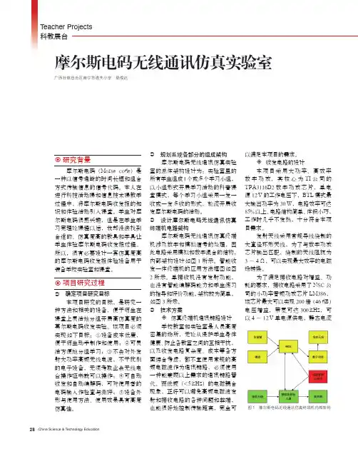
设计摩尔斯电码无线通讯仿真终端机电路架构摩尔斯电码无线通讯仿真终端机涉及数字和模拟信号的处理,因此电路采用模拟和数字混合的结构,内部架构设计如图1所示。
智能收发一体终端机的应用方法框图如图2所示。
单接收机没有发射功能,也没有智能编解码能力和学生练习的指导和评价功能,架构较为简单,如图3所示。
技术方案仿真终端机通讯链路设计学校教室和实验室是人员高度密集的场所,无论从保护学生身体健康、防止各教室之间的互相干扰,以及收发电路复杂度、成本等各方面综合考虑,都不宜使用常规的高频电磁波作为通讯链路,必须使用一种能兼顾以上需求的通讯链路替代。

TITPA3116D22x50WD绫婚煶棰戞斁澶у櫒瑙e喅鏂规TI鍏徃鐨凾PA31xxD2绯诲垪鏄珛浣撳0楂樻晥鏁板瓧鍔熺巼鏀惧ぇ鍣?鑳介┍鍔?娆у鎵0鍣ㄩ珮杈?00W.宸ヤ綔鐢靛帇4.5 V – 26 V,鏁堢巼澶т簬90%,TPA3130D2鐨勯珮鏁堢巼鍙噰鐢ㄥ崟灞侾CB,涓嶇敤鏁g儹鍣ㄦ彁渚?x15W杈撳嚭鍔熺巼, TPA3118D2閲囩敤鍙屽眰PCB, 涓嶇敤鏁g儹鍣ㄦ彁渚?x30W/8娆у杈撳嚭鍔熺巼, TPA3116D2閲囩敤灏忓瀷鏁g儹鍣ㄥ彲鎻愪緵2x50W/4Ω杈撳嚭鍔熺巼,涓昏鐢ㄤ簬灏?寰瀷鍏冧欢鐨勬潯褰㈤煶绠?鍚庡競鍦烘苯杞︾數瀛?CRT TV鍜屾秷璐圭被闊抽.鏈枃浠嬬粛浜員PA31xxD2涓昏鐗规€?鏂规鍥? 搴旂敤鐢佃矾鍥句互鍙婅瘎浼版澘TPA3116D2EVM涓昏鎸囨爣,鐢佃矾鍥?鏉愭枡娓呭崟鍜孭CB甯冨眬鍥?The TPA31xxD2 series are stereo efficient, digital amplifier power stage for driving speakers up to 100W/2Ω in mono. The high efficiency of the TPA3130D2 allows it to do 2x15W without external heat sink on a single layer PCB. The TPA3118D2 can even run 2x30W/8Ω without heat sink on a dual layer PCB. If even higher power is needed the TPA3116D2 does 2x50W/4Ω with a small heat-sink attached to its top side PowerPad. All three devices share the same footprint enabling a single PCB to be used across different power levels.The TPA31xxD2 advanced oscillator/PLL circuit employs a multiple switching frequency option to avoid AM interferences; this is achieved together with an option of Master/Slave option, making it possible to synchronize multiple devices.The TPA31xxD2 devices are fully protected against faults with short-circuit protection and thermal protection as well as over-voltage, under-voltage and DC protection. Faults are reported back to the processor to prevent devices from being damaged during overload conditions.TPA31xxD2涓昏鐗规€?Supports Multiple Output Configurations2×50-W into a 4-Ω BTL Load at 21 V (TPA3116D2)2×30-W into a 8-Ω BTL Load at 24 V (TPA3118D2)2×15-W into a 8-Ω BTL Load at 15 V (TPA3130D2)Wide Voltage Range: 4.5 V – 26 VEfficient Class-D Operation>90% Power Efficiency Combined with Low Idle LossGreatly Reduces Heat Sink SizeAdvanced Modulation SchemesMultiple Switching FrequenciesAM AvoidanceMaster/Slave SynchronizationUp to 1.2 MHz Switching FrequencyFeedback Power Stage Architecture with High PSRR Reduces PSU RequirementsProgrammable Power LimitDifferential/Single-Ended InputsStereo and Mono Mode with Single Filter Mono ConfigurationSingle Power Supply Reduces Component CountIntegrated Self-Protection Circuits IncludingOver-Voltage, Under-Voltage, Over-Temperature, DC-Detect, andShort Circuit with Error ReportingThermally Enhanced PackagesDAD (32-pin HTSSOP Pad-up)DAP (32-pin HTSSOP Pad-down)–40鈩?to 85鈩?Ambient Temperature RangeTPA31xxD2搴旂敤:Mini-Micro Component, Speaker Bar, DocksAfter-Market AutomotiveCRT TVConsumer Audio Applications鍥?. TPA31xxD2绯诲垪鏂规鍥惧浘2. TPA31xxD2绯诲垪绠€鍖栧簲鐢ㄧ數璺浘鍥?. TPA31xxD2绯诲垪搴旂敤鐢佃矾鍥捐瘎浼版澘TPA3116D2EVMThe TPA3116D2EVM evaluation module (EVM) demonstrates the integrated circuits TPA3116D2 from Texas Instruments (TI).The TPA3116D2 is a 50-W (per channel), efficient, stereo, digital-amplifier power stage for driving two bridge-tied speakers or a single parallel bridge-tied load. The TPA3116D2 can drive a speaker with an impedance as low as 3.2 Ω (4 Ω typical).The TPA3116D2 is available in a 32-pin TSSOP.The TPA3116D2 evaluation module consists of a single 50-W, Class-D,stereo audio power amplifier complete with a small number of external components mounted on a circuit board that can be used to directly drive a speaker with an external analog audio source as the input. The EVM’s default output filter configuration supports LC filter operation, but can easily be configured to support filter-free operation or micro inductors. The EVM can also be configured as a 100-W, Class-D mono audio power amplifier.Designers can quickly evaluate the sound quality and verify specifications in their application with the TPA3116D2EVM. In addition, the TPA3116D2EVM User’s Guide contains the schematic, layout and bill of materials for a reference design.璇勪及鏉縏PA3116D2EVM 涓昏鎸囨爣:鍥?. 璇勪及鏉縏PA3116D2EVM 澶栧舰鍥惧浘5. 璇勪及鏉縏PA3116D2EVM鐢佃矾鍥捐瘎浼版澘TPA3116D2EVM 鏉愭枡娓呭崟:鍥?. 璇勪及鏉縏PA3116D2EVM PCB甯冨眬鍥捐鎯呰瑙?/lit/ds/symlink/tpa3116d2.pdf鍜?lit/ug/slou336a/slou336a.pdf。
TPA3116D215-W,30-W,50-W Filter-Free Class-D Stereo Amplifier Family With AMAvoidance1Features•Supports Multiple Output Configurations–2×50W Into a4-ΩBTL Load at21V(TPA3116D2)–2×30W Into a8-ΩBTL Load at24V(TPA3118D2)–2×15W Into a8-ΩBTL Load at15V(TPA3130D2)•Wide Voltage Range:4.5V to26V•Efficient Class-D Operation–>90%Power Efficiency Combined With Low Idle Loss Greatly Reduces Heat Sink Size –Advanced Modulation Schemes•Multiple Switching Frequencies–AM Avoidance–Master and Slave Synchronization–Up to1.2-MHz Switching Frequency •Feedback Power-Stage Architecture With High PSRR Reduces PSU Requirements •Programmable Power Limit•Differential and Single-Ended Inputs•Stereo and Mono Mode With Single-Filter Mono Configuration•Single Power Supply Reduces Component Count •Integrated Self-Protection Circuits Including Overvoltage,Undervoltage,Overtemperature,DC-Detect,and Short Circuit With Error Reporting •Thermally Enhanced Packages–DAD(32-Pin HTSSOP Pad Up)–DAP(32-Pin HTSSOP Pad Down)•–40°C to85°C Ambient Temperature Range2Applications•Mini-Micro Component,Speaker Bar,Docks •After-Market Automotive•CRT TV•Consumer Audio Applications 3DescriptionThe TPA31xxD2series are stereo efficient,digital amplifier power stage for driving speakers up to100 W/2Ωin mono.The high efficiency of the TPA3130D2allows it to do2×15W without external heat sink on a single layer PCB.The TPA3118D2can even run2×30W/8Ωwithout heat sink on a dual layer PCB.If even higher power is needed the TPA3116D2does2×50W/4Ωwith a small heat-sink attached to its top side PowerPAD.All three devices share the same footprint enabling a single PCB to be used across different power levels.The TPA31xxD2advanced oscillator/PLL circuit employs a multiple switching frequency option to avoid AM interferences;this is achieved together with an option of either master or slave option,making it possible to synchronize multiple devices.The TPA31xxD2devices are fully protected against faultswith short-circuit protection and thermal protection as well as overvoltage,undervoltage,and DC protection.Faults are reported back to the processor to prevent devices from being damaged during overload conditions.Device Information(1)PART NUMBER PACKAGE BODY SIZE(NOM) TPA3116D2DAD(32)11.00mm×6.20mm TPA3118D2TPA3130D2DAP(32)11.00mm×6.20mm(1)For all available packages,see the orderable addendum atthe end of the datasheet.Simplified Application CircuitCopyright © 2016,Texas Instruments IncorporatedTPA3116D2,TPA3118D2,TPA3130D2SLOS708G–APRIL2012–REVISED DECEMBER2017 7.3.13Efficiency:LC Filter Required with the Traditional Class-D Modulation SchemeThe main reason that the traditional class-D amplifier-based on AD modulation needs an output filter is that the switching waveform results in maximum current flow.This causes more loss in the load,which causes lower efficiency.The ripple current is large for the traditional modulation scheme,because the ripple current is proportional to voltage multiplied by the time at that voltage.The differential voltage swing is2×VCC,and the time at each voltage is half the period for the traditional modulation scheme.An ideal LC filter is needed to store the ripple current from each half cycle for the next half cycle,while any resistance causes power dissipation.The speaker is both resistive and reactive,whereas an LC filter is almost purely reactive.The TPA3116D2modulation scheme has little loss in the load without a filter because the pulses are short and the change in voltage is VCC instead of2×VCC.As the output power increases,the pulses widen,making the ripple current larger.Ripple current could be filtered with an LC filter for increased efficiency,but for most applications the filter is not needed.An LC filter with a cutoff frequency less than the class-D switching frequency allows the switching current to flow through the filter instead of the load.The filter has less resistance but higher impedance at the switching frequency than the speaker,which results in less power dissipation,therefore increasing efficiency.7.3.14Ferrite Bead Filter ConsiderationsUsing the Advanced Emissions Suppression Technology in the TPA3116D2amplifier it is possible to design a high efficiency class-D audio amplifier while minimizing interference to surrounding circuits.It is also possible to accomplish this with only a low-cost ferrite bead filter.In this case it is necessary to carefully select the ferrite bead used in the filter.One important aspect of the ferrite bead selection is the type of material used in the ferrite bead.Not all ferrite material is alike,so it is important to select a material that is effective in the10to100MHz range which is key to the operation of the class-D amplifier.Many of the specifications regulating consumer electronics have emissions limits as low as30MHz.It is important to use the ferrite bead filter to block radiation in the30MHz and above range from appearing on the speaker wires and the power supply lines which are good antennas for these signals.The impedance of the ferrite bead can be used along with a small capacitor with a value in the range of1000pF to reduce the frequency spectrum of the signal to an acceptable level.For best performance,the resonant frequency of the ferrite bead/capacitor filter should be less than10MHz.Also,it is important that the ferrite bead is large enough to maintain its impedance at the peak currents expected for the amplifier.Some ferrite bead manufacturers specify the bead impedance at a variety of current levels.In this case it is possible to make sure the ferrite bead maintains an adequate amount of impedance at the peak current the amplifier will see.If these specifications are not available,it is also possible to estimate the bead current handling capability by measuring the resonant frequency of the filter output at low power and at maximum power.A change of resonant frequency of less than fifty percent under this condition is desirable.Examples of ferrite beads which have been tested and work well with the TPA3130D2can be seen in the TPA3130D2EVM user guide SLOU341.A high quality ceramic capacitor is also needed for the ferrite bead filter.A low ESR capacitor with good temperature and voltage characteristics will work best.Additional EMC improvements may be obtained by adding snubber networks from each of the class-D outputs to ground.Suggested values for a simple RC series snubber network would be18Ωin series with a330pF capacitor although design of the snubber network is specific to every application and must be designed taking into account the parasitic reactance of the printed circuit board as well as the audio amp.Take care to evaluate the stress on the component in the snubber network especially if the amp is running at high PVCC.Also,make sure the layout of the snubber network is tight and returns directly to the GND pins on the IC.Submit Documentation FeedbackTPA3116D2,TPA3118D2,TPA3130D2 SLOS708G–APRIL2012–REVISED DECEMBER2017Submit Documentation Feedback Figure34.TPA311xD2Radiated Emissions7.3.15When to Use an Output Filter for EMI SuppressionThe TPA3116D2has been tested with a simple ferrite bead filter for a variety of applications including long speaker wires up to125cm and high power.The TPA3116D2EVM passes FCC class-B specifications under these conditions using twisted speaker wires.The size and type of ferrite bead can be selected to meet application requirements.Also,the filter capacitor can be increased if necessary with some impact on efficiency. There may be a few circuit instances where it is necessary to add a complete LC reconstruction filter.These circumstances might occur if there are nearby circuits which are sensitive to noise.In these cases a classic second order Butterworth filter similar to those shown in the figures below can be used.Some systems have little power supply decoupling from the AC line but are also subject to line conducted interference(LCI)regulations.These include systems powered by"wall warts"and"power bricks."In these cases,LC reconstruction filters can be the lowest cost means to pass LCI mon mode chokes using low frequency ferrite material can also be effective at preventing line conducted interference.4- 8W W4- 8W WTPA3116D2,TPA3118D2,TPA3130D2SLOS708G–APRIL2012–REVISED DECEMBER2017Submit Documentation FeedbackFigure35.TPA31xxD2Output Filters7.3.16AM Avoidance EMI ReductionTo reduce interference in the AM radio band,the TPA3116D2has the ability to change the switching frequency via AM<2:0>pins.The recommended frequencies are listed in Table6.The fundamental frequency and its second harmonic straddle the AM radio band listed.This eliminates the tones that can be present due to the switching frequency being demodulated by the AM radio.Table6.AM FrequenciesUS EUROPEANSWITCHING FREQUENCY(kHz)AM2AM1AM0 AM FREQUENCY(kHz)AM FREQUENCY(kHz)522-540540-917540-914500001917-1125914-1122600(or400)0100001125-13751122-13735000011375-15471373-1548600(or400)010000 1547-17001548-1701600(or500)010001TPA3116D2,TPA3118D2,TPA3130D2 SLOS708G–APRIL2012–REVISED DECEMBER2017Submit Documentation Feedback。
QFNHTQFPSimplified Application CircuitTPA3101D2SLOS473C –DECEMBER 2005–REVISED SEPTEMBER 200710-W STEREO CLASS-D AUDIO POWER AMPLIFIERCheck for Samples:TPA3101D2FEATURESAPPLICATIONS•Televisions•10-W/ch into an 8-ΩLoad From a 13-V Supply •9.2-W/ch into an 8-ΩLoad From a 12-V Supply DESCRIPTION•Operates from 10V to 26VThe TPA3101D2is a 10-W (per channel)efficient,•87%Efficient Class-D Operation Eliminates Class-D audio power amplifier for driving bridged-tied Need for Heat Sinksstereo speakers.The TPA3101D2can drive stereo •Four Selectable,Fixed Gain Settings speakers as low as 4Ω.The high efficiency of the •Differential InputsTPA3101D2,87%,eliminates the need for an external heat sink when playing music.•Thermal and Short-Circuit Protection With Auto Recovery FeatureThe gain of the amplifier is controlled by two gain select pins.The gain selections are 20,26,32,•Clock Output for Synchronization With 36dB.Multiple Class-D DevicesThe outputs are fully protected against shorts to •Surface Mount 7mm ×7mm,48-pin QFN GND,V CC ,and output-to-output shorts with an auto Packagerecovery feature and monitor output.•Surface Mount 7mm ×7mm,48-pin HTQFP PackagePlease be aware that an important notice concerning availability,standard warranty,and use in critical applications of Texas Instruments semiconductor products and disclaimers thereto appears at the end of this data sheet.PRODUCTION DATA information is current as of publication date.Copyright ©2005–2007,Texas Instruments IncorporatedProducts conform to specifications per the terms of the Texas Instruments standard warranty.Production processing does not necessarily include testing of all parameters.TPA3101D2SLOS473C–DECEMBER2005–REVISED These devices have limited built-in ESD protection.The leads should be shorted together or the device placed in conductive foam during storage or handling to prevent electrostatic damage to the MOS gates.ABSOLUTE MAXIMUM RATINGSover operating free-air temperature range(unless otherwise noted)(1)UNITV CC Supply voltage AVCC,PVCC–0.3V to30VSHUTDOWN,MUTE–0.3V to V CC+0.3VV I Input voltage GAIN0,GAIN1,RINN,RINP,LINN,LINP,MSTR/SLV,–0.3V to VREG+0.5VSYNCContinuous total power dissipation See Thermal Information TableT A Operating free-air temperature range–40°C to85°CT J Operating junction temperature range(2)–40°C to150°CT stg Storage temperature range–65°C to150°CR(Load)Load Resistance 3.2ΩMinimumHuman body model(3)(all pins)±2kV Electrostatic discharge Machine model(4)(all pins)±200VCharged-device model(5)(all pins)±500V(1)Stresses beyond those listed under absolute maximum ratings may cause permanent damage to the device.These are stress ratingsonly,and functional operations of the device at these or any other conditions beyond those indicated under recommended operating conditions is not implied.Exposure to absolute-maximum-rated conditions for extended periods may affect device reliability.(2)The TPA3101D2incorporates an exposed thermal pad on the underside of the chip.This acts as a heatsink,and it must be connectedto a thermally dissipating plane for proper power dissipation.Failure to do so may result in the device going into thermal protection shutdown.See TI Technical Briefs SCBA017D and SLUA271for more information about using the QFN thermal pad.See TI Technical Briefs SLMA002for more information about using the HTQFP thermal pad.(3)In accordance with JEDEC Standard22,Test Method A114-B.(4)In accordance with JEDEC Standard22,Test Method A115-A(5)In accordance with JEDEC Standard22,Test Method C101-ATHERMAL INFORMATIONPHP RGZTHERMAL METRIC(1)(2)UNITS48(PINS)48(PINS)q JA Junction-to-ambient thermal resistance28.526.4q JCtop Junction-to-case(top)thermal resistance1919q JB Junction-to-board thermal resistance10.514.4°C/Wy JT Junction-to-top characterization parameter0.30.2y JB Junction-to-board characterization parameter 6.4 6.3q JCbot Junction-to-case(bottom)thermal resistance0.7 1.7(1)For more information about traditional and new thermal metrics,see the IC Package Thermal Metrics application report,SPRA953.(2)For thermal estimates of this device based on PCB copper area,see the TI PCB Thermal Calculator.RECOMMENDED OPERATING CONDITIONSover operating free-air temperature range(unless otherwise noted)PARAMETER TEST CONDITIONS MIN MAX UNITV CC Supply voltage PVCC,AVCC1026VSHUTDOWN,MUTE,GAIN0,GAIN1,MSTR/SLV,V IH High-level input voltage2VSYNCSHUTDOWN,MUTE,GAIN0,GAIN1,MSTR/SLV,V IL Low-level input voltage0.8VSYNC2Submit Documentation Feedback Copyright©2005–2007,Texas Instruments IncorporatedProduct Folder Link(s):TPA3101D2TPA3101D2 SLOS473C–DECEMBER2005–REVISED SEPTEMBER2007RECOMMENDED OPERATING CONDITIONS(continued)over operating free-air temperature range(unless otherwise noted)PARAMETER TEST CONDITIONS MIN MAX UNITSHUTDOWN,V I=V CC,V CC=24V125MUTE,V I=V CC,V CC=24V75I IH High-level input currentµAGAIN0,GAIN1,MSTR/SLV,SYNC,V I=VREG,2V CC=24VSHUTDOWN,V I=0,V CC=24V2I IL Low-level input currentµASYNC,MUTE,GAIN0,GAIN1,MSTR/SLV,V I=01V,V CC=24VV OH High-level output voltage FAULT,I OH=1mA VREG-0.6VV OL Low-level output voltage FAULT,I OL=-1mA AGND+0.4Vf OSC Oscillator frequency R osc Resistor=100kΩ,MSTR/SLV=2V200300kHzT A Operating free-air temperature–4085°C DC CHARACTERISTICST A=25°C,V CC=24V,R L=8Ω(unless otherwise noted)PARAMETER TEST CONDITIONS MIN TYP MAX UNITClass-D output offset voltage(measured|V OS|V I=0V,Gain=36dB550mV differentially)Bypass reference for input amplifier VBYP,no load 1.1 1.25 1.45V4-V internal supply voltage VREG,no load,V CC=10V to26V 3.754 4.25VV CC=12V to24V,inputs ac coupled to AGND,PSRR DC Power supply rejection ratio-70dBGain=36dBI CC Quiescent supply current SHUTDOWN=2V,MUTE=0V,no load,filter2226.5mAor snubberI CC(SD)Quiescent supply current in shutdown mode SHUTDOWN=0.8V,no load,filter or snubber300400µAI CC(MUTE)Quiescent supply current in mute mode MUTE=2V,no load,filter or snubber810mAHigh Side370V CC=12V,I O=500mA,r DS(on)Drain-source on-state resistance Low side370mΩT J=25°CTotal780950GAIN0=0.8V192021GAIN1=0.8V dBGAIN0=2V252627G GainGAIN0=0.8V313233GAIN1=2V dBGAIN0=2V353637 Gain matching Between channels2%t ON Turn-on time C(VBYP)=1µF,SHUTDOWN=2V25mst OFF Turn-off time C(VBYP)=1µF,SHUTDOWN=0.8V0.1ms DC CHARACTERISTICST A=25°C,V CC=12V,R L=8Ω(unless otherwise noted)PARAMETER TEST CONDITIONS MIN TYP MAX UNITClass-D output offset voltage(measured|V OS|V I=0V,Gain=36dB550mV differentially)Bypass reference for input amplifier VBYP,no load 1.1 1.25 1.45V4-V internal supply voltage VREG,no load 3.754 4.25VV CC=12V to24V,Inputs ac coupled to AGND,PSRR DC Power supply rejection ratio-70dBGain=36dBI CC Quiescent supply current SHUTDOWN=2V,MUTE=0V,no load,filter1822.5mAor snubberI CC(SD)Quiescent supply current in shutdown mode SHUTDOWN=0.8V,no load,filter or snubber180300µAI CC(MUTE)Quiescent supply current in mute mode MUTE=2V,no load,filter or snubber79mA Copyright©2005–2007,Texas Instruments Incorporated Submit Documentation Feedback3Product Folder Link(s):TPA3101D2TPA3101D2SLOS473C–DECEMBER2005–REVISED DC CHARACTERISTICS(continued)T A=25°C,V CC=12V,R L=8Ω(unless otherwise noted)PARAMETER TEST CONDITIONS MIN TYP MAX UNITHigh Side370V CC=12V,I O=500mA,r DS(on)Drain-source on-state resistance Low side370mΩT J=25°CTotal780950GAIN0=0.8V192021GAIN1=0.8V dBGAIN0=2V252627G GainGAIN0=0.8V313233GAIN1=2V dBGAIN0=2V353637t ON Turn-on time C(VBYP)=1µF,SHUTDOWN=2V25mst OFF Turn-off time C(VBYP)=1µF,SHUTDOWN=0.8V0.1ms AC CHARACTERISTICST A=25°C,V CC=24V,R L=8Ω(unless otherwise noted)PARAMETER TEST CONDITIONS MIN TYP MAX UNIT200mV PP ripple from20Hz–1kHz,K SVR Supply ripple rejection–70dBGain=20dB,Inputs ac-coupled to AGNDP O Continuous output power THD+N=0.09%,f=1kHz(thermally limited)10W THD+N Total harmonic distortion+noise f=1kHz,P O=5W(half-power)0.09%100µVV n Output integrated noise20Hz to22kHz,A-weighted filter,Gain=20dB–80dBV Crosstalk V O=1Vrms,Gain=20dB,f=1kHz–92dBMaximum output at THD+N<1%,f=1kHz,SNR Signal-to-noise ratio102dBGain=20dB,A-weightedThermal trip point150°CThermal hysteresis30°C AC CHARACTERISTICST A=25°C,V CC=12V,R L=8Ω(unless otherwise noted)PARAMETER TEST CONDITIONS MIN TYP MAX UNIT200mV PP ripple from20Hz–1kHz,K SVR Supply ripple rejection–70dBGain=20dB,Inputs ac-coupled to AGNDTHD+N=7%,f=1kHz8.7THD+N=10%,f=1kHz9.2P O Continuous output power WTHD+N=10%,f=1kHz,V CC=13V10THD+N=0.26%,f=1kHz,R L=4Ω(thermally10limited)THD+N Total harmonic distortion+noise R L=8Ω,f=1kHz,P O=4.5W(half-power)0.08%R L=4Ω,f=1kHz,P O=5W(half-power)0.11%100µVV n Output integrated noise20Hz to22kHz,A-weighted filter,Gain=20dB–80dBV Crosstalk P o=1W,Gain=20dB,f=1kHz–94dBMaximum output at THD+N<1%,f=1kHz,SNR Signal-to-noise ratio98dBGain=20dB,A-weightedThermal trip point150°CThermal hysteresis30°C4Submit Documentation Feedback Copyright©2005–2007,Texas Instruments IncorporatedProduct Folder Link(s):TPA3101D2N V B L O U N B S L O U V R E A G N R O S B S L O U L O UG N R O S V R E V B Y A G N B S L L O U T L O U T L O U T L O U T B S L G N PGNDL TPA3101D2SLOS473C –DECEMBER 2005–REVISED SEPTEMBER 200748PIN,QFN PACKAGE48PIN,HTQFP PACKAGE(TOP VIEW)(TOP VIEW)TERMINAL FUNCTIONSTERMINALI/ODESCRIPTIONQFN HTQFP NAME NO.NO.Shutdown signal for IC (LOW =disabled,HIGH =operational).TTL logic SHUTDOWN 4444I levels with compliance to AVCC.RINN 22I Negative audio input for right channel.Biased at VREG/2.RINP 33I Positive audio input for right channel.Biased at VREG/2.LINN 66I Negative audio input for left channel.Biased at VREG/2.LINP 55I Positive audio input for left channel.Biased at VREG/2.GAIN087,8I Gain select least significant bit.TTL logic levels with compliance to VREG.GAIN199IGain select most significant bit.TTL logic levels with compliance to VREG.1,12,13,GND 24,25,36,Connect to the thermal pad.37Mute signal for quick disable/enable of outputs (HIGH =outputs high-Z,MUTE 4545I LOW =outputs enabled).TTL logic levels with compliance to AVCC.TTL compatible output.HIGH =short-circuit fault.LOW =no fault.Only FAULT 4646O reports short-circuit faults.Thermal faults are not reported on this terminal.BSLP 1818I/O Bootstrap I/O for left channel,positive high-side FET.Power supply for left channel H-bridge,not internally connected to PVCCR PVCCL 26,2726,27or AVCC.LOUTP 19,2019,20O Class-D 1/2-H-bridge positive output for left channel.PGNDL 28,2928,29Power ground for left channel H-bridge.LOUTN 21,2221,22O Class-D 1/2-H-bridge negative output for left channel.BSLN 2323I/O Bootstrap I/O for left channel,negative high-side FET.VCLAMPL 3030Internally generated voltage supply for left channel bootstrap capacitor.VCLAMPR 3131Internally generated voltage supply for right channel bootstrap capacitor.BSRN 3838I/O Bootstrap I/O for right channel,negative high-side FET.ROUTN 39,4039,40O Class-D 1/2-H-bridge negative output for right channel.PGNDR32,3332,33Power ground for right channel H-bridge.Copyright ©2005–2007,Texas Instruments IncorporatedSubmit Documentation Feedback5Product Folder Link(s):TPA3101D2TPA3101D2SLOS473C–DECEMBER2005–REVISED TERMINAL FUNCTIONS(continued)TERMINALI/O DESCRIPTIONQFN HTQFPNAMENO.NO.ROUTP41,4241,42O Class-D1/2-H-bridge positive output for right channel.PVCCR34,3534,35Power supply for right channel H-bridge,not connected to PVCCL or AVCC. BSRP4343I/O Bootstrap I/O for right channel,positive high-side FET.AGND4,174,17Analog ground for digital/analog cells in core.ROSC1414I/O I/O for current setting resistor of ramp generator.Master/Slave select for determining direction of SYNC terminal.HIGH=Master mode,SYNC terminal is an output;LOW=slave mode, MSTR/SLV1010ISYNC terminal accepts a clock input.TTL logic levels with compliance toVREG.Clock input/output for synchronizing multiple class-D devices.Direction SYNC1111I/Odetermined by MSTR/SLV terminal.Input signal not to exceed VREG.Reference for preamplifier.Nominally equal to1.25V.Also controls start-up VBYP1616Otime via external capacitor sizing.4-V regulated output for use by internal cells,GAINx,MUTE,andVREG1515OMSTR/SLV pins only.Not specified for driving other external circuitry.High-voltage analog power supply.Not internally connected to PVCCR or AVCC4847,48PVCCL.1,7,12,NC13,24,25,Not internally connected.36,37,47Connect to AGND and PGND–should be star point for both grounds.Internal resistive connection to AGND and PGND.Thermal vias on the PCB Thermal Pad---should connect this pad to a large copper area on an internal or bottomlayer for the best thermal performance.The Thermal Pad must be solderedto the PCB for mechanical reliability.6Submit Documentation Feedback Copyright©2005–2007,Texas Instruments IncorporatedProduct Folder Link(s):TPA3101D2BSRNVCLAMPR PVCCRPVCCL LOUTPTPA3101D2SLOS473C –DECEMBER 2005–REVISED SEPTEMBER 2007FUNCTIONAL BLOCK DIAGRAMTable 1.TABLE OF GRAPHS (1)FIGURETHD+N Total harmonic distortion +noise vs Frequency 1,2,3,4THD+NTotal harmonic distortion +noise vs Output power 5,6,7,8Closed-loop response vs Frequency 9,10Output power vs Supply voltage 11.12Efficiencyvs Output power 13,14V CC Supply current vs Total output power 15,16Crosstalkvs Frequency 17,18k SVR Supply ripple rejection ratiovs Frequency19,20(1)All graphs were measured using the TPA3101D2EVM.Copyright ©2005–2007,Texas Instruments Incorporated Submit Documentation Feedback7Product Folder Link(s):TPA3101D20.003100.0050.010.020.050.10.20.5125T H D - T o t a l H a r m o n i c D i s t o r t i o n - %f - Frequency - Hz2020k501002005001k 2k5k 10k f - Frequency - Hz0.003100.0050.010.020.050.10.20.5125T H D - T o t a l H a r m o n i c D i s t or t i o n - %0.003100.0050.010.020.050.10.20.5125T H D - T o t a l H a r m o n i c D i s t o r t i o n - %f - Frequency - Hz0.003100.0050.010.020.050.10.20.5125T H D - T o t a l H a r m o n i c D i s t o r ti o n - %f - Frequency - HzTPA3101D2SLOS473C –DECEMBER 2005–REVISED SEPTEMBER 2007TOTAL HARMONIC DISTORTION +NOISETOTAL HARMONIC DISTORTION +NOISEvsvsFREQUENCYFREQUENCYA.Power above 10W may require increased heatsinking.A.Power above 10W may require increased heatsinking.Figure 1.Figure 2.TOTAL HARMONIC DISTORTION +NOISETOTAL HARMONIC DISTORTION +NOISEvsvsFREQUENCYFREQUENCYA.Power above 10W may require increased heatsinking.A.Power above 10W may require increased heatsinking.Figure 3.Figure 4.8Submit Documentation FeedbackCopyright ©2005–2007,Texas Instruments IncorporatedProduct Folder Link(s):TPA3101D20.01100.020.050.10.20.5125T H D - T o t a l H a r m o n i c D i s t o r t i o n - %P - Output Power - WO 10m4050m 100m 200m 1251020P - Output Power - WOT H D - T o t a l H a r m o n i c D i s t o r t i o n - %0.01100.020.10.20.5125T H D - T o t a l H a r m o n i c D i s t o r t i o n - %P - Output Power - WO 0.01100.020.10.20.5125T H D - T o t a l H a r m o n i c D i s t o r t i o n - %P - Output Power - WO TPA3101D2SLOS473C –DECEMBER 2005–REVISED SEPTEMBER 2007TOTAL HARMONIC DISTORTION +NOISETOTAL HARMONIC DISTORTION +NOISEvsvsOUTPUT POWEROUTPUT POWERA.Power above 10W may require increased heatsinking.A.Power above 10W may require increased heatsinking.Figure 5.Figure 6.TOTAL HARMONIC DISTORTION +NOISETOTAL HARMONIC DISTORTION +NOISEvsvsOUTPUT POWEROUTPUT POWERA.Power above 10W may require increased heatsinking.A.Power above 10W may require increased heatsinking.Figure 7.Figure 8.Copyright ©2005–2007,Texas Instruments Incorporated Submit Documentation Feedback9Product Folder Link(s):TPA3101D2f - Frequency - HzG a i n −d BP h a s e −of - Frequency - HzG a i n −d BP h a s e −oV - Supply Voltage - V CC 101214161820222426P O −O u t p u t P o w e r −WV - Supply Voltage - VCC 10111213P O −O u t p u t P o w e r −WTPA3101D2SLOS473C –DECEMBER 2005–REVISED SEPTEMBER 2007CLOSED LOOP RESPONSECLOSED LOOP RESPONSEvsvsFREQUENCYFREQUENCYFigure 9.Figure 10.OUTPUT POWEROUTPUT POWERvsvsSUPPLY VOLTAGESUPPLY VOLTAGEFigure 11.Figure 12.10Submit Documentation FeedbackCopyright ©2005–2007,Texas Instruments IncorporatedProduct Folder Link(s):TPA3101D2P O −Output Power (Per Channel)−W010203040506070809010002468101214161820E f f i c i e n c y −%P O −Output Power (Per Channel)−W 01020304050607080901000246810121415E f f i c i e n c y −%P O −T otal Output Power −W 00.511.522.510203040I C C −S u p p l y C u r r e n t −AP O −T otal Output Power −W0.511.522.510203040I C C −S u p p l y C u r r e n t −AEFFICIENCYEFFICIENCYvsvsOUTPUT POWEROUTPUT POWERFigure 13.Figure 14.SUPPLY CURRENTSUPPLY CURRENTvsvsTOTAL OUTPUT POWERTOTAL OUTPUT POWERFigure 15.Figure 16.−140−120−100−80−60-40f −Frequency −HzC r o s s t a l k −d B201001k10k 20k−140−120−100−80−60-40f −Frequency −HzC r o s s t a l k −d B201001k10k 20k−100−90−80−70−60−50−40−30−20−100f −Frequency −Hzk S V R −S u p p l y R i p p l e R e j e c t i o n R a t i o −d B201001k10k 20k−100−90−80−70−60−50−40−30−20−100f −Frequency −Hzk S V R −S u p p l y R i p p l e R e j e c t i o n R a t i o −d B201001k10k 20kCROSSTALKCROSSTALKvsvsFREQUENCYFREQUENCYFigure 17.Figure 18.SUPPLY RIPPLE REJECTION RATIOSUPPLY RIPPLE REJECTION RATIOvsvsFREQUENCYFREQUENCYFigure 19.Figure 20.u t p u tt d o w n M u t e t r o lDifferentialAnalog InputsAPPLICATION INFORMATIONFigure 21.Stereo Class-D With Differential Inputs (QFN)utputtdownMutetrolSingle-EndedAnalogInputs4-StepGain ControlSynchronize MultipleClass-D DevicesFigure22.Stereo Class-D With Single-Ended Inputs(QFN)t p u to w n u t e o lDifferentialAnalog InputsFigure 23.Stereo Class-D With Differential Inputs (HTQFP)utputtdownMutetrolSingle-EndedAnalogInputs4-StepGain ControlSynchronize MultipleClass-D DevicesFigure24.Stereo Class-D With Single-Ended Inputs(HTQFP)0 V -12 V+12 VCurrentOUTPDifferential V oltageAcross LoadCLASS-D OPERATIONThis section focuses on the class-D operation of the TPA3101D2.Traditional Class-D Modulation SchemeThe traditional class-D modulation scheme,which is used in the TPA032D0x family,has a differential output where each output is 180degrees out of phase and changes from ground to the supply voltage,V CC .Therefore,the differential prefiltered output varies between positive and negative V CC ,where filtered 50%duty cycle yields 0V across the load.The traditional class-D modulation scheme with voltage and current waveforms is shown in Figure 25.Note that even at an average of 0V across the load (50%duty cycle),the current to the load is high,causing high loss and thus causing a high supply current.Figure 25.Traditional Class-D Modulation Scheme's Output Voltage and Current Waveforms into anInductive Load With No InputTPA3101D2Modulation SchemeThe TPA3101D2uses a modulation scheme that still has each output switching from 0to the supply voltage.However,OUTP and OUTN are now in phase with each other with no input.The duty cycle of OUTP is greater than 50%and OUTN is less than 50%for positive output voltages.The duty cycle of OUTP is less than 50%and OUTN is greater than 50%for negative output voltages.The voltage across the load sits at 0V throughout most of the switching period,greatly reducing the switching current,which reduces any I 2R losses in the load.-12 VCurrentDifferentialVoltage Across Load-12 VCurrentDifferentialVoltage Across LoadFigure 26.The TPA3101D2Output Voltage and Current Waveforms Into an Inductive LoadEfficiency:LC Filter Required With the Traditional Class-D Modulation SchemeThe main reason that the traditional class-D amplifier needs an output filter is that the switching waveform results in maximum current flow.This causes more loss in the load,which causes lower efficiency.The ripple current is large for the traditional modulation scheme,because the ripple current is proportional to voltage multiplied by the time at that voltage.The differential voltage swing is 2x V CC ,and the time at each voltage is half the period for the traditional modulation scheme.An ideal LC filter is needed to store the ripple current from each half cycle for the next half cycle,while any resistance causes power dissipation.The speaker is both resistive and reactive,whereas an LC filter is almost purely reactive.The TPA3101D2modulation scheme has little loss in the load without a filter because the pulses are short and the change in voltage is V CC instead of 2x V CC .As the output power increases,the pulses widen,making the ripple current larger.Ripple current could be filtered with an LC filter for increased efficiency,but for most applications the filter is not needed.An LC filter with a cutoff frequency less than the class-D switching frequency allows the switching current to flow through the filter instead of the load.The filter has less resistance but higher impedance at the switching frequency than the speaker,which results in less power dissipation,therefore increasing efficiency.When to Use an Output Filter for EMI SuppressionDesign the TPA3101D2without the filter if the traces from amplifier to speaker are short (<10cm).Powered speakers,where the speaker is in the same enclosure as the amplifier,is a typical application for class-D without a filter.Most applications require a ferrite bead filter.The ferrite filter reduces EMI around1MHz and higher(FCC and CE only test radiated emissions greater than30MHz).When selecting a ferrite bead,choose one with high impedance at high frequencies,but low impedance at low frequencies.Use an LC output filter if there are low frequency(<1MHz)EMI-sensitive circuits and/or there are long wires from the amplifier to the speaker.When both an LC filter and a ferrite bead filter are used,the LC filter should be placed as close as possible to the IC followed by the ferrite bead filter.Figure27.Typical LC Output Filter,Cutoff Frequency of28kHz,Speaker Impedance=8ΩFigure28.Typical LC Output Filter,Cutoff Frequency of28kHz,Speaker Impedance=4ΩFerriteFigure29.Typical Ferrite Chip Bead Filter(Chip Bead Example:Fair-Rite2512067007Y3)0f −Frequency −Hz1020304050607030 M230 M 430 M 630 M 830 ML i m i t L e v e l −d B (V i n )m National Technical Systems, Plano Tx Radiated Emissions 30 MHz - 1000 MHzFCC B LimitsFCC B LimitPeak dB-10Using the LC filter in Figure 27,the TPA3101D2EVM passed the FCC Part 15Class B radiated emissions test with 21inch speaker wires.Quasi-peak measurements were taken for the 4standard test configurations,and the TPA3101D2EVM passed with at least 14-dB margin.A plot of the peak measurement for the horizontal rear configuration is shown in Figure 30.Figure 30.Radiated Emissions Prescan 30MHz -1000MHzInductors used in LC filters must be chosen carefully.A significant change in inductance at the peak output current of the TPA3101D2will cause increased distortion.The change of inductance at currents up to the peak output current must be less than 0.1m H per amp to avoid this.Also note that smaller inductors than 33m H may cause an increase in distortion above what is shown in preceding graphs of THD versus frequency and output power.Capacitors used in LC filters must also be chosen carefully.A significant change in capacitance at the peak output voltage of the TPA3101D2will cause increased distortion.LC filter capacitors should have DC-voltage ratings of at least twice the peak application voltage (the power supply voltage)and should be made of X5R or better material.In all cases,avoid using capacitors with loose temperature ratings like Y5V.TPA3101D2Closest Competitor t - Time = 100s/div m V - V o l t a g e = 10 V /d i vTPA3101D2Closest Competitort - Time = 20s/divm V - V o l t a g e = 1 V /d i v Adaptive Dynamic Range ControlFigure 31.1-kHz Sine Output at 10%THD+N Figure 32.8-kHz Sine Output at 10%THD+NThe Texas Instruments patent-pending adaptive dynamic range control (ADRC)technology removes the notch inherent in class-D audio power amplifiers when they come out of clipping.This effect is more severe at higher frequencies as shown in Figure 32.Gain setting via GAIN0and GAIN1inputsThe gain of the TPA3101D2is set by two input terminals,GAIN0and GAIN1.The gains listed in Table 2are realized by changing the taps on the input resistors and feedback resistors inside the amplifier.This causes the input impedance (Z I )to be dependent on the gain setting.The actual gain settings are controlled by ratios of resistors,so the gain variation from part-to-part is small.However,the input impedance from part-to-part at the same gain may shift by ±20%due to shifts in the actual resistance of the input resistors.For design purposes,the input network (discussed in the next section)should be designed assuming an input impedance of 12.8k Ω,which is the absolute minimum input impedance of the TPA3101D2.At the lower gain settings,the input impedance could increase as high as 38.4k ΩTable 2.Gain SettingINPUT IMPEDANCE AMPLIFIER GAIN (dB)(k Ω)GAIN1GAIN0TYP TYP 002032012616103216113616INPUT RESISTANCEChanging the gain setting can vary the input resistance of the amplifier from its smallest value,16k Ω±20%,to the largest value,32k Ω±20%.As a result,if a single capacitor is used in the input high-pass filter,the -3dB or cutoff frequency may change when changing gain steps.Input Signalf =12Z C pi if= c12Z Cpi i-3 dBf cC=i12Z f pi cThe-3-dB frequency can be calculated using e the Z I values given in Table2.(1) INPUT CAPACITOR,C IIn the typical application,an input capacitor(C I)is required to allow the amplifier to bias the input signal to the proper dc level for optimum operation.In this case,C I and the input impedance of the amplifier(Z I)form a high-pass filter with the corner frequency determined in Equation2.(2) The value of C I is important,as it directly affects the bass(low-frequency)performance of the circuit.Consider the example where Z I is20kΩand the specification calls for a flat bass response down to20Hz.Equation2is reconfigured as Equation3.(3) In this example,C I is0.4µF;so,one would likely choose a value of0.47m F as this value is commonly used.If the gain is known and is constant,use Z I from Table2to calculate C I.A further consideration for this capacitor is the leakage path from the input source through the input network(C I)and the feedback network to the load.This leakage current creates a dc offset voltage at the input to the amplifier that reduces useful headroom,especially in high gain applications.For this reason,a low-leakage tantalum or ceramic capacitor is the best choice.When polarized capacitors are used,the positive side of the capacitor should face the amplifier input in most applications as the dc level there is held at2V,which is likely higher than the source dc level.Note that it is important to confirm the capacitor polarity in the application.Additionally,lead-free solder can create dc offset voltages and it is important to ensure that boards are cleaned properly.Power Supply Decoupling,C SThe TPA3101D2is a high-performance CMOS audio amplifier that requires adequate power supply decoupling to ensure that the output total harmonic distortion(THD)is as low as possible.Power supply decoupling also prevents oscillations for long lead lengths between the amplifier and the speaker.The optimum decoupling is achieved by using two capacitors of different types that target different types of noise on the power supply leads. For higher frequency transients,spikes,or digital hash on the line,a good low equivalent-series-resistance(ESR) ceramic capacitor,typically0.1m F to1µF placed as close as possible to the device V CC lead works best.For filtering lower frequency noise signals,a larger aluminum electrolytic capacitor of220m F or greater placed near the audio power amplifier is recommended.The220m F capacitor also serves as local storage capacitor for supplying current during large signal transients on the amplifier outputs.The PVCC terminals provide the power to the output transistors,so a220µF or larger capacitor should be placed on each PVCC terminal.A10µF capacitor on the AVCC terminal is adequate.。
矿产资源开发利用方案编写内容要求及审查大纲
矿产资源开发利用方案编写内容要求及《矿产资源开发利用方案》审查大纲一、概述
㈠矿区位置、隶属关系和企业性质。
如为改扩建矿山, 应说明矿山现状、
特点及存在的主要问题。
㈡编制依据
(1简述项目前期工作进展情况及与有关方面对项目的意向性协议情况。
(2 列出开发利用方案编制所依据的主要基础性资料的名称。
如经储量管理部门认定的矿区地质勘探报告、选矿试验报告、加工利用试验报告、工程地质初评资料、矿区水文资料和供水资料等。
对改、扩建矿山应有生产实际资料, 如矿山总平面现状图、矿床开拓系统图、采场现状图和主要采选设备清单等。
二、矿产品需求现状和预测
㈠该矿产在国内需求情况和市场供应情况
1、矿产品现状及加工利用趋向。
2、国内近、远期的需求量及主要销向预测。
㈡产品价格分析
1、国内矿产品价格现状。
2、矿产品价格稳定性及变化趋势。
三、矿产资源概况
㈠矿区总体概况
1、矿区总体规划情况。
2、矿区矿产资源概况。
3、该设计与矿区总体开发的关系。
㈡该设计项目的资源概况
1、矿床地质及构造特征。
2、矿床开采技术条件及水文地质条件。
TPA3116D2TPA3118D2TPA3130D2SLOS708B –APRIL 2012–REVISED MAY 201215W,30W,50W Filter-Free Class-D Stereo Amplifier Family with AM AvoidanceCheck for Samples:TPA3116D2,TPA3118D2,TPA3130D2FEATURESDESCRIPTIONThe TPA31xxD2series are stereo efficient,digital •Supports Multiple Output Configurations amplifier power stage for driving speakers up to –2×50-W into a 4-ΩBTL Load at 21V 100W/2Ωin mono.The high efficiency of the (TPA3116D2)TPA3130D2allows it to do 2x15W without external –2×30-W into a 8-ΩBTL Load at 24V heat sink on a single layer PCB.The TPA3118D2can even run 2x30W/8Ωwithout heat sink on a dual layer (TPA3118D2)PCB.If even higher power is needed the TPA3116D2–2×15-W into a 8-ΩBTL Load at 15V does 2x50W/4Ωwith a small heat-sink attached to its (TPA3130D2)top side PowerPad.All three devices share the same •Wide Voltage Range:4.5V –26V footprint enabling a single PCB to be used across different power levels.•Efficient Class-D Operation–>90%Power Efficiency Combined with Low The TPA31xxD2advanced oscillator/PLL circuit Idle Loss Greatly Reduces Heat Sink Size employs a multiple switching frequency option to avoid AM interferences;this is achieved together with –Advanced Modulation Schemes an option of Master/Slave option,making it possible •Multiple Switching Frequencies to synchronize multiple devices.–AM AvoidanceThe TPA31xxD2devices are fully protected against –Master/Slave Synchronizationfaults with short-circuit protection and thermal –Up to 1.2MHz Switching Frequencyprotection as well as over-voltage,under-voltage and DC protection.Faults are reported back to the •Feedback Power Stage Architecture with High processor to prevent devices from being damaged PSRR Reduces PSU Requirements during overload conditions.•Programmable Power Limit•Differential/Single-Ended InputsSimplified Application Circuit•Stereo and Mono Mode with Single Filter Mono Configuration•Single Power Supply Reduces Component Count•Integrated Self-Protection Circuits Including Over-Voltage,Under-Voltage,Over-Temperature,DC-Detect,and Short Circuit with Error Reporting•Thermally Enhanced Packages –DAD (32-pin HTSSOP Pad-up)DEVICE POWER HTSSOP 32-PIN –DAP (32-pin HTSSOP Pad-down)TPA3130D22x 15W/8ΩPad down (DAP)•–40°C to 85°C Ambient Temperature RangeTPA3118D22x 30W/8ΩPad down (DAP)TPA3116D22x 50W/4ΩPad up (DAD)APPLICATIONS•Mini-Micro Component,Speaker Bar,Docks •After-Market Automotive •CRT TV•Consumer Audio ApplicationsPlease be aware that an important notice concerning availability,standard warranty,and use in critical applications of Texas Instruments semiconductor products and disclaimers thereto appears at the end of this data sheet.PACKAGE (TOP VIEW)FAULTZ SDZ SYNCAM0AM1MUTE LINN LINP PLIMIT RINN GVDD RINP AVCCOUTPR PVCC BSPL GND OUTPL PVCC OUTNL BSNL PVCC OUTNR BSNR MODSELBSPR GND GND PVCC GND GAIN/SLVAM2PACKAGE (TOP VIEW)FAULTZ SDZ SYNCAM0AM1MUTE LINN LINP PLIMIT RINN GVDD RINP AVCCOUTPR PVCC BSPL GND OUTPL PVCC OUTNL BSNL PVCC OUTNR BSNR MODSELBSPR GND GND PVCC GND GAIN/SLVAM2TPA3116D2TPA3118D2TPA3130D2SLOS708B –APRIL 2012–REVISED MAY 2012These devices have limited built-in ESD protection.The leads should be shorted together or the device placed in conductive foam during storage or handling to prevent electrostatic damage to the MOS gates.TERMINAL ASSIGNMENTTPA3116D2TPA3130D2and TPA3118D232-PIN HTSSOP PACKAGE (DAD)32-PIN HTSSOP PACKAGE (DAP)Terminal FunctionsPINTYPE (1)DESCRIPTION 1MODSEL I Mode selection logic input (LOW =BD mode,HIGH =1SPW mode).TTL logic levels with compliance to AVCC.2SDZ I Shutdown logic input for audio amp (LOW =outputs Hi-Z,HIGH =outputs enabled).TTL logic levels with compliance to AVCC.3FAULTZDOGeneral fault reporting including Over-temp,DC Detect.Open drain.FAULTZ =High,normal operation FAULTZ =Low,fault condition4RINP I Positive audio input for right channel.Biased at 3V.5RINN I Negative audio input for right channel.Biased at 3V.6PLIMIT I Power limit level adjust.Connect a resistor divider from GVDD to GND to set power limit.Connect directly to GVDD for no power limit.7GVDD PO Internally generated gate voltage supply.Not to be used as a supply or connected to any component other than a 1µF X7R ceramic decoupling capacitor and the PLIMIT and GAIN/SLV resistor dividers.8GAIN/SLV I Selects Gain and selects between Master and Slave mode depending on pin voltage divider.9GND G Ground10LINP I Positive audio input for left channel.Biased at 3V.Connect to GND for PBTL mode.11LINN I Negative audio input for left channel.Biased at 3V.Connect to GND for PBTL mode.12MUTE I Mute signal for fast disable/enable of outputs (HIGH =outputs Hi-Z,LOW =outputs enabled).TTL logic levels with compliance to AVCC.13AM2I AM Avoidance Frequency Selection 14AM1IAM Avoidance Frequency Selection(1)TYPE :DO =Digital Output,I =Analog Input,G =General Ground,PO =Power Output,BST =Boot Strap.TPA3116D2TPA3118D2TPA3130D2 SLOS708B–APRIL2012–REVISED MAY2012Terminal Functions(continued)PINTYPE(1)DESCRIPTION15AM0I AM Avoidance Frequency Selection16SYNC DIO Clock input/output for synchronizing multiple class-D devices.Direction determined by GAIN/SLV terminal. 17AVCC P Analog Supply18PVCC P Power supply19PVCC P Power supply20BSNL BST Boot strap for negative left channel output,connect to220nF X5R,or better ceramic cap to OUTPL21OUTNL PO Negative left channel output22GND G Ground23OUTPL PO Positive left channel output24BSPL BST Boot strap for positive left channel output,connect to220nF X5R,or better ceramic cap to OUTNL25GND G Ground26BSNR BST Boot strap for negative right channel output,connect to220nF X5R,or better ceramic cap to OUTNR27OUTNR PO Negative right channel output28GND G Ground29OUTPR PO Positive right channel output30BSPR BST Boot strap for positive right channel output,connect to220nF X5R or better ceramic cap to OUTPR31PVCC P Power supply32PVCC P Power supply33Thermal Pad G Connect to GND for best system performance.If not connected to GND,leave floating.orPowerPADSDZ GAINRINP RINNFAULTZAVCCGVDDLINN LINPGNDOUTPLBSPLGNDOUTNLGNDGNDBSPRPadTPA3116D2TPA3118D2TPA3130D2SLOS708B –APRIL 2012–REVISED MAY 2012SYSTEM BLOCK DIAGRAMTPA3116D2TPA3118D2TPA3130D2 SLOS708B–APRIL2012–REVISED MAY2012 ABSOLUTE MAXIMUM RATINGSover operating free-air temperature range(unless otherwise noted)(1)VALUE UNIT Supply voltage,V CC PV CC,AV CC–0.3to30VINPL,INNL,INPR,INNR–0.3to6.3V Input voltage,V I PLIMIT,GAIN/SLV,SYNC–0.3to GVDD+0.3VAM0,AM1,AM2,MUTE,SDZ,MODSEL–0.3to PVCC+0.3V Slew rate,maximum(2)AM0,AM1,AM2,MUTE,SDZ,MODSEL10V/msec Operating free-air temperature,T A–40to85°C Operating junction temperature range,T J–40to150°C Storage temperature range,T stg–40to125°C Electrostatic discharge:Human body model,ESD±2kV Electrostatic discharge:Charged device model,ESD±500V (1)Stresses beyond those listed under absolute maximum ratings may cause permanent damage to the device.These are stress ratingsonly,and functional operation of the device at these or any other conditions beyond those indicated under recommended operating conditions is not implied.Exposure to absolute-maximum-rated conditions for extended periods may affect device reliability.(2)100kΩseries resistor is needed if maximum slew rate is exceeded.THERMAL INFORMATIONTPA3130D2TPA3118D2TPA3116D2DAP DAP DADTHERMAL METRIC(1)UNITS1Layer PCB(2)2Layer PCB(3)Heatsink(4)32PINS32PINS32PINSθJA Junction-to-ambient thermal resistance362214ψJT Junction-to-top characterization parameter0.40.3 1.2°C/W ψJB Junction-to-board characterization parameter 5.9 4.8 5.7(1)For more information about traditional and new thermal metrics,see the IC Package Thermal Metrics application report,SPRA953.(2)For the PCB layout please see the TPA3130D2EVM user guide.A1layer90x85mm1oc PCB was used(3)For the PCB layout please see the TPA3130D2EVM user guide.A2layer90x85mm1oc PCB was used(4)The heat sink drawing used for the thermal model data are shown in the application section,size:14mm wide,50mm long,25mm high. RECOMMENDED OPERATING CONDITIONSover operating free-air temperature range(unless otherwise noted)MIN NOM MAX UNIT V CC Supply voltage PV CC,AV CC 4.526VHigh-level inputV IH AM0,AM1,AM2,MUTE,SDZ,SYNC,MODSEL2V voltageLow-level inputV IL AM0,AM1,AM2,MUTE,SDZ,SYNC,MODSEL0.8V voltageLow-level outputV OL FAULTZ,R PULL-UP=100kΩ,PV CC=26V0.8V voltageHigh-level inputI IH AM0,AM1,AM2,MUTE,SDZ,MODSEL(V I=2V,V CC=18V)50µAcurrentTPA3116D2,TPA3118D2 3.24R L(BTL)Output filter:L=10µH,C=680nFTPA3130D2 5.68 Minimum loadΩImpedance TPA3116D2,TPA3118D2 1.6R L(PBTL)Output filter:L=10µH,C=1µFTPA3130D2 3.24Output-filterL o Minimum output filter inductance under short-circuit condition1µH InductanceCopyright©2012,Texas Instruments Incorporated Submit Documentation Feedback5TPA3116D2TPA3118D2TPA3130D2SLOS708B–APRIL2012–REVISED DC ELECTRICAL CHARACTERISTICST A=25°C,AV CC=PV CC=12V to24V,R L=4Ω(unless otherwise noted)PARAMETER TEST CONDITIONS MIN TYP MAX UNITClass-D output offset voltage(measured|V OS|V I=0V,Gain=36dB 1.515mV differentially)SDZ=2V,No load or filter,PV CC=12V2035I CC Quiescent supply current mASDZ=2V,No load or filter,PV CC=24V3250SDZ=0.8V,No load or filter,PV CC=12V<50 Quiescent supply current in shutdownI CC(SD)µAmode SDZ=0.8V,No load or filter,PV=24V50400CCDrain-source on-state resistance,r DS(on)PV CC=21V,I out=500mA,T J=25°C120mΩmeasured pin to pinR1=open,R2=20kΩ192021dBR1=100kΩ,R2=20kΩ252627G Gain(BTL)R1=100kΩ,R2=39kΩ313233dBR1=75kΩ,R2=47kΩ353637R1=51kΩ,R2=51kΩ192021dBR1=47kΩ,R2=75kΩ252627G Gain(SLV)R1=39kΩ,R2=100kΩ313233dBR1=16kΩ,R2=100kΩ353637t on Turn-on time SDZ=2V10mst OFF Turn-off time SDZ=0.8V2µs GVDD Gate drive supply IGVDD<200µA 6.4 6.97.4VOutput voltage maximum under PLIMITV O V(PLIMIT)=2V;V I=1V rms 6.757.908.75V controlAC ELECTRICAL CHARACTERISTICST A=25°C,AV CC=PV CC=12V to24V,R L=4Ω(unless otherwise noted)PARAMETER TEST CONDITIONS MIN TYP MAX UNIT200mV PP ripple at1kHz,Gain=20dB,Inputs AC-KSVR Power supply ripple rejection–70dBcoupled to GNDTHD+N=10%,f=1kHz,PV CC=14.4V25P O Continuous output power WTHD+N=10%,f=1kHz,PV CC=21V50THD+N Total harmonic distortion+noise V CC=21V,f=1kHz,P O=25W(half-power)0.1%65µV Vn Output integrated noise20Hz to22kHz,A-weighted filter,Gain=20dB–80dBVCrosstalk V O=1V rms,Gain=20dB,f=1kHz–100dBMaximum output at THD+N<1%,f=1kHz,Gain=20dB,SNR Signal-to-noise ratio102dBA-weightedAM2=0,AM1=0,AM0=0376400424AM2=0,AM1=0,AM0=1470500530AM2=0,AM1=1,AM0=0564600636AM2=0,AM1=1,AM0=194010001060f OSC Oscillator frequency kHzAM2=1,AM1=0,AM0=0112812001278AM2=1,AM1=0,AM0=1AM2=1,AM1=1,AM0=0ReservedAM2=1,AM1=1,AM0=1Thermal trip point150+°CThermal hysteresis15°CTPA3130D2 4.5 Over current trip point ATPA3118D2,TPA3116D27.56Submit Documentation Feedback Copyright©2012,Texas Instruments Incorporated0.0010.010.1110Frequency (Hz)T H D +N (%)G0020.0010.010.1110Frequency (Hz)T H D +N (%)G0030.0010.010.1110Frequency (Hz)T H D +N (%)G0040.0010.010.1110Frequency (Hz)T H D +N (%)G005TPA3116D2TPA3118D2TPA3130D2SLOS708B –APRIL 2012–REVISED MAY 2012TYPICAL CHARACTERISTICSf s =400kHz,BD Mode (unless otherwise noted)TOTAL HARMONIC DISTORTION +NOISE (BTL)TOTAL HARMONIC DISTORTION +NOISE (BTL)vsvsFREQUENCYFREQUENCYFigure 1.Figure 2.TOTAL HARMONIC DISTORTION +NOISE (BTL)TOTAL HARMONIC DISTORTION +NOISE (BTL)vsvsFREQUENCYFREQUENCYFigure 3.Figure 4.Copyright ©2012,Texas Instruments Incorporated Submit Documentation Feedback 70.0010.010.1110Frequency (Hz)T H D +N (%)G006Output Power (W)T H D +N (%)G008Output Power (W)T H D +N (%)G009Output Power (W)T H D +N (%)G010TPA3116D2TPA3118D2TPA3130D2SLOS708B –APRIL 2012–REVISED MAY 2012TYPICAL CHARACTERISTICS (continued)f s =400kHz,BD Mode (unless otherwise noted)TOTAL HARMONIC DISTORTION +NOISE (BTL)TOTAL HARMONIC DISTORTION +NOISE (BTL)vsvsFREQUENCYOUTPUT POWERFigure 5.Figure 6.TOTAL HARMONIC DISTORTION +NOISE (BTL)TOTAL HARMONIC DISTORTION +NOISE (BTL)vsvsOUTPUT POWEROUTPUT POWERFigure 7.Figure 8.8Submit Documentation Feedback Copyright ©2012,Texas Instruments IncorporatedOutput Power (W)T H D +N (%)G011Output Power (W)T H D +N (%)G012−500−400−300−200−1000100200300Frequency (Hz)G a i n (d B )P h a s e (°)G0141020304050PLIMIT Voltage (V)O u t p u t P o w e r (W )G013TPA3116D2TPA3118D2TPA3130D2SLOS708B –APRIL 2012–REVISED MAY 2012TYPICAL CHARACTERISTICS (continued)f s =400kHz,BD Mode (unless otherwise noted)TOTAL HARMONIC DISTORTION +NOISE (BTL)TOTAL HARMONIC DISTORTION +NOISE (BTL)vsvsOUTPUT POWEROUTPUT POWERFigure 9.Figure 10.OUTPUT POWER (BTL)GAIN/PHASE (BTL)vsvsPLIMIT VOLTAGEFREQUENCYFigure 11.Figure 12.Copyright ©2012,Texas Instruments Incorporated Submit Documentation Feedback 95101520253035404550Supply Voltage (V)M a x i m u m O u t p u t P o w e r (W )G0155101520253035404550556065707580859095100Supply Voltage (V)M a x i m u m O u t p u t P o w e r (W )G016102030405060708090100Output Power (W)P o w e r E f f i c i e n c y (%)G017102030405060708090100Output Power (W)P o w e r E f f i c i e n c y (%)G018TPA3116D2TPA3118D2TPA3130D2SLOS708B –APRIL 2012–REVISED MAY 2012TYPICAL CHARACTERISTICS (continued)f s =400kHz,BD Mode (unless otherwise noted)MAXIMUM OUTPUT POWER (BTL)MAXIMUM OUTPUT POWER (BTL)vsvsSUPPLY VOLTAGESUPPLY VOLTAGEFigure 13.Figure 14.POWER EFFICIENCY (BTL)POWER EFFICIENCY (BTL)vsvsOUTPUT POWEROUTPUT POWERFigure 15.Figure 16.10Submit Documentation Feedback Copyright ©2012,Texas Instruments Incorporated−140−130−120−110−100−90−80−70−60−50−40−30−20−100Frequency (Hz)C r o s s t a l k (d B )G021−140−130−120−110−100−90−80−70−60−50−40−30−20−100Frequency (Hz)C r o s s t a l k (d B )G022−100−90−80−70−60−50−40−30−20−100Frequency (Hz)k S V R (d B )G0230.0010.010.1110Frequency (Hz)T H D +N (%)G024f s =400kHz,BD Mode (unless otherwise noted)CROSSTALKCROSSTALKvsvsFREQUENCYFREQUENCYFigure 17.Figure 18.SUPPLY RIPPLE REJECTION RATIO (BTL)TOTAL HARMONIC DISTORTION +NOISE (PBTL)vsvsFREQUENCYFREQUENCYFigure 19.Figure 20.Output Power (W)T H D +N (%)G02520406080100120140160180Supply Voltage (V)M a x i m u m O u t p u t P o w e r (W )G027102030405060708090100Output Power (W)P o w e r E f f i c i e n c y (%)G028−100−90−80−70−60−50−40−30−20−100Frequency (Hz)k S V R (d B )G030f s =400kHz,BD Mode (unless otherwise noted)TOTAL HARMONIC DISTORTION +NOISE (PBTL)MAXIMUM OUTPUT POWER (PBTL)vsvsOUTPUT POWERSUPPLY VOLTAGEFigure 21.Figure 22.POWER EFFICIENCY (PBTL)SUPPLY RIPPLE REJECTION RATIO (PBTL)vsvsOUTPUT POWERFREQUENCYFigure 23.Figure 24.Output Power (W)T H D +N (%)G0320102030405060708090100110120130140Supply Voltage (V)M a x i m u m O u t p u t P o w e r (W )G034f s =400kHz,BD Mode (unless otherwise noted)TOTAL HARMONIC DISTORTION +NOISE (PBTL)MAXIMUM OUTPUT POWER (PBTL)vsvsOUTPUT POWERSUPPLY VOLTAGEFigure 25.Figure 26.DEVICE INFORMATIONTYPICAL APPLICATIONPVCC DECOUPLINGFigure27.SchematicA2.1solution,U1TPA3116D2in Master mode400kHz,BTL,gain if20dB,power limit not implemented.U2in Slave,PBTL mode gain of20dB.Inputs are connected for differential inputs.In the following sections the TPA3116D2,TPA3118D2,and TPA3130D2are referred to as:TPA31xxD2family.i i 1f 2Z C p =ƒGAIN SETTING AND MASTER /SLAVEThe gain of the TPA31xxD2family is set by the voltage divider connected to the GAIN/SLV control pin.Master or Slave mode is also controlled by the same pin.An internal ADC is used to detect the 8input states.The first four stages sets the GAIN in Master mode in gains of 20,26,32,36dB respectively,while the next four stages sets the GAIN in Slave mode in gains of 20,26,32,36dB respectively.The gain setting is latched during power-up and cannot be changed while device is powered.Table 1shows the recommended resistor values and the state and gain:Table 1.GAIN and MASTER/SLAVEMASTER /SLAVEGAIN R1(to GND)(1)R2(to GVDD)(1)INPUT IMPEDANCEMODEMaster 20dB 5.6k ΩOPEN 60k ΩMaster 26dB 20k Ω100k Ω30k ΩMaster 32dB 39k Ω100k Ω15k ΩMaster 36dB 47k Ω75k Ω9k ΩSlave 20dB 51k Ω51k Ω60k ΩSlave 26dB 75k Ω47k Ω30k ΩSlave 32dB 100k Ω39k Ω15k ΩSlave36dB100k Ω16k Ω9k Ω(1)Resistor tolerance should be 5%or better.In Master mode,SYNC terminal is an output,in Slave mode,SYNC terminal is an input for a clock input.TTL logic levels with compliance to GVDD.INPUT IMPEDANCEThe TPA31xxD2family input stage is a fully differential input stage and the input impedance changes with the gain setting from 9k Ωat 36dB gain to 60k Ωat 20dB gain.Table 1lists the values from min to max gain.The tolerance of the input resistor value is ±20%so the minimum value will be higher than 7.2k Ω.The inputs need to be AC-coupled to minimize the output dc-offset and ensure correct ramping of the output voltages during power-ON and power-OFF.The input ac-coupling capacitor together with the input impedance forms a high-pass filter with the following cut-off frequency:(1)If a flat bass response is required down to 20Hz the recommended cut-off frequency is a tenth of that,2Hz.Table 2lists the recommended ac-couplings capacitors for each gain step.If a -3dB is accepted at 20Hz 10times lower capacitors can used –for example,a 1µF can be used.Table 2.Recommended Input AC-Coupling CapacitorsGAIN INPUT IMPEDANCEINPUT CAPACITANCEHIGH-PASS FILTER20dB 60k Ω 1.5µF 1.8Hz 26dB 30k Ω 3.3µF 1.6Hz 32dB 15k Ω 5.6µF 2.3Hz 36dB9k Ω10µF1.8HzInput SignalThe input capacitors used should be a type with low leakage,like quality electrolytic,tantalum or ceramic.If a polarized type is used the positive connection should face the input pins which are biased to 3Vdc.START-UP/SHUTDOWN OPERATIONThe TPA31xxD2family employs a shutdown mode of operation designed to reduce supply current (Icc)to the absolute minimum level during periods of nonuse for power conservation.The SDZ input terminal should be held high (see specification table for trip point)during normal operation when the amplifier is in use.Pulling SDZ low will put the outputs to mute and the amplifier to enter a low-current state.It is not recommended to leave SDZ unconnected,because amplifier operation would be unpredictable.For the best power-off pop performance,place the amplifier in the shutdown mode prior to removing the power supply.The gain setting is selected at the end of the start-up cycle.At the end of the start-up cycle,the gain is selected and cannot be changed until the next power-up.PLIMIT OPERATIONThe TPA31xxD2family has a built-in voltage limiter that can be used to limit the output voltage level below the supply rail,the amplifier simply operates as if it was powered by a lower supply voltage,and thereby limits the output power.Add a resistor divider from GVDD to ground to set the voltage at the PLIMIT pin.An external reference may also be used if tighter tolerance is required.Add a 1µF capacitor from pin PLIMIT to ground to ensure stability.It is recommended to connect PLIMIT to GVDD when using 1SPW-modulation mode.Figure 28.POWER LIMIT ExampleThe PLIMIT circuit sets a limit on the output peak-to-peak voltage.The limiting is done by limiting the duty cycle to a fixed maximum value.This limit can be thought of as a "virtual"voltage rail which is lower than the supply connected to PVCC.This "virtual"rail is approximately 4times the voltage at the PLIMIT pin.This output voltage can be used to calculate the maximum output power for a given maximum input voltage and speaker impedance.2LP L S OUTLR V R +2R P =for unclipped power2R æöæö´ç÷ç÷ç÷´èøèø´(2)Where:R S is the total series resistance including R DS(on),and output filter resistance.R L is the load resistance.V P is the peak amplitudeV P =4×PLIMIT voltage if PLIMIT <4×V P P OUT (10%THD)=1.25×P OUT (unclipped)Table 3.POWER LIMIT ExamplePV CC (V)PLIMIT VOLTAGE (V)(1)R to GND R to GVDD OUTPUT VOLTAGE (V rms )24V GVDD Short Open 17.9024V 3.345k Ω51k Ω12.6724V 2.2524k Ω51k Ω9.0012V GVDD Short Open 10.3312V 2.2524k Ω51k Ω9.0012V1.518k Ω68k Ω6.30(1)PLIMIT measurements taken with EVM gain set to 26dB and input voltage set to 1V rms .GVDD SUPPLYThe GVDD Supply is used to power the gates of the output full bridge transistors.It can also be used to supply the PLIMIT and GAIN/SLV voltage dividers.Decouple GVDD with a X5R ceramic 1µF capacitor to GND.The GVDD supply is not intended to be used for external supply.It is recommended to limit the current consumption by using resistor voltage dividers for GAIN/SLV and PLIMIT of 100k Ωor more.BSPx AND BSNx CAPACITORSThe full H-bridge output stages use only NMOS transistors.Therefore,they require bootstrap capacitors for the high side of each output to turn on correctly.A 220nF ceramic capacitor of quality X5R or better,rated for at least 16V,must be connected from each output to its corresponding bootstrap input.(See the application circuit diagram in Figure 27.)The bootstrap capacitors connected between the BSxx pins and corresponding output function as a floating power supply for the high-side N-channel power MOSFET gate drive circuitry.During each high-side switching cycle,the bootstrap capacitors hold the gate-to-source voltage high enough to keep the high-side MOSFETs turned on.DIFFERENTIAL INPUTSThe differential input stage of the amplifier cancels any noise that appears on both input lines of the channel.To use the TPA31xxD2family with a differential source,connect the positive lead of the audio source to the RINP or LINP input and the negative lead from the audio source to the RINN or LINN input.To use the TPA31xxD2family with a single-ended source,ac ground the negative input through a capacitor equal in value to the input capacitor on positive and apply the audio source to either input.In a single-ended input application,the unused input should be ac grounded at the audio source instead of at the device input for best noise performance.For good transient performance,the impedance seen at each of the two differential inputs should be the same.The impedance seen at the inputs should be limited to an RC time constant of 1ms or less if possible.This is to allow the input dc blocking capacitors to become completely charged during the 10ms power-up time.If the input capacitors are not allowed to completely charge,there will be some additional sensitivity to component matching which can result in pop if the input components are not well matched.MONO MODE (PBTL)The TPA31xxD2family can be connected in MONO mode enabling up to 100W output power.This is done by:•Connect INPL and INNL directly to Ground (without capacitors)this sets the device in Mono mode during power up.•Connect OUTPR and OUTNR together for the positive speaker terminal and OUTNL and OUTPL together for the negative terminal•Analog input signal is applied to INPR and INNRDEVICE PROTECTION SYSTEMThe TPA31xxD2family contains a complete set of protection circuits carefully designed to make system design efficient as well as to protect the device against any kind of permanent failures due to short circuits,overload,over temperature,and under-voltage.The FAULTZ pin will signal if an error is detected according to the fault table below:Table 4.Fault ReportingTRIGGERING CONDITIONLATCHED/SELF-FAULT FAULTZ ACTION(typical value)CLEARINGOver Current Output short or short to PVCC or GNDLow Output high impedance Latched Over Temperature T j >150°C Low Output high impedance Latched Too High DC Offset DC output voltage Low Output high impedance Latched Under Voltage onPVCC <4.5V –Output high impedance Self-clearing PVCC Over Voltage onPVCC >27V–Output high impedanceSelf-clearingPVCCDC DETECT PROTECTIONThe TPA31xxD2family has circuitry which will protect the speakers from DC current which might occur due to defective capacitors on the input or shorts on the printed circuit board at the inputs.A DC detect fault will be reported on the FAULT pin as a low state.The DC Detect fault will also cause the amplifier to shutdown by changing the state of the outputs to Hi-Z.If automatic recovery from the short circuit protection latch is desired,connect the FAULTZ pin directly to the SDZ pin.This allows the FAULTZ pin function to automatically drive the SDZ pin low which clears the DC Detect protection latch.A DC Detect Fault is issued when the output differential duty-cycle of either channel exceeds 60%for more than 420msec at the same polarity.Table x below shows some examples of the typical DC Detect Protection threshold for several values of the supply voltage.This feature protects the speaker from large DC currents or AC currents less than 2Hz.To avoid nuisance faults due to the DC detect circuit,hold the SD pin low at power-up until the signals at the inputs are stable.Also,take care to match the impedance seen at the positive and negative inputs to avoid nuisance DC detect faults.The minimum output offset voltages required to trigger the DC detect are show in Table 5.The outputs must remain at or above the voltage listed in the table for more than 420msec to trigger the DC detect.Table 5.DC Detect ThresholdPV CC (V)V OS -OUTPUT OFFSET VOLTAGE (V)4.50.966 1.3012 2.60183.90SHORT-CIRCUIT PROTECTION AND AUTOMATIC RECOVERY FEATUREThe TPA31xxD2family has protection from over current conditions caused by a short circuit on the output stage.The short circuit protection fault is reported on the FAULTZ pin as a low state.The amplifier outputs are switched to a high impedance state when the short circuit protection latch is engaged.The latch can be cleared by cycling the SDZ pin through the low state.If automatic recovery from the short circuit protection latch is desired,connect the FAULTZ pin directly to the SDZ pin.This allows the FAULTZ pin function to automatically drive the SDZ pin low which clears the short-circuit protection latch.In systems where a possibility of a permanent short from the output to PVDD or to a high voltage battery like a car battery can occur,pull the MUTE pin low with the FAULTZ signal with a inverting transistor to ensure a high-Z restart,like shown in the figure below:Figure 29.MUTE Driven by Inverted FAULTZ Figure 30.Timing Requirement for SDZTHERMAL PROTECTIONThermal protection on the TPA31xxD2family prevents damage to the device when the internal die temperature exceeds 150°C.There is a ±15°C tolerance on this trip point from device to device.Once the die temperature exceeds the thermal trip point,the device enters into the shutdown state and the outputs are disabled.This is a latched fault.Thermal protection faults are reported on the FAULTZ terminal as a low state.If automatic recovery from the thermal protection latch is desired,connect the FAULTZ pin directly to the SDZ pin.This allows the FAULTZ pin function to automatically drive the SDZ pin low which clears the thermal protection latch.。