
For free samples and the latest literature, visit https://www.doczj.com/doc/b3707363.html, or phone 1-800-998-8800.For small orders, phone 1-800-835-8769
General Description
The MAX4285/MAX4286 single and MAX4287/MAX4288/MAX4387/MAX4388 dual ADC buffer amplifiers feature high-speed performance and single +3V supply opera-tion. The MAX4285/MAX4286/MAX4288 and MAX4388offer a disable feature that reduces power-supply current and places the outputs in a high-impedance state. All six devices operate from a +2.85V to +6.5V single supply or from ±1.425V to ±3.25V dual supplies. The common-mode input voltage range extends to the negative power-supply rail (ground in single-supply applications). These devices require 20mA of quiescent supply current per amplifier while achieving a 250MHz -3dB bandwidth and a 350V/μs slew rate. The combination of an 8ns (to 0.1%) settling time, 88dBc (f = 5MHz) of SFDR, and up to 100mA output drive makes these amplifiers ideal for high-speed ADC drivers for communications and instrumenta-tion applications. In addition, when disabled, their high output impedance makes them ideal for multiplexing applications.
The MAX4285/MAX4286 are available in space-saving 6-pin SOT23 and 8-pin SO packages. The MAX4287/MAX4387 come in 8-pin μMAX and 8-pin SO packages,while the MAX4288/MAX4388 come in 10-pin μMAX and 14-pin SO packages.
Applications
High-Speed ADC Drivers Communications Equipment Instrumentation CCD Imaging Systems Ultrasound
Features
o High Speed at 3V
250MHz -3dB Bandwidth (MAX4285/87/88)
150MHz -3dB Bandwidth (MAX4286, MAX4387/88)350V/μs Slew Rate o +2.85V to +6.5V Single-Supply Operation o Input Common-Mode Range Extends to V EE o Low Distortion at 5MHz
-88dBc SFDR
o High Output Current Drive: -106mA to +77mA o 6ns Settling Time to 0.1%o High-Speed Enable/Disable
40ns Enable Time 50ns Disable Time
High Output Impedance
o Space-Saving SOT23 and μMAX Packages
MAX4285–MAX4288/MAX4387/MAX4388
+3V/+5V , 250MHz, SOT23 ADC Buffer Amplifiers
with High-Speed Disable
19-1500; Rev 0; 4/00
Ordering Information continued at end of data sheet.
Typical Operating Circuit appears at end of data sheet.Ordering Information
Pin Configurations appear at end of data sheet.
M A X 4285–M A X 4288/M A X 4387/M A X 4388
+3V/+5V , 250MHz, SOT23 ADC Buffer Amplifiers with High-Speed Disable 2_______________________________________________________________________________________
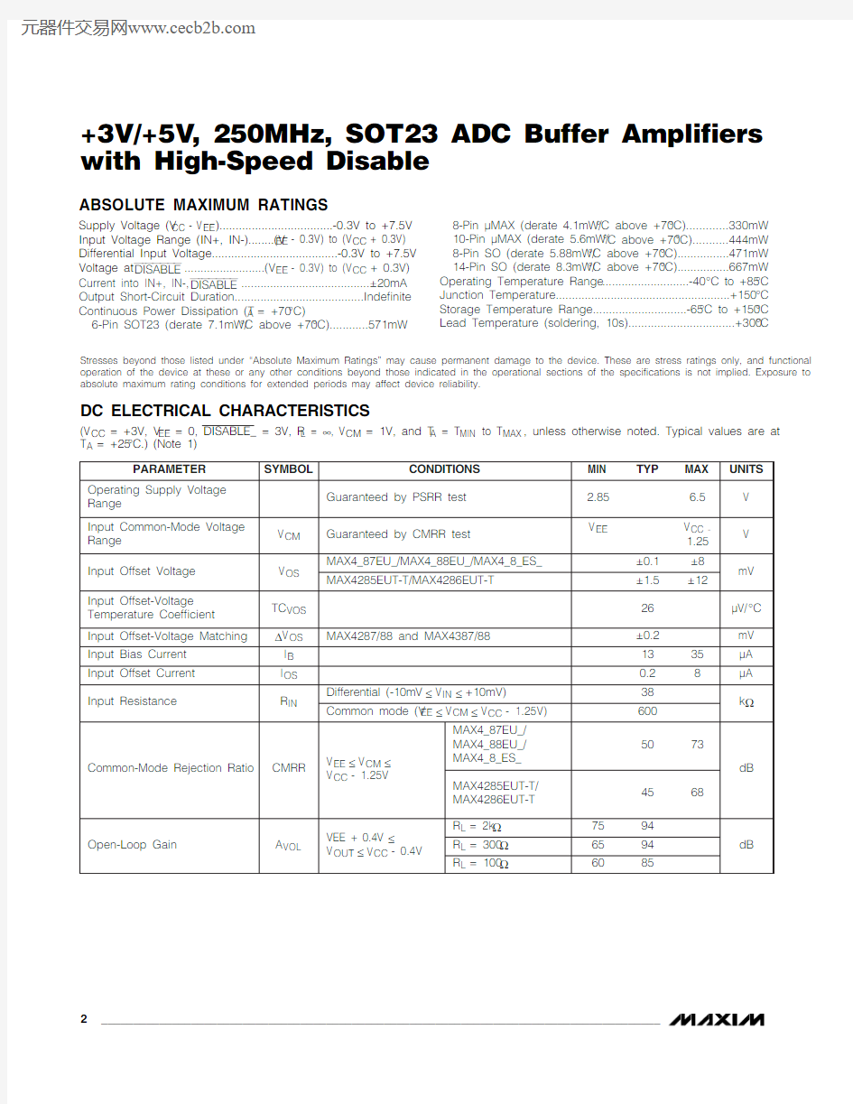
ABSOLUTE MAXIMUM RATINGS
DC ELECTRICAL CHARACTERISTICS
Stresses beyond those listed under “Absolute Maximum Ratings” may cause permanent damage to the device. These are stress ratings only, and functional operation of the device at these or any other conditions beyond those indicated in the operational sections of the specifications is not implied. Exposure to absolute maximum rating conditions for extended periods may affect device reliability.
Supply Voltage (V CC - V EE )...................................-0.3V to +7.5V Input Voltage Range (IN+, IN-)........(V EE - 0.3V) to (V CC + 0.3V) Differential Input Voltage.......................................-0.3V to +7.5V Voltage at DISABLE .........................(V EE - 0.3V) to (V CC + 0.3V)Current into IN+, IN-, DISABLE ........................................±20mA Output Short-Circuit Duration........................................Indefinite Continuous Power Dissipation (T A = +70°C)
6-Pin SOT23 (derate 7.1mW/°C above +70°C)............571mW
8-Pin μMAX (derate 4.1mW/°C above +70°C).............330mW 10-Pin μMAX (derate 5.6mW/°C above +70°C)...........444mW 8-Pin SO (derate 5.88mW/°C above +70°C)................471mW 14-Pin SO (derate 8.3mW/°C above +70°C)................667mW Operating Temperature Range ...........................-40°C to +85°C Junction Temperature......................................................+150°C Storage Temperature Range.............................-65°C to +150°C Lead Temperature (soldering, 10s).................................+300°C
MAX4285–MAX4288/MAX4387/MAX4388
+3V/+5V , 250MHz, SOT23 ADC Buffer Amplifiers
with High-Speed Disable
_______________________________________________________________________________________3
DC ELECTRICAL CHARACTERISTICS (continued)
M A X 4285–M A X 4288/M A X 4387/M A X 4388
+3V/+5V , 250MHz, SOT23 ADC Buffer Amplifiers with High-Speed Disable 4_______________________________________________________________________________________
AC ELECTRICAL CHARACTERISTICS
(V CC = +3V, V EE = 3V, R L = 300?to V CC /2, V CM = 1V, A VCL = +1V/V for MAX4285/MAX4287/MAX4288, A VCL =+5V/V for MAX4286 and MAX4387/MAX4388, T A = +25°C, unless otherwise noted.)
MAX4285–MAX4288/MAX4387/MAX4388
+3V/+5V , 250MHz, SOT23 ADC Buffer Amplifiers
with High-Speed Disable
_______________________________________________________________________________________5
AC ELECTRICAL CHARACTERISTICS (continued)
(V CC = +5V, V EE = 5V, R L = 300?to V CC /2, V CM = 2.5V, A VCL = +1V/V for MAX4285/MAX4287/MAX4288, A VCL =+5V/V for MAX4286 and MAX4387/MAX4388, T A = +25°C, unless otherwise noted.)
Note 1:The MAX428_EUT (SOT23) are 100% production tested at T A = +25°C. Specifications over temperature limits are guaran-teed by design.
M A X 4285–M A X 4288/M A X 4387/M A X 4388
+3V/+5V , 250MHz, SOT23 ADC Buffer Amplifiers with High-Speed Disable 6_______________________________________________________________________________________
100M
1G
-6-3-4-5-2-102134100k
1M
10M MAX4285/MAX4287/MAX4288SMALL-SIGNAL GAIN vs. FREQUENCY
FREQUENCY (Hz)
G A I N (d B )
100M 1G
-6-3-4-5-2-102134100k
1M 10M MAX4286/MAX4387/MAX4388
SMALL-SIGNAL GAIN vs. FREQUENCY
FREQUENCY (Hz)
G A I N (d B )
100M 1G
-0.5-0.2-0.3-0.4-0.100.10.30.20.40.5
100k
1M 10M MAX4285/MAX4387/MAX4288GAIN FLATNESS vs. FREQUENCY
(R LOAD = 100?)
FREQUENCY (Hz)
G A I N (d B )
100M
1G
-0.6-0.3-0.4-0.5-0.2-0.100.20.10.30.4100k
1M
10M MAX4285/MAX4287/MAX4288GAIN FLATNESS vs. FREQUENCY
(R LOAD = 300?
)
FREQUENCY (Hz)
G A I N (d B )
100M
1G
-6-3-4-5-2-102134100k
1M
10M LARGE-SIGNAL GAIN vs. FREQUENCY
M A 4285-07
FREQUENCY (Hz)
G A I N (d B )
100M 1G -0.5-0.2-0.3-0.4-0.100.10.30.20.40.5100k
1M 10M MAX4285/MAX4287/MAX4288GAIN FLATNESS vs. FREQUENCY
(R LOAD = 1k ?
)
FREQUENCY (Hz)
G A I N (d B )
100M 1G
-0.6-0.3-0.4-0.5-0.2-0.100.20.10.30.4
100k
1M 10M MAX4286/MAX4387/MAX4388GAIN FLATNESS vs. FREQUENCY
FREQUENCY (Hz)
G A I N (d B )
0.1
1
10
100
MAX4285/MAX4287/MAX4288DISTORTION vs. FREQUENCY
FREQUENCY (MHz)
G A I N (d B )
-40-100
-90
-80
-70-60-500.11
10
100
MAX4286/MAX4387/MAX4388DISTORTION vs. FREQUENCY
FREQUENCY (MHz)
G A I N (d B )
-40-100
-90
-80
-70-60-50Typical Operating Characteristics
(V CC = +3V, V EE = 0, DISABLE_ ≥2V, R L = 300?to V CC /2, V CM = +1.0V, T A =+25°C, unless otherwise noted.)
MAX4285–MAX4288/MAX4387/MAX4388
+3V/+5V , 250MHz, SOT23 ADC Buffer Amplifiers
with High-Speed Disable
_______________________________________________________________________________________7
Typical Operating Characteristics (continued)
(V CC = +3V, V EE = 0, DISABLE_ ≥2V, R L = 300?to V CC /2, V CM = +1.0V, T A =+25°C, unless otherwise noted.)
-120
-100-110-70-80-90-50-60-401004005002003006007008009001000
MAX4285/MAX4287/MAX4288
DISTORTION vs. LOAD
RESISTIVE LOAD (?)
D I S T O R T I O N (d B c )
-120
-100-110-70-80-90-50-60-40100400500200300600700800900
1000
MAX4286/MAX4387/MAX4388
DISTORTION vs. LOAD
RESISTIVE LOAD (?)
D I S T O R T I O N (d B c )
-120
-110-100-90-80-70-60-50-40
0.25
0.50
0.75
1.00
1.25
MAX4285/MAX4287/MAX4288
DISTORTION vs. SWING
VOLTAGE (Vp-p)
D I S T O R T I O N (d B c )
-120
-110-100-90-80-70-60-50-400
0.250.500.75 1.00 1.25
MAX4286/MAX4387/MAX4388
DISTORTION vs. SWING
VOLTAGE (Vp-p)
D I S T O R T I O N (d B c )
100M 1G -120
-60-80-100-40-20040206080100k
1M 10M MAX4285/MAX4286/MAX4288/MAX4388
OFF-ISOLATION vs. FREQUENCY
M A 4285-15
FREQUENCY (Hz)
O F F -I S O L A T I O N
80
-120
0.11101001000
MAX4287/MAX4288/MAX4387/MAX4388
CROSSTALK vs. FREQUENCY
-80M A X 4285-16
FREQUENCY (MHz)
G A I N (d B )
-4004020-20-60-10060INPUT 500mV/
div OUTPUT 500mV/
div
MAX4285/MAX4287/MAX4288LARGE-SIGNAL PULSE RESPONSE
(A V = +1V/V)
M A 4285-17
V O L T A G E (V ) TIME (5ns/div)
INPUT 100mV/
div OUTPUT 500mV/
div
TIME (5ns/div)
MAX4286/MAX4387/MAX4388LARGE-SIGNAL PULSE RESPONSE
(A V = +5V/V)
M A 4285-18
V O L T A G E (V )
M A X 4285–M A X 4288/M A X 4387/M A X 4388
+3V/+5V , 250MHz, SOT23 ADC Buffer Amplifiers with High-Speed Disable 8_______________________________________________________________________________________
INPUT 50mV/div OUTPUT 50mV/div
MAX4285/MAX4287/MAX4288SMALL-SIGNAL PULSE RESPONSE
(A V = +1V/V)
M A 4285-19
V O L T A G E (V )
TIME (5ns/div)
INPUT 10mV/div OUTPUT 50mV/div
TIME (5ns/div)
MAX4286/MAX4387/MAX4388SMALL-SIGNAL PULSE RESPONSE
(A V = +5V/V)
M A 4285-20
V O L T A G E (V )
INPUT 50mV/div
OUTPUT 50mV/div
MAX4285/MAX4287/MAX4288SMALL-SIGNAL PULSE RESPONSE (C LOAD = 22pF, A V = +1V/V)
M A 4285-21
V O L T A G E (V )
TIME (5ns/div)
INPUT 10mV/div OUTPUT 50mV/div
TIME (5ns/div)
MAX4286/MAX4387/MAX4388SMALL-SIGNAL PULSE RESPONSE (C LOAD = 47pF, A V = +5V/V)
M A 4285-22
V O L T A G E (V )
100M 1G
-60-50-40-20-30-100100k
1M 10M POWER-SUPPLY REJECTION RATIO
vs. FREQUENCY
M A 4285-27
FREQUENCY (Hz)
P S R R (d B )
10
141218162220244010013070160190220250ISOLATION RESISTANCE vs. LOAD CAPACITANCE
C LOA
D (pF)
R I S O (?)
100M 1G
00.60.40.20.81.01.21.61.41.82.0
100k
1M 10M GROUP DELAY vs. FREQUENCY
M A 4285-26
FREQUENCY (Hz)
T I M E (n s )
100M
1G
-100
-70-80-90-60-50-40-20-30-100100k
1M
10M COMMON-MODE REJECTION
vs. FREQUENCY
M A 4285-28
FREQUENCY (Hz)
C M R (d B )
10k
100k
1M
10M
100M
1G
OUTPUT IMPEDANCE vs. FREQUENCY
M A X 4285-29
FREQUENCY (Hz)
I M P E D A N C E (?)
100
0.01
0.1
1
10Typical Operating Characteristics (continued)
(V CC = +3V, V EE = 0, DISABLE_ ≥2V, R L = 300?to V CC /2, V CM = +1.0V, T A =+25°C, unless otherwise noted.)
MAX4285–MAX4288/MAX4387/MAX4388
+3V/+5V , 250MHz, SOT23 ADC Buffer Amplifiers
with High-Speed Disable
_______________________________________________________________________________________9
Typical Operating Characteristics (continued)
(V CC = +3V, V EE = 0, DISABLE_ ≥2V, R L = 300?to V CC /2, V CM = +1.0V, T A =+25°C, unless otherwise noted.)
VOLTAGE NOISE DENSITY
vs. FREQUENCY
M A X 4285-30
FREQUENCY (Hz)
V O L T A G E N O I S E (n v /H z )
100
11010
10k
100k
1M
100
1k
10M
100
1
1
10k
100k
1M
100
1k
10M
CURRENT NOISE DENSITY
vs. FREQUENCY
10
M A X 4285-31
FREQUENCY (Hz)
N O I S E (p A /√H z )
10
10
1211
1413161517191820
-50-20-510-352540558570100
INPUT BIAS CURRENT vs. TEMPERATURE
M A X 4285-32
TEMPERATURE (°C)
I N P U T B I A S C U R R E N T (μA )
0.1
0.2
0.3
0.4
0.5
-501025-20-5-3540557085100
INPUT OFFSET CURRENT vs. TEMPERATURE
TEMPERATURE (°C)
I N P U T O F F S E T C U R R E N T (μ
A )
100M
1G
-10-4-6-8-20264810100k
1M
10M MAX4286
SMALL-SIGNAL GAIN vs. FREQUENCY
(C LOAD = 22pF)
FREQUENCY (Hz)
G A I N (d B )
-5
-3-4
-1-2102435
-50-20-510-352540558570100
INPUT OFFSET VOLTAGE vs. TEMPERATURE
M A X 4285-34
TEMPERATURE (°C)
I N P U T O F F S E T V O L T A G E (m V )
18
19
21
20
22-50-20-51025-3540557085100
POWER-SUPPLY CURRENT vs. TEMPERATURE
M A X 4285-35
TEMPERATURE (°C)
P O W E R -S U P P L Y C U R R E N T
(m A )
100M 1G -10-4-6-8-20264810100k
1M 10M MAX4286
SMALL-SIGNAL GAIN vs. FREQUENCY
(C LOAD = 37pF)
FREQUENCY (Hz)
G A I N (d B
)
100M 1G
-10-4-6-8-20264810
100k
1M 10M MAX4286
SMALL-SIGNAL GAIN vs. FREQUENCY
(C LOAD = 47pF)
FREQUENCY (Hz)
G A I N (d B )
M A X 4285–M A X 4288/M A X 4387/M A X 4388
+3V/+5V , 250MHz, SOT23 ADC Buffer Amplifiers with High-Speed Disable 10______________________________________________________________________________________
100M
1G
-2.5-1.0-1.5-2.0-0.500.51.51.02.02.5100k
1M
10M MAX4286
SMALL-SIGNAL GAIN vs. FREQUENCY
C LOA
D || R ISO (C LOAD = 37pF)
FREQUENCY (Hz)
G A I N (d B )
100M 1G -2.5-1.0-1.5-2.0-0.500.51.51.02.02.5100k
1M 10M MAX4286
SMALL-SIGNAL GAIN vs. FREQUENCY
C LOA
D || R ISO (C LOAD = 37pF)
FREQUENCY (Hz)
G A I N (d B )
100M 1G
-2.5-1.0-1.5-2.0-0.500.51.51.02.02.5
100k
1M 10M MAX4286
SMALL-SIGNAL GAIN vs. FREQUENCY
C LOA
D || R ISO (C LOAD = 37pF)
FREQUENCY (Hz)
G A I N (d B )
V CC - 1V
TIME (20ns/div)ENABLE/DISABLE RESPONSE
TIME (V CC = 5V)
M A 4285-45
V EE + 1V V CC - 1V
TIME (20ns/div)
ENABLE/DISABLE RESPONSE
TIME (V CC = 3V)
M A 4285-46
V EE + 1V
Typical Operating Characteristics (continued)
(V CC = +3V, V EE ≥2V, R L = 300?to V CC /2, V CM = +1.0V, T A =+25°C, unless otherwise noted.)
MAX4285–MAX4288/MAX4387/MAX4388
+3V/+5V , 250MHz, SOT23 ADC Buffer Amplifiers
with High-Speed Disable
______________________________________________________________________________________
11
Pin Description
Detailed Description
The MAX4285–MAX4288 and MAX4387/MAX4388 are voltage-feedback op amps, intended for use as ADC input buffers. They operate from a single +2.85V to +6.5V supply or dual ±1.425V to ±3.25V supplies. Their high output drive, wide bandwidth, fast settling, low noise, and low distortion make them ideal for the brutal task of meeting the dynamic input drive requirements of high-speed ADCs or other demanding applications.The MAX4285/MAX4286/MAX4288 and MAX4388 have a high-speed disable mode that places the outputs in a high-impedance state and lowers operating supply cur-rent to 1mA. The enable time is typically 40ns, and the disable time is typically 50ns. The MAX4285/MAX4286have a single enable pin (DISABLE), and the MAX4288/
MAX4388 have dual disable pins (DI The MAX4285/MAX4287/MAX4288 are internally com-pensated for unity-gain stability. The MAX4286/MAX4387/MAX4388 are compensated for gains of +5V/V or greater.
Applications Information
Inverting and Noninverting Configurations
Select the gain-setting feedback (R F ) and input (R G )resistor values considering the following criteria: large resistor values increase voltage noise and interact with the amplifier ’s input and PC board capacitance to effect system bandwidth. This generates undesirable poles and zeros that decrease bandwidth or cause oscillations.
M A X 4285–M A X 4288/M A X 4387/M A X 4388
+3V/+5V , 250MHz, SOT23 ADC Buffer Amplifiers with High-Speed Disable 12______________________________________________________________________________________
S Loads
For example, a noninverting gain-of-two configuration (R F = R G ) using 1k ?resistors, combined with 2pF typi-cal amplifier input capacitance, generates a pole at 159MHz. Since this pole is within the amplifier band-width, it jeopardizes stability. Reducing these 1k ?resistors to 100?extends the pole frequency to 1.59GHz, but affects output swing by adding 200?in parallel with the amplifier ’s load resistor. The typical value for R F is 300?.
Layout and Power-Supply Bypassing
These amplifiers operate from a single +2.85V to +6.5V power supply or from ±1.425V to ±3.25V dual supplies.For single-supply operation, bypass V CC to ground with a 0.1nF capacitor as close to the pin as possible, with a 0.1μF capacitor in parallel. I f operating with dual sup-plies, bypass each supply with capacitors to ground. Observe the following guidelines:? A solid ground plane is essential for good high-fre-quency behavior.
?Where possible, use multiple ground vias.
?Use a PC board with at least two layers. Avoid areas of unreferenced copper-clad.
?
Keep signal traces as short and as straight as pos-sible. Do not make sharp turns; round all trace corners.
?
Use a constant-impedance board design if possi-ble.
High-Speed Disable
The MAX4285/MAX4286/MAX4288 and MAX4388 fea-ture a disable (DISABLE_) input that places the amplifi-er in a low-power, high-output-impedance state.When DISABLE_is asserted, the amplifier ’s output impedance is typically 35k ?. This high output impedance, com-bined with the low 2pF output capacitance, make these devices ideal for ADC input multiplexing applications or switch applications. Typical enable/disable times are 40ns/50ns.
Output Capacitive Loading and Stability
These op amps are optimized for AC performance.They are not designed to drive highly reactive loads,which decrease phase margin and may produce excessive ringing and oscillation. A small isolation resistor (usually 20?to 30?) placed before the reactive load reduces possible ringing and oscillation (Figure 1). At higher capacitive loads, AC performance is dependent on the interaction of the load capacitance,the isolation resistor, and on-board layout.
Output Drive Capability
The MAX4285–MAX4288 and MAX4387/MAX4388 have an output sink capability of 106mA and a source capa-bility of 77mA. This high current ability allows them to drive low-impedance and dynamic-impedance ADC inputs. The linear output range of these devices is (V EE + 0.4V) to (V CC - 0.4V). Operation beyond this range is not recommended due to reduced gain and phase margin.
MAX4285–MAX4288/MAX4387/MAX4388
+3V/+5V , 250MHz, SOT23 ADC Buffer Amplifiers
with High-Speed Disable
Ordering Information (continued)
Typical Operating Circuit
Chip Information
TRANSISTOR COUNT:MAX4285/MAX4286 : 114
MA4287/MAX4288/
MAX4387/MAX4388 : 227
Pin Configurations
M A X 4285–M A X 4288/M A X 4387/M A X 4388
+3V/+5V , 250MHz, SOT23 ADC Buffer Amplifiers with High-Speed Disable 14______________________________________________________________________________________
Package Information
MAX4285–MAX4288/MAX4387/MAX4388
+3V/+5V , 250MHz, SOT23 ADC Buffer Amplifiers
with High-Speed Disable
______________________________________________________________________________________15
Package Information (continued)
M A X 4285–M A X 4288/M A X 4387/M A X 4388
+3V/+5V , 250MHz, SOT23 ADC Buffer Amplifiers with High-Speed Disable Maxim cannot assume responsibility f or use of any circuitry other than circuitry entirely embodied in a Maxim product. No circuit patent licenses are implied. Maxim reserves the right to change the circuitry and specifications without notice at any time.
16____________________Maxim Integrated Products, 120 San Gabriel Drive, Sunnyvale, CA 94086 408-737-7600?2000 Maxim Integrated Products
Printed USA
is a registered trademark of Maxim Integrated Products.
Package Information (continued)