ANPEC reserves the right to make changes to improve reliability or manufacturability without notice, and advise customers to obtain the latest version of relevant information to verify before placing orders.APM9935K
Features
Applications
? -20V/-6A ,
R DS(ON)=30m ?(typ.) @ V GS =-4.5V R DS(ON)=38m ?(typ.) @ V GS =-2.5V
? Super High Dense Cell Design ? Reliable and Rugged
? Lead Free Available (RoHS Compliant)
? Power Management in Notebook Computer,
Portable Equipment and Battery Powered Systems
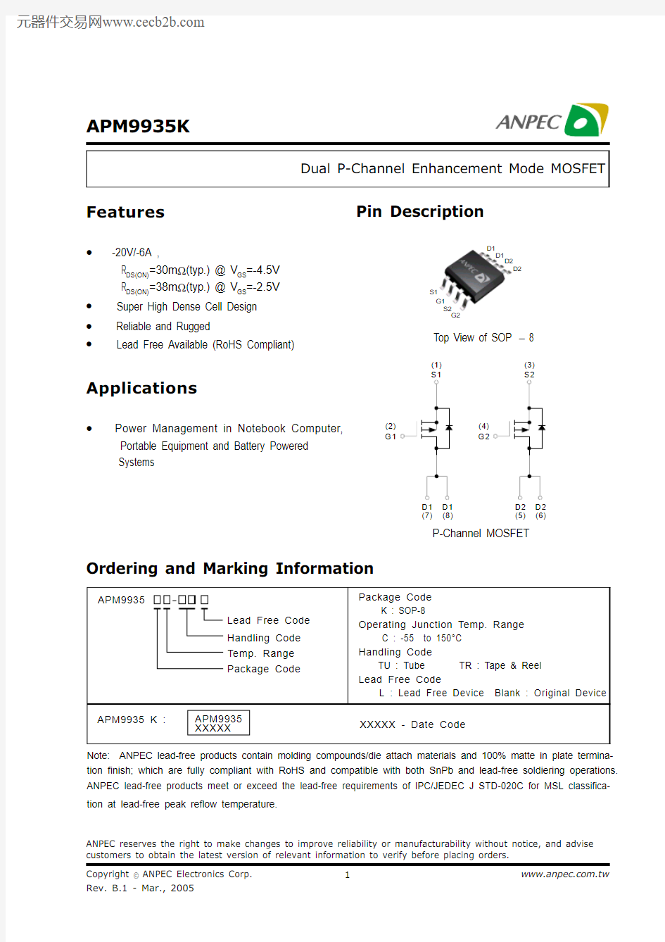
Pin Description
Ordering and Marking Information
P-Channel MOSFET
APM9935
Handling Code Temp. Range Package Code
Package Code K : SOP-8
Operating Junction Temp. Range C : -55 to 150°C Handling Code
TU : Tube TR : Tape & Reel Lead Free Code
L : Lead Free Device Blank : Original Device APM9935 K :
APM9935XXXXX
XXXXX - Date Code
Lead Free Code G1S1S2G2
D1D1D2D2
Top View of SOP
? 8
D2G2
D2(4)(3)(5)
(6)
D1G1
D1(2)(1)(7)(8)Note: ANPEC lead-free products contain molding compounds/die attach materials and 100% matte in plate termina-tion finish; which are fully compliant with RoHS and compatible with both SnPb and lead-free soldiering operations.ANPEC lead-free products meet or exceed the lead-free requirements of IPC/JEDEC J STD-020C for MSL classifica-tion at lead-free peak reflow temperature.
APM9935K
Absolute Maximum Ratings (T A = 25°C unless otherwise noted)
*Surface Mounted on 1in2 pad area, t ≤ 10sec.
Electrical Characteristics (T A = 25°C unless otherwise noted)
APM9935K
Electrical Characteristics (Cont.) (T A = 25°C unless otherwise noted)
a : Pulse test ; pulse width≤300μs, duty cycle≤2%.
b : Guaranteed by design, not subject to production testing.
APM9935K
1E-4
1E-30.010.111030
1E-30.01
0.1
1
2
Typical Characteristics
-I D - D r a i n C u r r e n t (A )
Drain Current
T j - Junction Temperature (°C)
Safe Operation Area
-V DS - Drain - Source Voltage (V)Thermal Transient Impedance
Square Wave Pulse Duration (sec)
Power Dissipation
P t o t - P o w e r (W )
T j - Junction T emperature (°C)
-I D - D r a i n C u r r e n t (A )
20
40
60
80100120140160
0.0
0.5
1.0
1.5
2.0
2.5
20
40
60
80
100120
140160
2
4
6
8
0.01
0.1
1
10100
0.010.11
10
50
N o r m a l i z e d T r a n s i e
n t T h e r m a l R e s i s t a n c e
APM9935K
R D S (O N ) - O n - R e s i s t a n c e (m ?)
Drain-Source On Resistance
-I D - Drain Current (A)
T j - Junction T emperature (°C)
Gate Threshold Voltage
N o r m a l i z e d T h r e s h o l d V l o t a g e
-V DS - Drain - Source Voltage (V)-I D - D r a i n C u r r e n t (A )
Transfer Characteristics
-V GS - Gate - Source Voltage (V)
-I D - D r a i n C u r r e n t (A )
Typical Characteristics (Cont.)
246810121416
1820
10
15
2025303540
455055
60
0.0
0.5
1.0 1.5
2.0 2.5
3.00246810
121416
1820
-50
-250255075100125
0.00
0.250.500.751.001.251.501.75
2.00
APM9935K
Typical Characteristics (Cont.)
Drain-Source On Resistance Source-Drain Diode Forward
APM9935K
Packaging Information
SOP-8 pin ( Reference JEDEC Registration MS-012)
APM9935K
T L
T P
25
T e m p e r a t u r e
Tim e
Reflow Condition (IR/Convection or VPR Reflow)
Classification Reflow Profiles
Physical Specifications
APM9935K
Classification Reflow Profiles(Cont.)
Reliability Test Program
Carrier Tape & Reel Dimensions
APM9935K
Customer Service
Anpec Electronics Corp.Head Office :
5F, No. 2 Li-Hsin Road, SBIP,Hsin-Chu, T aiwan, R.O.C.T el : 886-3-5642000Fax : 886-3-5642050Taipei Branch :
7F, No. 137, Lane 235, Pac Chiao Rd.,
Hsin Tien City, Taipei Hsien, T aiwan, R. O. C.T el : 886-2-89191368Fax : 886-2-89191369
Cover Tape Dimensions
Carrier Tape & Reel Dimensions(Cont.)
(mm)