General Description
The MAX6956 compact, serial-interfaced LED display driver/I/O expander provide microprocessors with up to 28 ports. Each port is individually user configurable to either a logic input, logic output, or common-anode (CA) LED constant-current segment driver. Each port configured as an LED segment driver behaves as a digitally controlled constant-current sink, with 16 equal current steps from 1.5mA to 24mA. The LED drivers are suitable for both discrete LEDs and CA numeric and alphanumeric LED digits.
Each port configured as a general-purpose I/O (GPIO)can be either a push-pull logic output capable of sink-ing 10mA and sourcing 4.5mA, or a Schmitt logic input with optional internal pullup. Seven ports feature config-urable transition detection logic, which generates an interrupt upon change of port logic level. The MAX6956is controlled through an I 2C-compatible 2-wire serial interface, and uses four-level logic to allow 16 I 2C addresses from only 2 select pins.
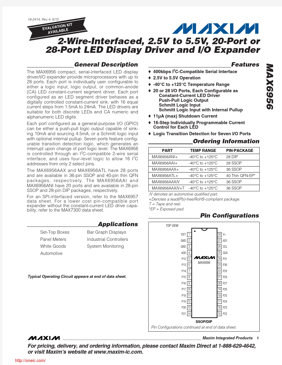
The MAX6956AAX and MAX6956ATL have 28 ports and are available in 36-pin SSOP and 40-pin thin QFN packages, respectively. The MAX6956AAI and MAX6956ANI have 20 ports and are available in 28-pin SSOP and 28-pin DIP packages, respectively.
For an SPI-interfaced version, refer to the MAX6957data sheet. For a lower cost pin-compatible port expander without the constant-current LED drive capa-bility, refer to the MAX7300 data sheet.
Applications
Set-Top Boxes Bar Graph Displays Panel Meters Industrial Controllers White Goods System Monitoring
Automotive
Features
o 400kbps I 2C-Compatible Serial Interface o 2.5V to 5.5V Operation
o -40°C to +125°C Temperature Range o
20 or 28 I/O Ports, Each Configurable as Constant-Current LED Driver Push-Pull Logic Output Schmitt Logic Input
Schmitt Logic Input with Internal Pullup o 11μA (max) Shutdown Current
o 16-Step Individually Programmable Current Control for Each LED
o Logic Transition Detection for Seven I/O Ports
MAX6956
, 20-Port or 28-Port LED Display Driver and I/O Expander
________________________________________________________________Maxim Integrated Products
1
Pin Configurations
For pricing, delivery, and ordering information,please contact Maxim Direct at 1-888-629-4642,or visit Maxim’s website at https://www.doczj.com/doc/a715018894.html,.
Typical Operating Circuit appears at end of data sheet.
Ordering Information
/V denotes an automotive qualified part.
+Denotes a lead(Pb)-free/RoHS-compliant package.T = Tape and reel.*EP = Exposed pad.
M A X 6956
2-Wire-Interfaced, 2.5V to 5.5V , 20-Port or 28-Port LED Display Driver and I/O Expander
ABSOLUTE MAXIMUM RATINGS
Stresses beyond those listed under “Absolute Maximum Ratings” may cause permanent damage to the device. These are stress ratings only, and functional operation of the device at these or any other conditions beyond those indicated in the operational sections of the specifications is not implied. Exposure to absolute maximum rating conditions for extended periods may affect device reliability.
Voltage (with Respect to GND)
V+.............................................................................-0.3V to +6V SCL, SDA, AD0, AD1................................................-0.3V to +6V All Other Pins................................................-0.3V to (V+ + 0.3V)P4–P31 Current ................................................................±30mA GND Current.....................................................................800mA Continuous Power Dissipation
28-Pin PDIP (derate 14.3mW/°C above T A = +70°C)1143mW 28-Pin SSOP (derate 9.1mW/°C above T A = +70°C)...727mW
36-Pin SSOP (derate 11.8mW/°C above T A = +70°C)...941mW 40-Pin TQFN (derate 26.3mW/°C above T A = +70°C) 2105mW Operating Temperature Range
(T MIN to T MAX )...............................................-40°C to +125°C Junction Temperature......................................................+150°C Storage Temperature Range.............................-65°C to +150°C Soldering Temperature (reflow)
Lead(Pb)-free packages...............................................+260°C Packages containing lead(Pb)......................................+240°C
ELECTRICAL CHARACTERISTICS
MAX6956
2-Wire-Interfaced, 2.5V to 5.5V , 20-Port or 28-Port LED Display Driver and I/O Expander
_______________________________________________________________________________________3
A Note 2:Guaranteed by design.
Note 3:A master device must provide a hold time of at least 300ns for the SDA signal (referred to V IL of the SCL signal) in order to
bridge the undefined region of SCL’s falling edge.
Note 4:C b = total capacitance of one bus line in pF. t R and t F measured between 0.3V+ and 0.7V+.
Note 5:I SINK ≤6mA. C b = total capacitance of one bus line in pF. t R and t F measured between 0.3V+ and 0.7V+. Note 6:Input filters on the SDA and SCL inputs suppress noise spikes less than 50ns.
ELECTRICAL CHARACTERISTICS (continued)
(Typical Operating Circuit , V+ = 2.5V to 5.5V, T A = T MIN to T MAX , unless otherwise noted.) (Note 1)
M A X 6956
2-Wire-Interfaced, 2.5V to 5.5V , 20-Port or 28-Port LED Display Driver and I/O Expander 4_______________________________________________________________________________________
OPERATING SUPPLY CURRENT
vs. TEMPERATURE
TEMPERATURE (°C)
S U P P L Y C U R R E N T (m A )
97.5
70.0
42.5
15.0
-12.5
0.040.080.120.160.200.240.280.320.360.400
-40.0
125.0
SHUTDOWN SUPPLY CURRENT
vs. TEMPERATURE
TEMPERATURE (°C)
S U P P L Y C U R R E N T (μA )
97.5
70.0
42.5
15.0
-12.5
4
56
78
3
-40.0
125.0
OPERATING SUPPLY CURRENT vs. V+
(NO LOADS)
V+ (V)
S U P P L Y C U R R E N T (m A )
5.0
4.5
4.0
3.5
3.0
2.5
0.1
1
10
100
0.01
2.0
5.5
LED DRIVER SINK CURRENT
vs. V+
V+ (V)P O R T S I N K C U R R E N T (m A )
5.0
4.5
3.5
4.0
3.0
2.5
810121416182022242662.0
5.5GPO SOURCE CURRENT vs. TEMPERATURE
(OUTPUT = 1)
TEMPERATURE (°C)
P O R T S O U R C E C U R R E N T (m A
)
97.5
70.0
42.5
15.0
-12.5
3456789
2-40.0
125.0
LED DRIVER SINK CURRENT
vs. TEMPERATURE
TEMPERATURE (
°C)P O R T S I N K C U R R E N T (m A )
97.570.042.515.0-12.5212223
2425262720
-40.0125.0GPO SINK CURRENT vs. TEMPERATURE
(OUTPUT = 0)
TEMPERATURE (°C)
P O R T S I N K C U R R E N T (m A )
97.570.0-12.515.042.54681012141618
2
-40.0125.0
GPI PULLUP CURRENT vs. TEMPERATURE
TEMPERATURE (°C)
P U L L U P C U R R E N T (μA )
97.5
70.0
42.5
15.0
-12.5
100
100010
-40.0
125.0
GPO SHORT-CIRCUIT CURRENT
vs. TEMPERATURE
TEMPERATURE (°C)
P O R T C U R R E N T (m A )
97.5
70.0
42.5
15.0
-12.5
10
100
1-40.0
125.0
__________________________________________Typical Operating Characteristics
(R ISET = 39k ?, T A = +25°C, unless otherwise noted.)
Detailed Description The MAX6956 LED driver/G PIO peripheral provides up to 28 I/O ports, P4 to P31, controlled through an I2C-com-patible serial interface. The ports can be configured to any combination of constant-current LED drivers, logic inputs and logic outputs, and default to logic inputs on power-up. When fully configured as an LED driver, the MAX6956 controls up to 28 LED segments with individual 16-step adjustment of the constant current through each LED segment. A single resistor sets the maximum seg-ment current for all segments, with a maximum of 24mA per segment. The MAX6956 drives any combination of discrete LEDs and CA digits, including seven-segment and starburst alphanumeric types.
Figure 1 is the MAX6956 functional diagram. Any I/O port can be configured as a push-pull output (sinking 10mA, sourcing 4.5mA), or a Schmitt-trigger logic input. Each input has an individually selectable internal pullup resistor. Additionally, transition detection allows seven ports (P24 through P30) to be monitored in any mask-able combination for changes in their logic status. A detected transition is flagged through a status register bit, as well as an interrupt pin (port P31), if desired. The Typical Operating Circuit shows two MAX6956s working together controlling three monocolor 16-seg-GPIO (P26–P31 of U2).
The port configuration registers set the 28 ports, P4 to
P31, individually as either LED drivers or GPIO. A pair
of bits in registers 0x09 through 0x0F sets each port’s configuration (Tables 1 and 2).
The 36-pin MAX6956AAX has 28 ports, P4 to P31. The
28-pin MAX6956ANI and MAX6956AAI make only 20
ports available, P12 to P31. The eight unused ports should be configured as outputs on power-up by writ-
ing 0x55 to registers 0x09 and 0x0A. If this is not done,
the eight unused ports remain as unconnected inputs
and quiescent supply current rises, although there is no damage to the part.
Register Control of I/O Ports and LEDs
Across Multiple Drivers
The MAX6956 offers 20 or 28 I/O ports, depending on package choice. These can be applied to a variety of combinations of different display types, for example: seven, 7-segment digits (Figure 7). This example requires two MAX6956s, with one digit being driven by
both devices, half by one MAX6956, half by the other (digit 4 in this example). The two drivers are static, and therefore do not need to be synchronized. The
MAX6956 sees CA digits as multiple discrete LEDs. To
MAX6956
2-Wire-Interfaced, 2.5V to 5.5V, 20-Port or 28-Port LED Display Driver and I/O Expander
_______________________________________________________________________________________5
M A X 6956
simplify access to displays that overlap two MAX6956s,the MAX6956 provides four virtual ports, P0 through P3.To update an overlapping digit, send the same code twice as an eight-port write, once to P28 through P35 of the first driver, and again to P0 through P7 of the sec-ond driver. The first driver ignores the last 4 bits and the second driver ignores the first 4 bits.
Two addressing methods are available. Any single port (bit) can be written (set/cleared) at once; or, any sequence of eight ports can be written (set/cleared) in any combination at once. There are no boundaries; it is equally acceptable to write P0 through P7, P1 through P8, or P31 through P38 (P32 through P38 are nonexis-tent, so the instructions to these bits are ignored).
Using 8-bit control, a seven-segment digit with a deci-mal point can be updated in a single byte-write, a 14-segment digit with DP can be updated in two byte-writes, and 16-segment digits with DP can be updated in two byte-writes plus a bit write. Also, discrete LEDs and GPIO port bits can be lit and controlled individually without affecting other ports.
Shutdown
When the MAX6956 is in shutdown mode, all ports are forced to inputs (which an be read), and the pullup cur-rent sources are turned off. Data in the port and control registers remain unaltered, so port configuration and output levels are restored when the MAX6956 is taken out of shutdown. The display driver can still be pro-grammed while in shutdown mode. For minimum sup-ply current in shutdown mode, logic inputs should be at GND or V+ potential. Shutdown mode is exited by set-ting the S bit in the configuration register (Table 8).
2-Wire-Interfaced, 2.5V to 5.5V , 20-Port or 28-Port LED Display Driver and I/O Expander 6
_______________________________________________________________________________________
Shutdown mode is temporarily overridden by the dis-play test function.
Serial Interface
Serial Addressing
The MAX6956 operates as a slave that sends and receives data through an I 2C-compatible 2-wire inter-face. The interface uses a serial data line (SDA) and a serial clock line (SCL) to achieve bidirectional commu-nication between master(s) and slave(s). A master (typ-ically a microcontroller) initiates all data transfers to and from the MAX6956, and generates the SCL clock that synchronizes the data transfer (Figure 2).
The MAX6956 SDA line operates as both an input and an open-drain output. A pullup resistor, typically 4.7k ?,
is required on SDA. The MAX6956 SCL line operates only as an input. A pullup resistor, typically 4.7k ?, is required on SCL if there are multiple masters on the 2-wire interface, or if the master in a single-master system has an open-drain SCL output.
Each transmission consists of a START condition (Figure 3) sent by a master, followed by the MAX69567-bit slave address plus R/W bit (Figure 6), a register address byte, one or more data bytes, and finally a STOP condition (Figure 3).
Start and Stop Conditions
Both SCL and SDA remain high when the interface is not busy. A master signals the beginning of a transmis-sion with a START (S) condition by transitioning SDA from high to low while SCL is high. When the master
MAX6956
2-Wire-Interfaced, 2.5V to 5.5V , 20-Port or 28-Port LED Display Driver and I/O Expander
_______________________________________________________________________________________________________
7
Figure 1. MAX6956 Functional Diagram
M A X 6956
has finished communicating with the slave, it issues a STOP (P) condition by transitioning SDA from low to high while SCL is high. The bus is then free for another transmission (Figure 3).
Bit Transfer
One data bit is transferred during each clock pulse.The data on SDA must remain stable while SCL is high (Figure 4).
Acknowledge
The acknowledge bit is a clocked 9th bit, which the recipient uses to handshake receipt of each byte of data (Figure 5). Thus, each byte transferred effectively requires 9 bits. The master generates the 9th clock pulse, and the recipient pulls down SDA during the acknowledge clock pulse, such that the SDA line is sta-ble low during the high period of the clock pulse. When the master is transmitting to the MAX6956, the MAX6956 generates the acknowledge bit because the
2-Wire-Interfaced, 2.5V to 5.5V , 20-Port or 28-Port LED Display Driver and I/O Expander 8_______________________________________________________________________________________
Figure 2. 2-Wire Serial Interface Timing Details
Figure 3. Standard Stop Conditions
Figure 4. Bit Transfer
MAX6956 is the recipient. When the MAX6956 is trans-mitting to the master, the master generates the acknowledge bit because the master is the recipient.
Slave Address
The MAX6956 has a 7-bit-long slave address (Figure 6).The eighth bit following the 7-bit slave address is the R/W bit. It is low for a write command, high for a read command.
The first 3 bits (MSBs) of the MAX6956 slave address are always 100. Slave address bits A3, A2, A1, and A0are selected by address inputs, AD1 and AD0. These two input pins may be connected to GND, V+, SDA, or SCL. The MAX6956 has 16 possible slave addresses (Table 3) and therefore, a maximum of 16 MAX6956devices may share the same interface.
Message Format for Writing
the MAX6956
A write to the MAX6956 comprises the transmission of the MAX6956’s slave address with the R/W bit set to zero, followed by at least 1 byte of information. The first
byte of information is the command byte. The com-mand byte determines which register of the MAX6956is to be written by the next byte, if received. If a STOP condition is detected after the command byte is received, then the MAX6956 takes no further action (Figure 8) beyond storing the command byte.
Any bytes received after the command byte are data bytes. The first data byte goes into the internal register of the MAX6956 selected by the command byte (Figure 9). If multiple data bytes are transmitted before a STOP condi-tion is detected, these bytes are generally stored in subse-quent MAX6956 internal registers because the command byte address generally autoincrements (Table 4).
Message Format for Reading
The MAX6956 is read using the MAX6956’s internally stored command byte as address pointer, the same way the stored command byte is used as address pointer for a write. The pointer generally autoincre-ments after each data byte is read using the same rules as for a write (Table 4). Thus, a read is initiated by first configuring the MAX6956’s command byte by perform-MAX6956
2-Wire-Interfaced, 2.5V to 5.5V , 20-Port or 28-Port LED Display Driver and I/O Expander
_______________________________________________________________________________________
9
Figure 5. Acknowledge
Figure 6. Slave Address
M A X 6956
2-Wire-Interfaced, 2.5V to 5.5V , 20-Port or 28-Port LED Display Driver and I/O Expander 10______________________________________________________________________________________
Figure 7. Two MAX6956s Controlling Seven 7-Segment Displays
Figure 8. Command Byte Received
Figure 9. Command and Single Data Byte Received
分销商库存信息:
MAXIM
MAX6956AAX+MAX6956ATL+MAX6956AAI+ MAX6956AAI+T MAX6956AAX+T MAX6956ATL+T MAX6956AAX/V+T MAX6956ATL/V+T MAX6956AAX/V+ MAX6956ATL/V+