
September 2011Doc ID 14926 Rev 51/32
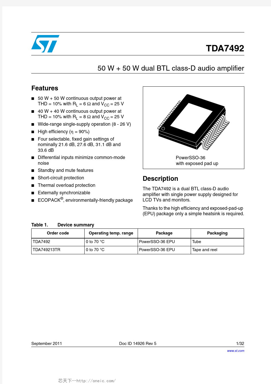
TDA7492
50 W + 50 W dual BTL class-D audio amplifier
Features
■50 W + 50 W continuous output power at THD = 10% with R L = 6 Ω and V CC = 25 V ■40 W + 40 W continuous output power at THD = 10% with R L = 8 Ω and V CC = 25 V ■Wide-range single-supply operation (8 - 26 V)■High efficiency (η = 90%)
■
Four selectable, fixed gain settings of nominally 21.6dB, 27.6dB, 31.1 dB and 33.6dB
■Differential inputs minimize common-mode noise
■Standby and mute features ■Short-circuit protection ■Thermal overload protection ■Externally synchronizable
■
ECOPACK ?, environmentally-friendly package
Description
The TDA7492 is a dual BTL class-D audio amplifier with single power supply designed for LCD TVs and monitors.
Thanks to the high efficiency and exposed-pad-up (EPU) package only a simple heatsink is required.
Table 1.Device summary
Order code
Operating temp. range Package
Packaging
TDA74920 to 70 °C PowerSSO-36 EPU T ube
TDA749213TR
0 to 70 °C
PowerSSO-36 EPU
T ape and reel
https://www.doczj.com/doc/a813465614.html,
Contents TDA7492
Contents
1Device block diagram . . . . . . . . . . . . . . . . . . . . . . . . . . . . . . . . . . . . . . . . 6
2Pin description . . . . . . . . . . . . . . . . . . . . . . . . . . . . . . . . . . . . . . . . . . . . . 7
2.1Pinout . . . . . . . . . . . . . . . . . . . . . . . . . . . . . . . . . . . . . . . . . . . . . . . . . . . . . 7
2.2Pin list . . . . . . . . . . . . . . . . . . . . . . . . . . . . . . . . . . . . . . . . . . . . . . . . . . . . . 8
3Electrical specifications . . . . . . . . . . . . . . . . . . . . . . . . . . . . . . . . . . . . . . 9
3.1Absolute maximum ratings . . . . . . . . . . . . . . . . . . . . . . . . . . . . . . . . . . . . . 9
3.2Thermal data . . . . . . . . . . . . . . . . . . . . . . . . . . . . . . . . . . . . . . . . . . . . . . . 9
3.3Electrical specifications . . . . . . . . . . . . . . . . . . . . . . . . . . . . . . . . . . . . . . . 9
4Characterization curves . . . . . . . . . . . . . . . . . . . . . . . . . . . . . . . . . . . . . 11
4.1Characterizations for 6-Ω loads . . . . . . . . . . . . . . . . . . . . . . . . . . . . . . . . 11
4.2Characterizations for 8-Ω loads . . . . . . . . . . . . . . . . . . . . . . . . . . . . . . . . 15
4.3Characterizations for 4-Ω loads . . . . . . . . . . . . . . . . . . . . . . . . . . . . . . . . 18
4.4Test board . . . . . . . . . . . . . . . . . . . . . . . . . . . . . . . . . . . . . . . . . . . . . . . . . 21 5Applications circuit . . . . . . . . . . . . . . . . . . . . . . . . . . . . . . . . . . . . . . . . . 22
6Applications information . . . . . . . . . . . . . . . . . . . . . . . . . . . . . . . . . . . . 23
6.1Mode selection . . . . . . . . . . . . . . . . . . . . . . . . . . . . . . . . . . . . . . . . . . . . . 23
6.2Gain setting . . . . . . . . . . . . . . . . . . . . . . . . . . . . . . . . . . . . . . . . . . . . . . . 24
6.3Input resistance and capacitance . . . . . . . . . . . . . . . . . . . . . . . . . . . . . . . 24
6.4Internal and external clocks . . . . . . . . . . . . . . . . . . . . . . . . . . . . . . . . . . . 25
6.4.1Master mode (internal clock) . . . . . . . . . . . . . . . . . . . . . . . . . . . . . . . . . 25
6.4.2Slave mode (external clock) . . . . . . . . . . . . . . . . . . . . . . . . . . . . . . . . . . 25
6.5Output low-pass filter . . . . . . . . . . . . . . . . . . . . . . . . . . . . . . . . . . . . . . . . 26
6.6Protection functions . . . . . . . . . . . . . . . . . . . . . . . . . . . . . . . . . . . . . . . . . 27
6.7Diagnostic output . . . . . . . . . . . . . . . . . . . . . . . . . . . . . . . . . . . . . . . . . . . 27
6.8Heatsink requirements . . . . . . . . . . . . . . . . . . . . . . . . . . . . . . . . . . . . . . . 28 7Package mechanical data . . . . . . . . . . . . . . . . . . . . . . . . . . . . . . . . . . . 29
2/32 Doc ID 14926 Rev 5
TDA7492Contents 8Revision history . . . . . . . . . . . . . . . . . . . . . . . . . . . . . . . . . . . . . . . . . . . 31
Doc ID 14926 Rev 53/32
List of tables TDA7492 List of tables
Table 1.Device summary. . . . . . . . . . . . . . . . . . . . . . . . . . . . . . . . . . . . . . . . . . . . . . . . . . . . . . . . . . 1 Table 2.Pin description list. . . . . . . . . . . . . . . . . . . . . . . . . . . . . . . . . . . . . . . . . . . . . . . . . . . . . . . . . 8 Table 3.Absolute maximum ratings. . . . . . . . . . . . . . . . . . . . . . . . . . . . . . . . . . . . . . . . . . . . . . . . . . 9 Table 4.Thermal data. . . . . . . . . . . . . . . . . . . . . . . . . . . . . . . . . . . . . . . . . . . . . . . . . . . . . . . . . . . . . 9 Table 5.Electrical specifications. . . . . . . . . . . . . . . . . . . . . . . . . . . . . . . . . . . . . . . . . . . . . . . . . . . . . 9 Table 6.Mode settings. . . . . . . . . . . . . . . . . . . . . . . . . . . . . . . . . . . . . . . . . . . . . . . . . . . . . . . . . . . 23 Table 7.Gain settings. . . . . . . . . . . . . . . . . . . . . . . . . . . . . . . . . . . . . . . . . . . . . . . . . . . . . . . . . . . . 24 Table 8.How to set up SYNCLK . . . . . . . . . . . . . . . . . . . . . . . . . . . . . . . . . . . . . . . . . . . . . . . . . . . 25 Table 9.PowerSSO-36 EPU dimensions. . . . . . . . . . . . . . . . . . . . . . . . . . . . . . . . . . . . . . . . . . . . . 30 Table 10.Document revision history . . . . . . . . . . . . . . . . . . . . . . . . . . . . . . . . . . . . . . . . . . . . . . . . . 31 4/32 Doc ID 14926 Rev 5
TDA7492List of figures List of figures
Figure 1.Internal block diagram (showing one channel only) . . . . . . . . . . . . . . . . . . . . . . . . . . . . . . . 6 Figure 2.Pin connections (top view, PCB view) . . . . . . . . . . . . . . . . . . . . . . . . . . . . . . . . . . . . . . . . . 7 Figure 3.Output power vs. supply voltage . . . . . . . . . . . . . . . . . . . . . . . . . . . . . . . . . . . . . . . . . . . . 11 Figure 4.THD vs. output power (1kHz) . . . . . . . . . . . . . . . . . . . . . . . . . . . . . . . . . . . . . . . . . . . . . . 12 Figure 5.THD vs. output power (100Hz) . . . . . . . . . . . . . . . . . . . . . . . . . . . . . . . . . . . . . . . . . . . . . 12 Figure 6.THD vs. frequency . . . . . . . . . . . . . . . . . . . . . . . . . . . . . . . . . . . . . . . . . . . . . . . . . . . . . . . 13 Figure 7.Frequency response . . . . . . . . . . . . . . . . . . . . . . . . . . . . . . . . . . . . . . . . . . . . . . . . . . . . . 13 Figure 8.Crosstalk . . . . . . . . . . . . . . . . . . . . . . . . . . . . . . . . . . . . . . . . . . . . . . . . . . . . . . . . . . . . . . 13 Figure 9.FFT performance (0 dB) . . . . . . . . . . . . . . . . . . . . . . . . . . . . . . . . . . . . . . . . . . . . . . . . . . 14 Figure 10.FFT performance (-60 dB) . . . . . . . . . . . . . . . . . . . . . . . . . . . . . . . . . . . . . . . . . . . . . . . . . 14 Figure 11.Output power vs. supply voltage . . . . . . . . . . . . . . . . . . . . . . . . . . . . . . . . . . . . . . . . . . . . 15 Figure 12.THD vs. output power (1 kHz) . . . . . . . . . . . . . . . . . . . . . . . . . . . . . . . . . . . . . . . . . . . . . . 15 Figure 13.THD vs. output (100Hz) . . . . . . . . . . . . . . . . . . . . . . . . . . . . . . . . . . . . . . . . . . . . . . . . . . 16 Figure 14.THD vs. frequency . . . . . . . . . . . . . . . . . . . . . . . . . . . . . . . . . . . . . . . . . . . . . . . . . . . . . . . 16 Figure 15.Frequency response . . . . . . . . . . . . . . . . . . . . . . . . . . . . . . . . . . . . . . . . . . . . . . . . . . . . . 16 Figure 16.Crosstalk . . . . . . . . . . . . . . . . . . . . . . . . . . . . . . . . . . . . . . . . . . . . . . . . . . . . . . . . . . . . . . 17 Figure 17.FFT performance (0 dB). . . . . . . . . . . . . . . . . . . . . . . . . . . . . . . . . . . . . . . . . . . . . . . . . . . 17 Figure 18.FFT performance (-60 dB) . . . . . . . . . . . . . . . . . . . . . . . . . . . . . . . . . . . . . . . . . . . . . . . . . 17 Figure 19.Output power vs. supply voltage . . . . . . . . . . . . . . . . . . . . . . . . . . . . . . . . . . . . . . . . . . . . 18 Figure 20.THD vs. output power (1 kHz) . . . . . . . . . . . . . . . . . . . . . . . . . . . . . . . . . . . . . . . . . . . . . . 18 Figure 21.THD vs. output (100Hz) . . . . . . . . . . . . . . . . . . . . . . . . . . . . . . . . . . . . . . . . . . . . . . . . . . 19 Figure 22.THD vs. frequency . . . . . . . . . . . . . . . . . . . . . . . . . . . . . . . . . . . . . . . . . . . . . . . . . . . . . . . 19 Figure 23.Frequency response . . . . . . . . . . . . . . . . . . . . . . . . . . . . . . . . . . . . . . . . . . . . . . . . . . . . . 19 Figure 24.Crosstalk . . . . . . . . . . . . . . . . . . . . . . . . . . . . . . . . . . . . . . . . . . . . . . . . . . . . . . . . . . . . . . 20 Figure 25.FFT performance (0 dB). . . . . . . . . . . . . . . . . . . . . . . . . . . . . . . . . . . . . . . . . . . . . . . . . . . 20 Figure 26.FFT performance (-60 dB) . . . . . . . . . . . . . . . . . . . . . . . . . . . . . . . . . . . . . . . . . . . . . . . . . 20 Figure 27.Test board layout . . . . . . . . . . . . . . . . . . . . . . . . . . . . . . . . . . . . . . . . . . . . . . . . . . . . . . . . 21 Figure 28.Applications circuit for class-D amplifier . . . . . . . . . . . . . . . . . . . . . . . . . . . . . . . . . . . . . . 22 Figure 29.Standby and mute circuits . . . . . . . . . . . . . . . . . . . . . . . . . . . . . . . . . . . . . . . . . . . . . . . . . 23 Figure 30.Turn on/off sequence for minimizing speaker “pop” . . . . . . . . . . . . . . . . . . . . . . . . . . . . . 23 Figure 31.Device input circuit and frequency response . . . . . . . . . . . . . . . . . . . . . . . . . . . . . . . . . . . 24 Figure 32.Master and slave connection . . . . . . . . . . . . . . . . . . . . . . . . . . . . . . . . . . . . . . . . . . . . . . . 25 Figure 33.Typical LC filter for a 8-Ω speaker . . . . . . . . . . . . . . . . . . . . . . . . . . . . . . . . . . . . . . . . . . . 26 Figure 34.Typical LC filter for a 4-Ω speaker . . . . . . . . . . . . . . . . . . . . . . . . . . . . . . . . . . . . . . . . . . . 26 Figure 35.Behavior of pin DIAG for various protection conditions . . . . . . . . . . . . . . . . . . . . . . . . . . . 27 Figure 36.PowerSSO-36 EPU outline drawing . . . . . . . . . . . . . . . . . . . . . . . . . . . . . . . . . . . . . . . . . 29
Doc ID 14926 Rev 55/32
Device block diagram TDA7492 1 Device block diagram
Figure1 shows the block diagram of one of the two identical channels of the TDA7492.
Figure 1.Internal block diagram (showing one channel only)
6/32 Doc ID 14926 Rev 5
TDA7492Pin description
Doc ID 14926 Rev 57/32
2 Pin description
2.1 Pinout
Figure 2.
Pin connections (top view, PCB view)
123456789
101112131415161718
2829303132333435
36192021222324252627VSS SUB GND OUTPB OUTPB PGNDB PGNDB PVCCB PVCCB OUTNB OUTNB
OUTNA OUTNA PVCCA PVCCA PGNDA PGNDA OUTPA OUTPA PGND VDDPW
STBY MUTE INPA INNA ROSC SYNCLK VDDS SGND DIAG SVR GAIN0GAIN1INPB INNB VREF SVCC
EP
exposed pad up Connect to ground
Pin description TDA7492
8/32 Doc ID 14926 Rev 5
2.2 Pin list
Table 2.
Pin description list
Number Name Type Description
1SUB_GND PWR Connect to the frame
2,3OUTPB O Positive PWM for right channel 4,5PGNDB PWR Power stage ground for right channel 6,7PVCCB PWR Power supply for right channel 8,9OUTNB O Negative PWM output for right channel 10,11OUTNA O Negative PWM output for left channel 12,13PVCCA PWR Power supply for left channel 14,15PGNDA PWR Power stage ground for left channel 16,17OUTP A O Positive PWM output for left channel 18PGND PWR Power stage ground
19VDDPW O 3.3-V (nominal) regulator output referred to ground for power stage
20STBY I Standby mode control 21MUTE I Mute mode control
22INP A I Positive differential input of left channel 23INNA I Negative differential input of left channel 24ROSC O Master oscillator frequency-setting pin 25SYNCLK I/O Clock in/out for external oscillator
26VDDS O 3.3-V (nominal) regulator output referred to ground for signal blocks 27SGND PWR Signal ground
28DIAG O Open-drain diagnostic output 29SVR O Supply voltage rejection 30GAIN0I Gain setting input 131GAIN1I Gain setting input 2
32INPB I Positive differential input of right channel 33INNB I Negative differential input of right channel 34VREF O Half VDDS (nominal) referred to ground 35SVCC PWR Signal power supply
36VSS O 3.3-V (nominal) regulator output referred to power supply -EP
-Exposed pad for heatsink, to be connected to GND
TDA7492Electrical specifications
Doc ID 14926 Rev 59/32
3 Electrical specifications
3.1
Absolute maximum ratings
3.2 Thermal data
3.3 Electrical specifications
Unless otherwise stated, the results in Table 5 below are given for the conditions:
V CC =25V , R L (load) = 8 Ω, R OSC = R3 = 39 k Ω, C8 = 100 nF , f = 1 kHz, G V = 21.6 dB and Tamb =25 °C.
Table 3.
Absolute maximum ratings
Symbol Parameter
Value
Unit V CC DC supply voltage for pins PVCCA, PVCCB, SVCC 30V V I Voltage limits for input pins STBY , MUTE, INNA, INP A,
INNB, INPB, GAIN0, GAIN1-0.3 - 3.6V T op Operating temperature 0 to 70°C T j Junction temperature -40 to 150°C T stg
Storage temperature
-40 to 150
°C
Table 4.
Thermal data
Symbol Parameter
Min
Typ Max Unit R th j-case
Thermal resistance, junction to case
-2
3
°C/W
Table 5.
Electrical specifications
Symbol Parameter
Condition
Min Typ
Max Unit V CC Supply voltage for
pins PVCCA, PVCCB, SVCC -8-26V I q Total quiescent current Without LC -2635mA I qSTBY Quiescent current in standby -- 2.5 5.0μA V OS Output offset voltage
Play mode --±100mV Mute mode
--±60I OCP Overcurrent protection threshold R L = 0 Ω 4.8 6.0-A T j
Junction temperature at thermal
shutdown --150-°C R i Input resistance
Differential input
4860-k ΩV OVP
Overvoltage protection threshold -
28
29-V
Electrical specifications
TDA7492
10/32 Doc ID 14926 Rev 5
V UVP Undervoltage protection threshold
---7V R dsON
Power transistor on resistance
High side -0.2-Ω
Low side -0.2-P o
Output power THD = 10%-40-W
THD = 1%
-32-P o
Output power
R L = 6 Ω, THD = 10%, V CC =25V
-50-W
R L = 6 Ω, THD = 1% V CC =25V -40-P D Dissipated power P o =40W +40 W,THD =10%-8.0-W ηEfficiency
P o = 40 W + 40W 8090-%THD
Total harmonic distortion
P o = 1 W
-0.10.4%G V
Closed-loop gain
GAIN0 = L, GAIN1 = L
20.621.622.6dB GAIN0 = L, GAIN1 = H 26.627.628.6GAIN0 = H, GAIN1 = L 30.131.132.1GAIN0 = H, GAIN1 = H
32.633.634.6ΔG V Gain matching ---±1dB CT Cross talk f = 1 kHz
-50-dB eN Total input noise
A Curve, G V = 20 d
B -20-μV f = 22 Hz to 22 kHz -2535SVRR Supply voltage rejection ratio fr = 100 Hz, Vr = 0.5 V ,
C SVR = 10 μF 4050-dB T r , T f Rise and fall times --50-ns f SW Switching frequency Internal oscillator
290310330kHz f SWR Output switching frequency Range
With internal oscillator (1)250-400kHz With external oscillator (2)250-400V inH Digital input high (H)- 2.3--V V inL Digital input low (L)--0.8A MUTE
Mute attenuation
V MUTE = 1 V
60
80-dB
1.f SW = 106 / ((16 * R OSC + 182) * 4) kHz, f SYNCLK = 2 * f SW with R3 = 39k Ω (see Figure 28.).
2.f SW = f SYNCLK / 2 with the frequency of the external oscillator.
Table 5.
Electrical specifications (continued)
Symbol Parameter
Condition
Min
Typ
Max Unit
TDA7492Characterization curves
Doc ID 14926 Rev 511/32
4 Characterization curves
The general test conditions used for producing the characterization curves can be
summarized as follows:
Test board: SZ LAB TDA7492 slug-up demo board
Test frequency: 1 kHz (also 100 Hz for THD vs. output power only)Output power: 1 W
●
For 6-Ω loads –test voltage: 25 V
–
LC filter: L = 22 μH and C = 220 nF ●
For 8-Ω loads –test voltage: 25 V
–
LC filter: L = 33 μH and C = 220 nF ●
For 4-Ω loads –test voltage: 20 V
–
LC filter: L = 15 μH and C = 470 nF .
Figure 28 on page 22 shows the circuit with which the characterization curves, shown in the next sections, were measured. Figure 27 on page 21 shows the PCB layout.
4.1 Characterizations for 6-Ω loads
Te s t condition s :Vcc = 15 -25 V, RL = 6 Ω,
Ro s c = 39 k Ω, Co s c = 100 nF,f = 1 kHz,Gv = 30 dB,T a m b = 25r C
S pecific a tion limit: Typic a l:
V s = 25 V, RL = 6 Ω,Po = 50 W a tTHD = 10%,Po = 40 W a tTHD = 1%
3RXW YV 9FF
9FF 9
3R X W :
10% THD
1% THD
Characterization curves TDA7492
12/32 Doc ID 14926 Rev 5
TDA7492Characterization curves
Doc ID 14926 Rev 513/32
Characterization curves TDA7492
14/32 Doc ID 14926 Rev 5
TDA7492Characterization curves 4.2 Characterizations for 8-Ω loads
Doc ID 14926 Rev 515/32
Characterization curves TDA7492
16/32 Doc ID 14926 Rev 5
TDA7492Characterization curves
Doc ID 14926 Rev 517/32
Characterization curves TDA7492 4.3 Characterizations for 4-Ω loads
18/32 Doc ID 14926 Rev 5
TDA7492Characterization curves
Doc ID 14926 Rev 519/32
Characterization curves TDA7492
20/32 Doc ID 14926 Rev 5