Integrated Silicon Solution, Inc. — https://www.doczj.com/doc/a813359263.html, — 1-800-379-4774
1
Rev.00B 06/21/06
ISSI
?
Copyright ? 2006 Integrated Silicon Solution, Inc. All rights reserved. ISSI reserves the right to make changes to this specification and its products at any time without notice. ISSI assumes no liability arising out of the application or use of any information, products or services described herein. Customers are advised to obtain the latest version of this device specification before relying on any published information and before placing orders for products.
IS62WV20488ALL IS62WV20488BLL
2M x 8 HIGH-SPEED LOW POWER CMOS STATIC RAM
PREL IMINARY INFORMATION
JUL Y 2006
FEATURES
?High-speed access times: 25, 35 ns
?High-performance, low-power CMOS process ?Multiple center power and ground pins for greater noise immunity
?Fully static operation: no clock or refresh required
?TTL compatible inputs and outputs ?Single power supply
– V DD 1.65V to 2.2V (IS62WV20488ALL) speed = 35ns for Vcc = 1.65V to 2.2V – V DD 2.4V to 3.6V (IS62WV20488BLL) speed = 25ns for Vcc = 2.4V to 3.6V ?Packages available:
– 48-ball miniBGA (9mm x 11mm )– 44-pin TSOP (Type II)
?Industrial Temperature Support ?Lead-free available
DESCRIPTION
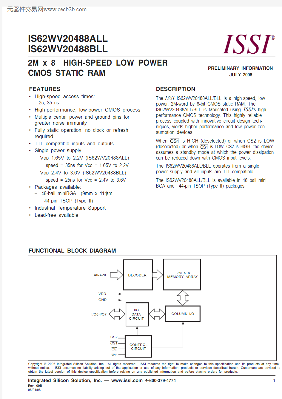
The ISSI IS62WV20488ALL/BLL is a high-speed, low
power, 2M-word by 8-bit CMOS static RAM. The
IS62WV20488ALL/BLL is fabricated using ISSI 's high-performance CMOS technology. This highly reliable process coupled with innovative circuit design tech-niques, yields higher performance and low power con-sumption devices.
When CS1 is HIGH (deselected) or when CS2 is LOW (deselected) or when CS1 is LOW, CS2 is HI GH, the device assumes a standby mode at which the power dissipation can be reduced down with CMOS input levels.The IS62WV20488ALL/BLL operates from a single power supply and all inputs are TTL-compatible.The IS62WV20488ALL/BLL is available in 48 ball mini BGA and 44-pin TSOP (Type II) packages.
2Integrated Silicon Solution, Inc. — https://www.doczj.com/doc/a813359263.html, — 1-800-379-4774
Rev.00B 06/21/06
ISSI
?
IS62WV20488ALL IS62WV20488BLL
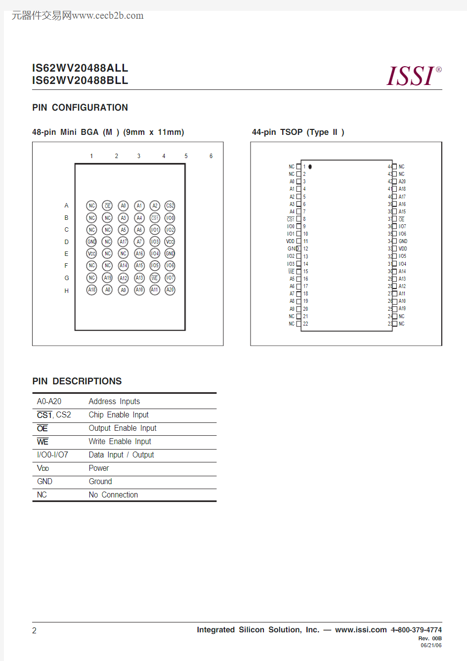
PIN DESCRIPTIONS
A0-A20Address Inputs CS1, CS2Chip Enable Input OE Output Enable Input WE Write Enable Input I/O0-I/O7Data Input / Output V DD Power GND Ground NC
No Connection
48-pin Mini BGA (M ) (9mm x 11mm)
44-pin TSOP (Type II )
PIN CONFIGURATION
Integrated Silicon Solution, Inc. — https://www.doczj.com/doc/a813359263.html, — 1-800-379-4774
3
Rev.00B 06/21/06
ISSI
?
IS62WV20488ALL IS62WV20488BLL
ABSOLUTE MAXIMUM RATINGS (1)
Symbol Parameter
Value
Unit V TERM Terminal Voltage with Respect to GND –0.5 to V DD + 0.5V V DD V DD Relates to GND –0.3 to 4.0V T STG Storage Temperature –65 to +150
°C P T
Power Dissipation
1.0
W
Notes:
1.Stress greater than those listed under ABSOLUTE MAXIMUM RATINGS may cause permanent damage to the device. This is a stress rating only and functional operation of the device at these or any other conditions above those indicated in the operational sections of this specification is not implied. Exposure to absolute maximum rating conditions for extended periods may affect reliability.
TRUTH TABL E
Mode
WE CS1CS2OE I/O Operation
V DD Current Not Selected X H X X High-Z I SB 1, I SB 2
(Power-down)X X L X Output Disabled H L H H High-Z I CC Read H L H L D OUT I CC Write
L
L
H
X
D IN
I CC
CAPACITANCE (1,2)
Symbol Parameter Conditions Max.Unit C IN I nput Capacitance V IN = 0V 6pF C I/O
I nput/Output Capacitance
V OUT = 0V
8
pF
Notes:
1.Tested initially and after any design or process changes that may affect these parameters.
2.Test conditions: T A = 25°C, f = 1 MHz, V DD =
3.3V.
4Integrated Silicon Solution, Inc. — https://www.doczj.com/doc/a813359263.html, — 1-800-379-4774
Rev.00B 06/21/06
ISSI
?
IS62WV20488ALL IS62WV20488BLL
OPERATING RANGE (V DD ) (IS62WV20488BLL)(1)
Range Ambient Temperature V DD (25 n S )
Commercial 0°C to +70°C 2.4V-3.6V Industrial –40°C to +85°C
2.4V-
3.6V
Note:
1. When operated in the range of
2.4V-
3.6V, the device meets 25ns. When operated in the range of 3.3V + 5%, the device meets 15ns.
OPERATING RANGE (V DD ) (IS62WV20488ALL)
Range Ambient Temperature V DD (35 n S )
Commercial 0°C to +70°C 1.65V-2.2V Industrial –40°C to +85°C
1.65V-
2.2V
Integrated Silicon Solution, Inc. — https://www.doczj.com/doc/a813359263.html, — 1-800-379-4774
5
Rev.00B 06/21/06
ISSI
?
IS62WV20488ALL IS62WV20488BLL
DC ELECTRICAL CHARACTERISTICS (Over Operating Range)V DD = 2.4V-3.6V
Symbol Parameter
Test Conditions
Min.Max.Unit
V OH Output HIGH Voltage V DD = Min., I OH = –1.0 mA 1.8—V V OL Output LOW Voltage V DD = Min., I OL = 1.0 mA
—0.4V V IH Input HIGH Voltage 2.0V DD + 0.3V V IL Input LOW Voltage (1)–0.30.8V I LI I nput Leakage GND ≤ V IN ≤ V DD
–11μA I LO
Output Leakage
GND ≤ V OUT ≤ V DD , Outputs Disabled –1
1
μA
Note:
1. V IL (min.) = –0.3V DC; V IL (min.) = –
2.0V AC (pulse width - 2.0 ns). Not 100% tested.
V IH (max.) = V DD + 0.3V DC; V IH (max.) = V DD + 2.0V AC (pulse width - 2.0 ns). Not 100% tested.
DC ELECTRICAL CHARACTERISTICS (Over Operating Range)V DD = 1.65V-2.2V
Symbol Parameter
Test Conditions V DD Min.Max.Unit V OH Output HIGH Voltage I OH = -0.1 mA 1.65-2.2V 1.4—V V OL Output LOW Voltage I OL = 0.1 mA
1.65-
2.2V —0.2V V IH Input HIGH Voltage 1.65-2.2V 1.4V DD + 0.2V V IL (1)Input LOW Voltage 1.65-2.2V
–0.20.4V I LI I nput Leakage GND ≤ V IN ≤ V DD
–11μA I LO
Output Leakage
GND ≤ V OUT ≤ V DD , Outputs Disabled –1
1
μA
Note:
1. V IL (min.) = –0.3V DC; V IL (min.) = –
2.0V AC (pulse width - 2.0 ns). Not 100% tested.
V IH (max.) = V DD + 0.3V DC; V IH (max.) = V DD + 2.0V AC (pulse width - 2.0 ns). Not 100% tested.
6Integrated Silicon Solution, Inc. — https://www.doczj.com/doc/a813359263.html, — 1-800-379-4774
Rev.00B 06/21/06
ISSI
?
IS62WV20488ALL IS62WV20488BLL
POWER SUPPLY CHARACTERISTICS (1) (Over Operating Range)
-25-35Symbol Parameter Test Conditions Min.Max.
Min.Max.Unit I CC
V DD Dynamic Operating V DD = Max.,
Com.—30—25mA
Supply Current I OUT = 0 mA, f = f MAX Ind.—35—30typ.(2)
15I CC 1Operating V DD = Max.,Com.—10—10mA Supply Current I OUT = 0 mA, f = 0
Ind.
—15—15I SB 1
TTL Standby Current V DD = Max.,Com.—10—10mA
(TTL I nputs)V IN = V IH or V IL Ind.—
12
—12CS1 ≥ V IH , f = 0, CS2 = V IL I SB 2
CMOS Standby
V DD = Max.,
Com.— 1.5— 1.5mA
Current (CMOS I nputs)
CS1 ≥ V DD – 0.2V,Ind.— 1.5—
1.5
CS2 ≤ 0.2V,
typ.(2)
0.8
V IN ≥ V DD – 0.2V, or V IN ≤ 0.2V , f = 0
Note:
1. At f = f MAX , address and data inputs are cycling at the maximum frequency, f = 0 means no input lines change.
2. Typical values are measured at V DD =
3.0V, T A = 25o C and not 100% tested.
Integrated Silicon Solution, Inc. — https://www.doczj.com/doc/a813359263.html, — 1-800-379-4774
7
Rev.00B 06/21/06
ISSI
?
IS62WV20488ALL IS62WV20488BLL
AC TEST LOADS
Figure 1
AC TEST CONDITIONS (LOW POWER)
Parameter
Unit Unit (2.4V-3.6V)(1.65V-2.2V)Input Pulse Level
0.4V to V DD -0.3V
0.4V to V DD -0.2V
Input Rise and Fall Times 1.5ns 1.5ns Input and Output Timing V DD /2V DD /2and Reference Level (V Ref )Output Load
See Figures 1 and 2
See Figures 1 and 2
8Integrated Silicon Solution, Inc. — https://www.doczj.com/doc/a813359263.html, — 1-800-379-4774
Rev.00B 06/21/06
ISSI
?
IS62WV20488ALL IS62WV20488BLL
READ CYCLE SWITCHING CHARACTERISTICS (1) (Over Operating Range)
25ns 35ns
Symbol
Parameter Min.Max.Min.Max.Unit t RC Read Cycle Time 25—35—ns t AA Address Access Time —25—35ns t OHA Output Hold Time 4—4—ns t ACS1/t ACS2CS1/CS2 Access Time —25—35ns t DOE OE Access Time —12—15ns t HZOE (2)OE to High-Z Output —8—10ns t LZOE (2)
OE to Low-Z Output 5—5—ns t HZCS1/t HZCS2(2)CS1/CS2 to High-Z Output 08010ns t LZCS1/t LZCS2(2)
CS1/CS2 to Low-Z Output
10
—
10
—
ns
Notes:
1.Test c onditions a ssume s ignal t ransition t imes o f 5 n s o r l ess, t iming r eference l evels o f 0.9V/1.5V, i nput p ulse l evels o f 0.4 t o V DD -0.2V/0.4V t o V DD -0.3V a nd output l oading s pecified i n F igure 1.
2.Tested w ith t he l oad i n F igure 2. T ransition i s m easured ±500 m V f rom s teady-state v oltage. N ot 100% t ested.
AC WAVEFORMS
READ CYCLE NO. 1(1,2) (Address Controlled) (CS1 = OE = V IL , CS2 = WE = V IH )
Integrated Silicon Solution, Inc. — https://www.doczj.com/doc/a813359263.html, — 1-800-379-4774
9
Rev.00B 06/21/06
ISSI
?
IS62WV20488ALL IS62WV20488BLL
AC WAVEFORMS
READ CYCLE NO. 2(1,3)(CS1, CS2, OE Controlled)
Notes:
1.WE is HI GH for a Read Cycle.
2.The device is continuously selected. OE , CS1= V IL . C S2=WE =V IH .
3.Address i s v alid p rior t o o r c oincident w ith C S1 L OW a nd CS2 H I GH t ransition.
10Integrated Silicon Solution, Inc. — https://www.doczj.com/doc/a813359263.html, — 1-800-379-4774
Rev.00B 06/21/06
ISSI
?
IS62WV20488ALL IS62WV20488BLL
WRITE CYCLE SWITCHING CHARACTERISTICS (1,2) (Over Operating Range)
25 ns 35 ns Symbol
Parameter Min.Max.Min.Max.Unit t WC
Write Cycle Time
25—35—ns t SCS1/t SCS2CS1/CS2 to Write End
18—25—ns t AW Address Setup Time to Write End 15—25—ns t HA Address Hold from Write End 0—0—ns t SA Address Setup Time 0—0—ns t PWE (4)WE Pulse Width 18—30—ns t SD Data Setup to Write End 12—15—ns t HD
Data Hold from Write End 0—0—ns t HZWE (3)WE LOW to High-Z Output —12—20ns t LZWE (3)
WE HIGH to Low-Z Output
5
—
5
—
ns
Notes:
1.Test c onditions a ssume s ignal t ransition t imes o f 5 n s o r l ess, t iming r eference l evels o f 0.9V/1.5V, i nput p ulse l evels o f 0.4 t o V DD -0.2V/0.4V t o V DD -0.3V a nd output l oading s pecified i n F igure 1.
2.The internal write time is defined by the overlap of CS1 LOW, CS2 HIGH and UB or LB , and WE LOW. All signals must be in valid states to initiate a Write, but any one can go inactive to terminate the Write. The Data Input Setup and Hold timing are referenced to the rising or falling edge of the signal that terminates the write.
3.Tested w ith t he l oad i n F igure 2. T ransition i s m easured ±500 m V f rom s teady-state v oltage. N ot 100% t ested.
4. t PWE > t HZWE + t SD when OE is LOW.
AC WAVEFORMS
WRITE CYCLE NO. 1 (CS1/CS2 Controlled, OE = HIGH or LOW )
Integrated Silicon Solution, Inc. — https://www.doczj.com/doc/a813359263.html, — 1-800-379-4774
11
Rev.00B 06/21/06
ISSI
?
IS62WV20488ALL IS62WV20488BLL
AC WAVEFORMS
WRITE CYCLE NO. 2 (WE Controlled: OE is HIGH During Write Cycle)
12Integrated Silicon Solution, Inc. — https://www.doczj.com/doc/a813359263.html, — 1-800-379-4774
Rev.00B 06/21/06
ISSI
?
IS62WV20488ALL IS62WV20488BLL
DATA RETENTION SWITCHING CHARACTERISTICS
Symbol Parameter
Test Condition
Min.Typ.(1)Max.
Unit V DR Vcc for Data Retention See Data Retention Waveform 1.2 3.6V I DR Data Retention Current Vcc = 1.2V, CS1/CS2 ≥ Vcc – 0.2V —0.5
1.5mA t SDR Data Retention Setup Time See Data Retention Waveform 0—ns t RDR
Recovery Time
See Data Retention Waveform
t RC
—
ns
Note:
1. Typical values are measured at V DD = 3.0V, T A = 25o C and not 100% tested.
DATA RETENTION WAVEFORM (CS1 Controlled)
DATA RETENTION WAVEFORM (CS2 Controlled)
Integrated Silicon Solution, Inc. — https://www.doczj.com/doc/a813359263.html, — 1-800-379-4774
13
Rev.00B 06/21/06
ISSI
?
IS62WV20488ALL IS62WV20488BLL
ORDERING INFORMATION Industrial Range: -40°C to +85°C Voltage Range: 2.4V to 3.6V
Speed (ns)
Order Part No.
Package
25
IS62WV20488BLL-25MI 48 mini BGA (9mm x 11mm)
IS62WV20488BLL-25MLI 48 mini BGA (9mm x 11mm), Lead-free IS62WV20488BLL-25TI TSOP (Type II)
IS62WV20488BLL-25TLI
TSOP (Type II), Lead-free
Industrial Range: -40°C to +85°C Voltage Range: 1.65V to 2.2V
Speed (ns)
Order Part No.Package
35
IS62WV20488ALL-35MI 48 mini BGA (9mm x 11mm)IS62WV20488ALL-35TI
TSOP (Type II)
PACKAGING INFORMATION
ISSI
?
Integrated Silicon Solution, Inc. — https://www.doczj.com/doc/a813359263.html, — 1-800-379-4774
Rev.D 01/15/03
without notice. ISSI assumes no liability arising out of the application or use of any information, products or services described herein. Customers are advised to obtain the latest version of this device specification before relying on any published information and before placing orders for products.
Mini Ball Grid Array
Package Code: M (48-pin)
PACKAGING INFORMATION
ISSI
?
2Integrated Silicon Solution, Inc. — https://www.doczj.com/doc/a813359263.html, — 1-800-379-4774
Rev. D 01/15/03
mBGA - 7.2mm x 8.7mm
MILLIMETERS
INCHES Sym.
Min.Typ.Max.
Min.Typ.Max.
N0.Leads 48A —— 1.20— —0.047A10 .24—0.300.009 —0.012A20.60——
0.024
—
—
D 8.60
8.708.800.3390.3430.346
D1 5.25BSC 0.207BSC E 7.107.207.300.2800.2830.287
E1 3.75BSC 0.148BSC e 0.75BSC 0.030BSC b
0.30
0.35
0.400.0120.0140.016
mBGA - 9mm x 11mm
MILLIMETERS INCHES Sym.
Min.Typ.Max.
Min.Typ.Max.
N0.Leads
48
A —— 1.20 —
—0.047A1 0.24—0.300.009 —0.012A20.60
——
0.024
—
—
D 10.9011.0011.100.4290.4330.437
D1 5.25BSC 0.207BSC E 8.90
9.00
9.10
0.3500.3540.358
E1 3.75BSC 0.148BSC e 0.75BSC 0.030BSC b
0.30
0.35
0.400.0120.0140.016
mBGA - 6mm x 8mm
MILLIMETERS
INCHES Sym.
Min.Typ.Max.
Min.Typ.Max.
N0.Leads 48A —— 1.20.— —0.047A1 0.25—0.400.010 —0.016A20.60——
0.024
—
—
D 7.90
8.008.10
0.3110.3140.319
D1 5.60BSC 0.220BSC E 5.90 6.00 6.100.2320.2360.240
E1 4.00BSC 0.157BSC e 0.80BSC 0.031BSC b
0.40
0.45
0.500.0160.0180.020
Mini Ball Grid Array
Package Code: M (48-pin)
PACKAGING INFORMATION
ISSI
?
Integrated Silicon Solution, Inc. — https://www.doczj.com/doc/a813359263.html, — 1-800-379-4774
Rev.F 06/18/03
Copyright ? 2003 Integrated Silicon Solution, Inc. All rights reserved. ISSI reserves the right to make changes to this specification and its products at any time
without notice. ISSI assumes no liability arising out of the application or use of any information, products or services described herein. Customers are advised to obtain the latest version of this device specification before relying on any published information and before placing orders for products.
Plastic TSOP
Package Code: T (Type II)