
MGCM01
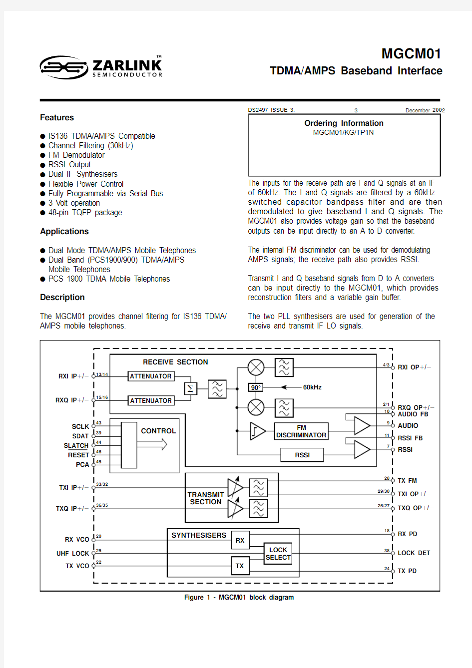
TDMA/AMPS Baseband Interface DS2497 ISSUE 3.3 December 2002Ordering Information MGCM01/KG/TP1N The inputs for the receive path are I and Q signals at an IF of 60kHz. The I and Q signals are filtered by a 60kHz switched capacitor bandpass filter and are then demodulated to give baseband I and Q signals. The MGCM01 also provides voltage gain so that the baseband outputs can be input directly to an A to D converter.The internal FM discriminator can be used for demodulating
AMPS signals; the receive path also provides RSSI.Transmit I and Q baseband signals from D to A converters
can be input directly to the MGCM01, which provides
reconstruction filters and a variable gain buffer.
The two PLL synthesisers are used for generation of the
receive and transmit IF LO signals.Features
q
IS136 TDMA/AMPS Compatible q
Channel Filtering (30kHz)q
FM Demodulator q
RSSI Output q
Dual IF Synthesisers q
Flexible Power Control q
Fully Programmable via Serial Bus q
3 Volt operation q 48-pin TQFP package
Applications
q Dual Mode TDMA/AMPS Mobile Telephones
q Dual Band (PCS1900/900) TDMA/AMPS Mobile Telephones q PCS 1900 TDMA Mobile Telephones Description The MGCM01 provides channel filtering for IS136 TDMA/AMPS mobile telephones.
Figure 1 - MGCM01 block diagram
MGCM01
Figure 2 - Pin connections - top view
Name RXQ OP-RXQ OP+ RXI OP-RXI OP+ GND
V DD RSSI GND AUDIO AUDIO FB RSSI FB GND
RXI IP+ RXI IP-RXQ IP+ RXQ IP-V DD
RX PD GND
RX VCO GND
TX VCO V DD
TX PD Type
O
O
O
O
GND
PWR
O
GND
O
I
I
GND
I
I
I
I
PWR
O
GND
I
GND
I
PWR
O
Description
Baseband receive Q output-
Baseband receive Q output+
Baseband receive I output-
Baseband receive I output+
Ground (substrate connection)
Power - RSSI/demodulator
RSSI output
Ground - RSSI/demodulator
Demodulator audio/data output
Demodulator feedback
RSSI feedback
Ground - receive section
Receive I Input+
Receive I Input-
Receive Q Input+
Receive Q Input-
Power - receive section
Rx PLL charge pump output
Ground (substrate connection)
Receive IF PLL input
Ground - synthesiser
Transmit IF PLL input
Power - synthesiser
Tx PLL charge pump output
Pin
25
26
27
28
29
30
31
32
33
34
35
36
37
38
39
40
41
42
43
44
45
46
47
48
Name
UHF LOCK
TXQ OP+
TXQ OP-
TX FM
TXI OP+
TXI OP-
V DD
TXI IP-
TXI IP+
GND
TXQ IP-
TXQ IP+
GND
LOCK DET
SDAT
TCXO
V DD
GND
SCLK
SLATCH
PCA
RESET
V BG
RTUNE
Type
I
O
O
O
O
O
PWR
I
I
GND
I
I
GND
O
I
I
PWR
GND
I
I
I
I
O
I
Description
UHF synthesiser lock input
Transmit Q output+
Transmit Q output-
Transmit FM output
Transmit I output+
Transmit I output-
Power - transmit section
Transmit I input-
Transmit I input+
Ground TX channel
Transmit Q input-
Transmit Q input+
Ground (substrate connection)
Synthesiser lock detect output
Serial interface, serial data in
19·44MHz reference from TCXO
Power supply - digital
Ground - digital
Serial interface clock
Serial interface latch
Power control assert
Chip master reset (active low)
Bandgap reference decoupling
Bias Ref. - connect 100k? to GND
Table 1 Pin descriptions
Pin
1
2
3
4
5
6
7
8
9
10
11
12
13
14
15
16
17
18
19
20
21
22
23
24
Absolute Maximum Ratings
Supply voltage (V DD) Voltage applied to any pin Operating temperature
-0·3V to +3·9V
-0·3V to V DD+0·3V
-30°C to +100°C
Storage temperature
Max. junction temperature
ESD (Human Body Model)
-55°C to +150°C
+150°C
2kV
2
3MGCM01
Electrical Characteristics
T AMB = -30°C to +85°C, V DD = 3V ±10%, V EE = 0V. These characteristics are guaranteed by either production test or design. They apply within the specified ambient temperature and supply voltage ranges unless otherwise stated.Characteristic
Conditions Min.Value
Typ.0·8V DD 0·6V DD 202050205010010100·5205501095·22·819·44Supply Current
Sleep
Power down
Receive section (I/Q)
Receive section (FM)
Receive section (I/Q)
Receive section (FM)
Transmit section (I/Q)
Transmit section (FM)
Logic Inputs
Input voltage high, V IH Input voltage low, V IL Input current
Input capacitance
Logic Outputs
Output voltage low, V OL Output voltage high, V OH Output current
Serial Control Timing
SDA TA set up time, t 1SDA TA hold time, t 2SCLK pulse width t 3SLATCH set up time, t 4SLATCH pulse width, t 5SCLK period, t 6
Switch on/off times TX turn on/turn off time
RX turn on/turn off time
TCXO Input
Input resistance
Input capacitance
Input sensitivity
Frequency Max.10012·512141485·50·2V DD 10100·4±10·51·02Units μA μA mA mA mA mA mA mA V V nA pF V V mA ns ns ns ns ns ns ms ms k ?pF Vp-p MHz Reference circuits active At 25°C and V DD = 3·0V At 25°C and V DD = 3·0V V IN = 0V to V DD See Figure 3AC coupled
Figure 3 - Serial bus timing diagram
cont…
4MGCM01
Electrical Characteristics (continued)Characteristic
Conditions Min.Value
Typ.V DD -1·6125130·6554-0·5330±16676148181848616871367161402540613661102V DD /2V DD -1·41·00·5356TBD 0·5141·51060696351202050637073487328481·0Max.V DD -1·258·50·5TBD 2162·21722-40500±181·5
Units k ?k ?V V mV mV V mV dB dB deg %μs p-p dB p-p μV V p-p mV dB μV mV kHz kHz dB dB dB dB dB dB dB dB dB dB dB dB dB dB dB dB dB dB dB Differential Differential Input normally AC coupled Note 2Note 2Note 3Differential (gain = 56dB)See Table 60 to 12·5kHz 0 to 12·5kHz 10Hz to 100kHz referred to input Differential 60kHz Output SINAD = 12dB Defined by external components Note 4Figure 5Relative to signal at 60kHz Note 5Note 5Figure 6Receive - General
Input impedance
Output impedance
Input voltage RXI, RXQ
Output voltage RXI, RXQ
Out of band 60kHz 1dB
compression
Out of Band 120 kHz 1dB
compression
Input IP3
Receive (I/Q Mode)
Input signal
Gain
I/Q gain matching
I/Q quadrature accuracy
l/Q bandwidth Matching
Group delay ripple
Gain ripple
Noise
Output 1dB compression
LO breakthrough
Other spurious signals
Receive (FM Mode)
Input signal
Audio output
Receive Filter (Bandpass)
Centre frequency
3dB bandwidth
Stop band attenuation
0 to 3kHz
3 kHz to 10kHz
10 kHz to 22kHz
38kHz
82kHz
98kHz to 110kHz
110kHz to 117kHz
117kHz to 123kHz
123kHz to 1·36MHz
1·36MHz to 1·52MHz
1·52MHz to 10MHz
Image attenuation
0 to -10kHz
-10kHz to -42kHz
-42kHz to -78kHz
-78kHz to -105kHz
-105kHz to -1·36MHz
-1·36MHz to -1·52MHz
-1·52M Hz to -10MHz
Gain Ripple cont…
MGCM01 Electrical Characteristics (continued)
Characteristic Conditions
RSSI
Dynamic range
Accuracy
RSSI slope
Input signal
Input signal
RSSI output level
Attenuator gain
Attenuator switch-in level
Attenuator switch-out level
RSSI output impedance Transmit (I/Q and FM)
Gain
Input DC voltage
Output DC voltage
Input signal range
Output signal range
Output amplitude balance
Output phase balance
Output DC offset
3dB filter bandwidth
Gain ripple
Group delay variation
Stop band attenuation
Noise, in band
Noise 20 to 45kHz
Noise 45 to 60 kHz
Noise >= 60 kHz Synthesisers
Input frequency
Input sensitivity
Charge pump current, I O
Charge pump output compliance
Internal attenuator enabled
Internal attenuator disabled
Input referred
Input referred
See Table 9
See Table 9
See Table 9
See Table 9
See Table 9
Note 6
Note 6
0 to 12·5kHz
0 to 12·5kHz
100kHz to 2 MHz
>2M H z
Note 7
BW = 300Hz
BW = 300Hz
BW = 300Hz
Default mode, see Table 12
See Table 12
See Table 12
See Table 12
I O ±15%
Units
dB
dB
mV/dB
mV
mV
V
dB
mV
mV
k?
dB
dB
dB
dB
dB
V
V
Vp-p
Vp-p
dB
deg
mVp-p
kHz
dB
μs
dB
dB
dBc
dBc
dBc
dBc
MHz
mV
μA
μA
μA
μA
V
+3
23
110
20
V DD/2+1·2
-33·5
13
9·5
6·5
3·5
0·5
1·4
2
2
+0·3
0·7
30
29
1
10
-50
-60
-75
-85
115
600
210
115
19
V DD-0·5
Max.
Typ.
73
20
-32·5
4·5
2·25
1
12
9
6
3
0·8
1·2
20
25
496
176
96
16
Min.
Value
70
-3
17
0·024
0·024
V DD/2-1·2
-31·5
11
8·5
5·5
2·5
-0·5
1·0
-0·3
22
30
40
1
100
400
140
75
13
0·5
NOTES
1.All signal voltages are RMS unless stated otherwise.
2.Level of out of band blocking signal to cause 1dB compression of in band wanted signal.
3.Measured with unmodulated blocking signals at 60 and 120kHz.
4.These filter characteristics are for the 60kHz bandpass filter. This provides all the filtering in FM mode. There is additional filtering
in l/Q mode provided by the baseband low pass filters. Details are shown in Figure 4.
5.Extrapolate linearly between 22kHz-38kHz, 82kHz-98kHz.
6.The input and output signal ranges are the maximum available. For example if the input signal is 2V pk-pk then the programmed
gain must only be 0dB.
7.Noise relative to full scale signal.
5
MGCM01
OPERA TING DESCRIPTION
Receive
TDMA IS136 mode
The receive path filtering is shown in more detail in Figure 4. The inputs to the MGCM01 are I and Q signals at an IF of 60 kHz. These can be generated by a quadrature demodulator circuit such as the Zarlink Semiconductor MGCR01 (Saturn) AGC amplifier and demodulator. This device is normally used for mixing direct to baseband but can also mix down to low IF quadrature signals. The I and Q signals are passed through anti-alias filters to prevent spurious responses in the subsequent switched capacitor filter. The anti-alias filter is a third order Butterworth with a 230kHz cutoff. The I and Q signals are then combined and passed through a switched capacitor bandpass filter. This filter is a tenth order Chebychev. The advantage of using a switched capacitor filter is that it gives very stable performance and no calibration is required. The circuit also provides rejection of the image frequency following the down conversion to 60kHz.
Following the bandpass filter the signal is mixed down to baseband I and Q and is output from differential outputs. There is additional baseband filtering to remove spurious signals from the down converters and clock breakthrough from the switched capacitor filters. Further detail of the filtering in the the MGCM01 receive path is shown in Figure 4. The baseband outputs can be fed directly into A to D converters in a baseband circuit.
AMPS FM Mode
Demodulation can be performed using the I and Q baseband signals. However, the MGCM01 also includes a limiting amplifier and an FM discriminator. The FM discriminator consists of a shift register acting as a delay line. The output of the discriminator is a digital signal which must be filtered to recover the audio signal. The discriminator output is routed through the cascaded baseband I and Q low pass smoothing filters and finally through an output buffer stage. External components can be used to optimise the gain and frequency response of the output amplifier.Further information on using MGCM01 in FM mode is provided in application note "MGCM01 in AMPS environment".
RSSI
The MGCM01 also contains RSSI circuitry. This would normally be used when using the FM discriminator to provide the received signal strength to the phone’s microcontroller. The RSSI circuit has over 70dB dynamic range. In the presence of strong signals the RSSI circuit switches in a 32dB attenuator in the IF I and Q input stages to optimise dynamic range. The RSSI circuit will not normally be used in I/Q mode except if required to monitor base station signal strength.
A block diagram of the RSSI circuit is shown in Figure 7. The switched capacitor filter has a limited dynamic range of approximately 50d
B due to aliased noise from the sampling process used. In order to enable the RSSI to operate over a larger dynamic range the RSSI output is input to a comparator. The output of the comparator then switches a 32·5dB attenuator in the 60kHz I and Q input stages and enables a larger dynamic range for the RSSI. Hysteresis is built in to prevent oscillation when close to the threshold level. Figure 8 shows the RSSI characteristic. At low signal levels the RSSI output increases with signal level; however, at high signal level when the attenuator is switched in the input path, the RSSI output is mirrored around V DD/2 and decreases with increasing signal level. The slope is the same at high level as at low level but is, of course, negative. The actual slope (or gain) and settling time for the RSSI are set by external components as shown in Figure 7.
The RSSI output from the MGCM01 will normally be input into an A to D converter. This, together with the baseband controller can convert the RSSI signal to a monotonic digital output as required by the IS136 specifications. Calibration will be required to determine the slope and offset at low and high signal levels, and the threshold level of the RSSI characteristic. For example if the RSSI output is less than V DD/2 then the RSSI slope is positive; if greater than V DD/2 then the RSSI slope is negative.
Figure 4 - Receive path filters
6
7MGCM01
Figure 5 - Bandpass filter response 0306090120150
FREQUENCY (kHz)
20
4060
80
100A T T E N U A T I O N (d B )Figure 5a - Filter response
Figure 5b Passband detail
306090
70
80FREQUENCY (kHz)0
5
1015
20
25A T T E N U A T I O N (d B )4050
8MGCM01
Figure 6 - Bandpass filter image response
Figure 7 - RSSI block diagram
Figure 8 - RSSI characteristic
06090FREQUENCY (kHz)
20
406080
100
120A T T E N U A T I O N (d B )30120150
MGCM01
TRANSMIT
TDMA IS136 Mode I/Q Modulation
The inputs to the MGCM01 are derived from baseband D to A converters. These signals are passed through variable gain buffers. The gain of the buffers can be programmed from 0 to 12 dB in 3 dB increments, as shown in Table 9, allowing compatibility with a number of baseband and transmit modulator devices.
The buffers are followed by reconstruction filters to remove spurious responses from preceding D to A converters. These filters are third order Butterworth with 25kHz cut off frequency. The filters contain automatic calibration to set the cut off frequency. This can be controlled via the serial programming bus.
All inputs and outputs are differential
AMPS FM Mode
In this mode the input can be either a single ended or differential signal from a baseband D to A converter. The output is a single ended signal and is used to directly modulate the transmit IF. The signal path is the same as for l/Q mode but with only the I channel active and the Q channel powered down. The l+, Q+ outputs are switched high and the l-, Q- outputs are switched low to set the modulator in the Zarlink Semiconductor MGCT02 (Moon) chip to FM mode.
SYNTHESISERS
Two VHF PLL synthesisers are included for the generation of receive and transmit IF LO signals. The synthesisers are compatible with the VCO and prescaler circuits on the Zarlink Semiconductor MGCT02 and MGCR01 devices. The two synthesisers are identical.
The synthesisers include 2-modulus prescalers with programmable division ratio from 8/9 to 128/129, as detailed in Table 11, followed by an 11-bit programmable counter and 7-bit swallow counter to control the 2-modulus prescaler. The reference divider is a fully programmable 15-bit counter. The reference frequency is a 19·44MHz TCXO.
The synthesiser charge pumps can be programmed to four current levels, as shown in Table 12, to drive the appropriate loop filters.
The synthesisers also provide lock detect outputs. There is also a UHF LOCK input, pin 25, which can be connected to the system UHF synthesiser and is then gated with MGCM01 lock detect to give a combined output to the baseband controller via LOCK DETECT output, pin 38. This logic can use either the receive or transmit lock detect as selected via the serial bus.
PROGRAMMING
The MGCM01 features very flexible programming via the 3-wire serial bus. Data is clocked in 24-bit words with a latch pulse following the final data bit. The latch input must be held low at all other times.
The serial bus not only programs the modes of operation but also enables unused sections of the chip to be powered on and off as required. This is particularly important in a TDMA system when the phone does not receive or transmit all of the time. An added feature is the PCA (Power Control Assert), pin 45, which allows the MGCM01 to alternate between receive and transmit modes without reloading cammands via the serial bus and give more accurate timing.
Details of the serial bus are shown in Table 4. A total of 8 words can be programmed but some of these are for test purposes only and are not required in normal applications.
The programming is described in more detail in the following sections. Serial bus timing is shown in the Electrical Characteritics and Figure 3.
9
MGCM01
Word
Bit 23222120191817161514131211109876543210
X
RXDIV<17:0>
TXDIV<17:0>
X
X
X
X
X
X
X
X
X
X
X
X
X
X
X
X
X
X
X
X
X
RPP
X
TLI
X
RLI
TPP
X
1 2 3 4 5 6 7 8
1
1
1
1
1
1
1
1 X X X
TPR<2:0>
PCS<2:0>
CALCO<7:0>TEST
RPR<2:0>
X RSS RX
TTC RTC TCP<1:0>RCP<1:0>
TXC
X
REFRX<14:0>
REFTX<14:0>
TXG<2:0>TX<1:0>X TC<3:0>
LDC
X
X
X
X
1
1
1
1
X
X
CONT<3:0>
Table 4 Serial bus details
X
RXDIV<17:0> TXDIV<17:0> REFRX<14:0> REFTX<14:0> RCP, TCP<1:0> RTC, TTC RPR, TPR<2:0> RPP, TPP TLI, RLI
LDC
TX<1:0>
PCS<2:0>
RX
TXG<2:0> RSS
CONT<3:0> TXC
TC<3:0> CALCO<7:0>Not used
Receive synthesiser (LO2) division ratio
Transmit synthesiser division ratio
Receive synthesiser reference division ratio
Transmit synthesiser reference division ratio
Receive/Transmit synthesiser charge pump current control
Receive/Transmit synthesiser charge pump tristate control
Receive/Transmit synthesiser prescaler ratio
Receive/Transmit synthesiser phase detector polarity
Receive/Transmit lock detect invert
Lock detect select
Transmit control
Power Control system
Receive mode
Transmit gain
RSSI control
Receive control
Transmit calibrate
Transmit calibrate control - set to 1000
Sets transmit cut off frequency - set to 00001100 for standard 25kHz cutoff
Receive Programming
The MGCM01 has two basic receive modes:
1.I/Q mode. The 60 kHz IF signal is mixed down to
baseband I and Q signals. This mode is used for IS136 TDMA and may also be used for AMPS.
2.FM mode. The baseband l/Q path is powered down
and the MGCM01 discriminator is used for demodula-tion. This mode can be used for AMPS.
These modes are selected by the RX mode bit, Word 7, Bit 11 as shown in Table 5.
RX 0 1
Mode
I/Q
FM
Table 5Table 6
Additional control is provided by the receive control bits,
Word 7 Bits 9:6 (CONT<3:0>). CONT<2> sets the
bandwidth of the 60 kHz bandpass filter. The low bandwidth
mode (CONT<2> = 1 ) should be used for FM mode.
However, the higher bandwidth mode (±20 kHz) may be
used in TDMA operation.
The input attenuator control CONT<3> is active with RSS
set to 1 and inactive if RSS is set to 0, as described in the
next section.
Mode
56dB gain (default)
±20kHz bandwidth
±16kHz bandwidth
Attenuator enabled
Attenuator disabled
CONT<3:0>
X
X
X
1
X
1
X
X
X
X
X
X
X
X
X
X
10
11MGCM01RSS Word 7 Bit 12 allows manual control of the input
attenuator in conjunction with CONT<3>.
Transmit Programming
MGCM01 has two basic transmit modes.
1.I/Q mode. I and Q signals from baseband digital to
analog converter are filtered and buffered. This mode
is used for IS136 TDMA.
2.FM mode. This is used for direct FM modulation of
transmit IF oscillator.
These modes are controlled by TX <1:0>, Word 6
Bits 9 to 8, as shown in Table 8.Table 8
0100TX<1:0>Mode
TDMA
FM
A calibration of the transmit filters can be initialised by set-
ting TXC, Word 6 Bit 10 to 1. After calibration the internal
register for this bit is reset to 0.
The transmit gain can be programmed by TXG<2:0>, Word
6 Bits 13 to 11, as shown in Table 9.X 0011X 010110000TXG<2:0>Gain (dB)
3
6
9
12
Table 9
Transmit Calibration
This is initiated by setting TXC, Word 6 Bit 10 high.
Calibration takes approximately 0.6ms. In order for the
calibration to give the required cutoff, CALCO<7:0> Word 8
Bits 23 to 16, must be set to 00001100. The calibration
code is then stored in TC<3:0>, Word 6 Bits 6 to 3 and
TXC is reset low. If TC<3:0> is overwritten then a further
calibration is required.Synthesiser Programming The receive and transmit synthesisers are of a similar design and use identical programming. Each synthesiser includes a dual modulus (N, N +1) prescaler followed by A and M counters giving a total division ratio of MN +A,where M is an 11-bit number A is a 7-bit number N is the prescaler modulus; this can also be programmed.The value of A must be less than N.The A and M values are combined to give the RXDIV,TXDIV values in Words 1 and 2.Receive Synthesiser The M value is programmed in Word 1 Bits 20 to10;the A value is programmed in Word 1 Bits 9 to 3The reference divider REFRX, a 15-bit number, is programmed in Word 3 bits 17 to 3. The dual modulus prescaler is programmed by RPR<2:0>, Word 5 Bits 14:12,as shown in Table 1001111X 0011X 0101TPR<2:0>Prescaler ratio 8/916/1732/3364/65128/129Table 1101111X 0011X 0101RPR<2:0>Prescaler ratio 8/916/1732/3364/65128/129Table 10Transmit Synthesiser The M value is programmed in Word 2 Bits 20 to 10; the A value is programmed in Word 2 Bits 9 to 3.The reference divider REFTX, a 15-bit number, is programmed in Word 4 Bits 17 to 3.The dual modulus prescaler is programmed by TPR<2:0>,Word 5 Bits 17 to 15, as shown in T able 11.Table 7
01RSS Operation
Normal attenuator mode
Manual attenuator
12MGCM01
Synthesiser Control
The transmit and receive synthesiser control programming
is independent but has the same format.
Charge Pump Current
Four charge pump currents for each synthesiser can be
programmed using RCP<1:0> and TCP<1:0>, Word 5 Bits
7 to 6 and Bits 9 to 8 respectively, as shown in Table 12.
This allows additional flexibility when optimising loop filters
and overall synthesiser performance.0011RCP/TCP<1:0>Current (μA)
496
176
96
16
0101Table 12
Charge Pump Output control
The charge pump can be inverted using RPP , Word 5 Bit
20 for the receive synthesiser and TPP, Word 4 Bit 18 for
the transmit synthesiser as shown in Table 13.
The charge pump outputs can also be put into a high
impedance inactive state using RTC and TTC, word 5 Bits
11 and 10 respectively as shown in Table 14.
The gating for the total lock detect function is shown in Table 17. The RLI and TLI bits should be set to 0. The combined lock detect output is available on Pin 38.UHF lock 011RX/TX lock X 01LOCK DET 001UHF unlocked UHF locked, TX or RX unlocked All PLLs locked Mode Table 17RTC/TTC 01Mode
Normal
High impedance
Table 14
Lock Detect Output Polarity
The Lock detect output polarity can be inverted using RLI/ TLI,
Word 3 Bits 18 and 19, respectively as shown in T able 15. In
normal operation lock detect outputs are high when locked.
RLI/TLI 01Mode
Normal
Invert
Table 15
Lock Detect Output Control The receive or transmit lock detect output can be selected
for gating with the UHF LOCK input using the LDC bit,
Word 5 Bit 5, as shown in T able 16.
LDC 01Mode
Rx lock
Tx lock
Table 16
RPP/TPP 01Mode
Normal
Inverted
Table 13
Description of Power Control Modes Deep Sleep In this mode all circuitry is powered down except the power control circuits.Sleep As deep sleep but voltage reference circuits active.RX Receive Channel powered on. Operates in conjunction with RX mode control.TX Transmit Channel powered on. Operates in conjunction with TX mode control.Duplex Receive and Transmit channels active.Alt RX/TX Receive and transmit under control of PCA. Receive on when PCA = 0, Transmit on when PCA = 1RSSI On RSSI circuitry is activated when receive mode subsequently selected. This mode must be selected if RSSI or FM mode is required before setting RX or Duplex mode.RSSI Off RSSI circuitry off when receive mode selected.These power control modes are activated by the PCA pin.The PCA pin must normally be held high whilst a power control instruction is loaded via the serial bus. The exception is the Alt RX/TX mode which is loaded while PCA is low. The receive and transmit modes can then be toggled with the PCA pin.
Power Control The MGCM01 features flexible power control using the PCS<2:0> Word 7, Bits 17 to 15 (see Table 18), using the serial bus in conjunction with the PCA pin.010101010011001100001111PCS<2:0>Mode Deep Sleep Sleep TX RX Duplex Alt RX/TX RSSI on RSSI off Table 18
13MGCM01Application
The MGCM01 requires a minimal number of external
components in a typical application. The TCXO input should
be AC coupled using a 10nF capacitor. Internal currents in
the device are set by a reference resistor connected
from pin 48 to ground. The recommended value for this
resistor is 100k ?. External components on the
discriminator and RSSI pins control the output
characteristics of these functions. The recommended
components are shown in Figures 9 and 10.
This oscillator normally operates at twice the required LO frequency: an on-chip prescaler divides the oscillator frequency by 4; the prescaler output is used with the MGCM01 PLL.In TDMA mode the AGC should maintain the MGCM01input signals at typically 0·5mV. The MGCM01 then provides filtering, amplification and finally quadrature modulation down to baseband I and Q signals, which are directly coupled to baseband analog to digital converters.This mode can also be used for FM if l/Q demodulation is being used.The on-chip limiting amplifier and discriminator can be used for AMPS FM demodulation. In this mode MGCR01 AGC is fixed to give an input to MGCM01 of typically 0·1 mV.The 60 kHz I and Q signals are filtered and then combined and passed through the limiting amplifier and discriminator.The components shown in Figure 9 provide feedback around the audio output amplifier and are effectively a bandpass filter. An RSSI output is also generated: the external components shown in Figure 10 set the slope and response time for the RSSI characteristic. These component values are recommended as they provide
optimum response time and hysteresis.In the transmit path modulated I and Q signals from baseband digital to analog converters are buffered and filtered. For TDMA mode these are output as I and Q signals to the quadrature modulator inputs of the MGCT02. This modulates an intermediate frequency which is then up-converted to the required RF transmit frequency. For FM mode a single ended output is provided which can be used to directly modulate the MGCT02 oscillator tank circuit.The transmit IF is generated by an oscillator on Moon with an external tank circuit. For IS136 applications this oscillator normally runs at twice the IF frequency and is divided by 2to generate the IF . A divide by eight prescaler divides the oscillator frequency and provides an output which together with the transmit synthesiser on the MGCM01controls the IF .
Figure 11 shows The MGCM01 operating in a typical IS136
mobile telephone application. This application uses the
MGCR01 IF amplifier with AGC and the MGCT02
quadrature modulator and transmit up converter. These
devices are part of Zarlink Semiconductor’s Planet chipset.
The output from the IF filter is amplified in the MGCR01 IF
amplifier which also down-converts to 60kHz differential I and Q
signals which are then capacitively coupled to the MGCM01.
Gain control for MGCR01 is provided from the baseband
controller. MGCR01 includes an oscillator to provide the local
oscillator for the quadrature down conversion.Figure 10 - RSSI output components
MGCM01
Figure 11 - Typical IS136 application 14