Effective file data-block placement for different types of page cache on hybrid main memory
- 格式:pdf
- 大小:643.03 KB
- 文档页数:22

[检索词汇] altium designer 中英文技术词汇对照PCB AD常用术语翻译对译protel 单词Accept 接受Accuracy 精确度准确度Activate 激活活动启动Add 添加Address 地址Advance 高级Aide 助手辅助Align 排列对齐Alpha 开端Analog 模拟的Analyzer 分析器测定仪Angle 角度观点Annotate 注解Aperture 孔径光圈Applocation 应用程序Approximation 接近近似值Arc 圆弧弧度Architecture 结构体构造Array 阵列数组Ascend 登高上升Assembly 集合装配Associate 关联的辅助的Asynchronous 异步的Automatical 自动的Access 存取通道接近Action 行动作用Active 积极的活泼的Adder 加法器Administration 管理员管理器Aggressor 干扰源入侵者Alias 别名化名混淆Allow 允许Always 总是永远Analysis 分析研究Animation 动画Any 任意的Applicable 可应用的适用的Apply 应用Arbiter 仲裁器Architect 设计者制造者Area 面积范围Arrange 安排排列调整Arrow 箭形Assembler 装配器汇编Assign 分配分派指定Astable 非稳态的多谐振荡的Attempt 尝试Available 有效的有用的Backup 备用Bar 标签Base 基极基础基地Batch 批处理批量Begin 开始创建Behavior 行为举止态度Bell 铃钟Between 两者之间Bidir 允许双向Bidirectional 双向性Bill 清单Binary 二进制二元的Bistable 双稳Bit 位Bitmap 位图Black 黑色黑色的Blind 盲孔Blip 标志信号Block 框栏隔阻Board 板子牌子委员会Body 物体主干主体Boolean 布尔值Border 边线Bottom 底部Bounce 反弹抖动Breakpoint 中断点断点Broken 破裂的损坏的Browse 浏览Buffer 缓冲器Build 构建Bullet 锥形体Bury 埋藏Bus 总线Butterfly 蝶形Button 按钮Bypass 省略Byte 字节Cable 电缆Calculation 计算估计CAM(computer aided manufacturing)计算机辅助制造Cancel 作废删除Capacitor 电容Caption 标题Capture 捕获收集记录Case 实情案例Category 类目范畴部属Cathode 阴极Center 中心Centimeter 厘米Chain 链Change 改变Channel 通道Charge 充电指责指示Check 检测Chart 制成图表Child 子女Chip 集成芯片Circuit 电路Circular 圆环弧形Class 阶层等级Cleanup 清扫工作Clear 清除清零Clearance 清除余地间隙Click 单击点击Clipboard 剪切板Clock 时钟Close 关闭结束Closure 关闭闭幕Code 编码代码Collector 集电极Color 彩色着色Colour 颜色Column 圆柱纵列栏目Combination 组合Comma 逗号Command 命令Comparator 比较器Community 社区群落Compilation 编辑物Compatible 兼容的和谐的Component 元器件组成成分Compile 编辑收集汇编Computer 计算机Composite 合成的复合的综合的Condition 条件Concurrent 并发事件同行Configure 配置Confidence 置信度自信信赖Conflict 冲突Confirm 确认证实Connector 连接端Connectivity 连线Constraint 约束限制因素Console 主控台表盘托架Consumer 用户使用者Construction 构造Continue 继续延伸Contract 缩短Control 控制Convert 转化转变Coordinate 坐标Copper 铜Copy 拷贝复制Core 核Cord 绳线索Corner 角落拐角Corporation 公司企业法人Counter 计数器Courtyard 天井庭院Create 创建Cross 十字符号混合Crosspoint 插入测试点Crosstalk 串扰CRTCrystal 晶体Current 电流当前的流行的Cursor 光标游标指示器Custom 惯例Customer 用户客户Cutout 切出划出挖空Cycle 周期Comment 注释发表评论说明书Dashed 下划线Data 数字数据Databse 数据库资料库Date 日期Daughtrer 子系子插件派生Debug 排错调试Dead 死的Decimal 十进制小数Decade 十进制十年Default 默认值缺省值弃权Decoder 译码器Definition 定义式限定分辨率Define 定义下定义Delay 延时Degree 度等级Demo 演绎演示版Delete 删除Demote 降级降低Deny 否认Description 描述Designator 标识指示者Designer 设计师Destination 目标目的Detail 细节零件Device 装置设备图样器件Diagram 示意图Dialog 对话Diagonal 对角线Difference 差异查分差额Diamond 菱形钻石Digital 数字的Different 不同的Dimension 尺度Dim 朦胧暗淡Direct 指示指令Diode 二极管Disable 无能无效无用Director 指南指导咨询Disk 圆盘Discharge 放点排出释放Distribution 分配分布分发Display 显示Dock 停放连接接驳Divider 分配分割Dot 小点虚线点缀Donut 环形Download 下载Down 下降Draw 绘制描写冲压成型Drag 拖拽Drop 下拉滴落遗漏Drill 钻Duplicate 复制副本Dual 双数的两倍Duty 占空比Edge 边缘Edit 编辑Efficient 高效的有能力的Electrical 电气的电学的电力的Ellipse 椭圆Embed 潜入插入Emitter 射极Emulate 效法Enable 使能激活有效Encoder 编码器End 结束Engineer 设计建造工程师Enter 进入参加Entity 实体Entry 入口Enum 列举型别Error 错误Evaluation 评价评估鉴定Example 例子Excel 胜过优秀突出Execute 执行实施签署Exist 存在的现有的Expand 扩大推广展开Expansion 扩大扩展扩张Expiry 终止期满Explode 爆炸分解Exponent 指数Export 输出出品Explore 探究查询Extra 额外的附加的External 外部的外面的外形Extrude 压制突出Extract 提取摘录Fabrication 制造Frequency 频率Failure 无效毁坏的Function 函数功能False 虚假的伪造的Fail 失败不足Fanout 扇出Fall 下降降落落差Favorite 最爱的(sth sb)Famale 凹的阴的Figure 图形Fatal 致命的Fill 填充Field 现场域范围Filter 过滤器File 文件Find 建立发现Film 胶片First 第一首先Finally 最终的Flash 闪光闪烁曝光Finish 完成结束Flatten 弄平弄直Fit 适合相配Flip-flop 触发器Flat 平的平坦的Floorplan 层平面图Flip 倒转Focus 集中聚焦Float 发行Footprint 封装Flow 流动源自Format 格式Folder 文件夹折叠Formula 公式Force 强制FPGAForum 讨论论坛会Frame 框图塑造Framework 架构结构Form 从····起由于Gate 门Generate 产生导致造成Graphic 图形green 绿色Grid 栅格Ground 地面基础Group 组类集聚Guide 引导指南手册Hard 坚硬的困难的Hardware 硬件设备五金Harmonic 谐波谐振Harness 束Hatch 策划画影线舱口Hazard 冒险Hazy 模糊的混浊的Height 高度Help 帮助Hexadecimal 十六进制Hide 隐藏Hierarchy 体系分层系列High 高的高级的高尚的Hint 暗示History 历史记录Horizontal 水平横向Hug 拥抱紧靠Ideal 理想的Identical 相同的相等的恒等的Identifier 识别符Identify 识别标记IDF(integrated data file) 综合资料文件IEEE 电气电子工程师协会Impedance 阻抗Ignore 忽略Import 输入导入Imperial 英制的Incident 事变入射Index 索引Increment 增量Inductor 电感Indication 指示表示Information 信息Industry 工业企业产业行业Innovation 创新Initial 最初的开始的Insert 插入嵌入添Input 输入Insight 洞察顿悟Inside 内部的里面的Install 安装Inspector 检查视察Instrument 仪器Instance 实例Integrate 积分的集成使完成使结合Integer 整数Interactive 互动的交互的Integrity 完整的Interface 接口界面Interconnect 互联器Internet 因特网Internal 内部的IPC(industry process control)工业过程控制Interrupt 打断中断Isolate 隔离Island 孤岛岛屿Item 项目条款ISP(In-system programmable)在线编程JTAG(joint test action group) 联合测试行为组Job 工作职业Joint 联合的Jump 跳跃Junctions 结点接点Keep 保持Key 关键钥匙Kind 种类Knowledge 知识Label 标签商标Lattice 晶格点阵Landscape 横向Layer 层Latch 锁存器锁扣LCD(liquid crystal display) 液晶显示器Launch 发射投掷出版LED(light emitting diode) 发光二级管Layout 布置布局Legacy 老化遗留下Learn 学习学会认知Length 长度Left 左边向左Less 较少的Legend 图例图注Library 库图书馆Lens 镜Line 线条线路Level 水平Link 链接连接License 注册Linear 线性的直线的一次的Liquid 液体流体不稳的Live 激活Localize 本地局部本地化定位Locate 把···设置在位置场所Lock 锁定Log 记录Logarithmic 对数的Logic 逻辑逻辑学Logical 逻辑的合理的Login 登录Lookup 查找查阅Loop 循环环状物Low 低的矮的Lot 地段许多Laboratory 实验室LPM(library of parameter modules) 参数化模块库Language 语言用语术语Machine 机器机械Multivibrator 多谐振荡器Maker 制造者Magnitude 幅值强度量值Manage 管理操纵Male 阳的Manual 手册手动的Manager 管理者经理主任Map 图Manufacture 制造制作加工Match 匹配比赛Mask 表面掩膜屏蔽Matrix 矩阵混合物Material 材料物质Maximum 最大值最大量Maximize 增加扩大Measure 测量Meal 粉状物膳食Medium 中间的媒介Mechanical 机械的Membership 会员资格Mega 许多非常强大Memory 存储器内存Menu 菜单Merge 合并Message 信息Meter 米(长度单位)Metric 公制的Microsoft 微软Millimeter 毫米Minimum 最小值Miscellaneous 混合杂项多样Miser 钻探机Miss 损失差错遗漏Miter 斜接斜角Mix 混合结合杂交Mode 形状方式风格Model 模型模特型号Modify 更改修饰Module 模块组件单元Moire 网纹纹波龟纹Mold 模块模型Monitor 监控Monostable 单稳状态Moor 固定系住Mount 安装Move 移动Mult 多种多元多路Magnify 放大Name 名称Nano 十亿分之一纳Navigator 领航导航Neck 领口瓶颈Negative 负的Net 网络Netlable 网络标号Netlist 网络表New 新的Next 下一步再Nexus 关系Node 结点波峰Noise 噪音None 忽略一个也没Normal 正常的常规的Number 数字号码数量Object 物体目标Octagon 八边形Octal 八进制Octave 八行八度八位ODBC(ovject database connectivity) 开放数据库互联Ohm 欧姆(电阻单位)OLE DB(object lin king and embedding databse) 目标链接及嵌入式数据库Online 在线Opcode 运算码Openbus 开放总线公共总线Open 开放的公开的Operate 工作运转营业Operand 操作数运算域Optimizer 优化程序优化器Operator 运算符Orange 橙子桔子Option 选择选项Orientation 取向Order 顺序Original 原本的最初的Origin 起源原点Outline 外形略述概括Orthogonal 直角的正交的Outside 外部的外观Output 输出Overlay 覆盖层Overall 全部的Owner 物主所有者Overshoot 过冲Package 封装包装Pad 焊盘基座垫料Page 页码翻阅Pair 成对成双Palette 调色盘选盘控制板Panel 面板画板嵌镶板Parallel 并行并联Parameter 参数系数因数Parent 父系Parsing 部析Part 部件Passive 无源的被动的Paste 助焊贴敷铜Path 路径轨迹PCBPeak 峰值Peripheral 周边的外围的Permission 同意Persistent 坚持不懈固执的Physical 物理的Pickbox 点选框取景框Pickup 拾取收集Pin 引脚管脚Place 放置Placement 布局Plane 平板平面飞机Plugin 插件栓Point 点Plus 十字记号加号Polygon 多边形多角形Pole 极极地Popup 弹出Polyline 折线Portable 可移植的移动的Port 端口Position 位置Portrait 竖向纵向Postpone 延时搁置Positive 正的Power 电源功率Pour 倾泻倒灌Preference 偏好优先Predefined 预先定义Preliminary 预备的初步语言的Prefix 前缀字首Preserve 保护保藏维护Prepreg 预浸料半固化品Preview 预览预习排练Preset 置数Primary 主要的Previous 以前的早先的Print 打印Primitive 原始的纯朴的Priority 优先级优先权Printout 打印输出Process 进程步骤Probe 探测调查Profile 外形轮廓部面Processor 处理器加工者Program 程序设计Programmable 可编程的Project 工程项目Proper 适当的恰当的Promote 促进创办Provider 提供者供应商Property 性质特性Pull 拉牵拖PSD(programmable system device) 可编程的系统部件Pulse 脉冲跳动Pullback 障碍阻扰拉回Push 推挤推进拓展Quality 质量特性Query 疑问质问问号Quiet 静态的安静的Radix 根基数RAMRange 级别排行类别Raster 光栅屏面Ray 射线光线闪现Rebuild 重建重构Recent 最近的Record 记录经历Rectangle 矩形长方形Rectangular 矩形的成直角的Red 红色的Reference 参考基准Reflect 反射Region 区域地带Register 寄存器Remove 删除移除Repeat 重复Report 报告Require 需要需求Reserve 储备保存Reset 复位置零Reshape 改造矫形变形Resistance 电阻值Resistor 店主Resource 资源Restore 恢复还原返回Restrict 限制约束Result 结果导致Retrieve 取回恢复Revision 修订本校正版Right 右的右方Ring 铃声环形物Rise 上升起立增强ROMRoom 房间空间位置Root 根根源本质Rotation 旋转自转Round圆的Routing 走线布线Row 成形排列Rule 规则Run 运转流行的趋势Server 服务服务器Same 相同的同样的Sans 没有无Save 保存Scalar 标量数量Scale 刻度调节Schematic 图表示意图Scope 范围域Score 成绩计分Script 脚本Scroll 卷动Search 搜索Secondary 次要的从属的Section 部分片断Seed 原因种子Select 挑选选拔Separate 分离区别标识Sequential 有顺序的相继的Serial 串行的系列的序列的Serif 细体字Series 串联连贯成套Session 学期期间Service 服务检修劳务Shader 材质Set 设置置位Shadow 阴影着色Shape 造型形状Share 共享Sheet 图纸方块Shelve 搁置暂缓考虑Shift 移动变换Shortcut 快捷方式Show 显示展示Signal 信号Sign 签署有符号的征兆标志Silent 沉默的Silkscreen 丝印层Similar 相似的类似的Simple 简单的朴实的Simulation 仿真Sitemap 网站地图网站导航Situs 地点位置Silce 切片薄片Slider 滑块滑动Slot 槽Small 小的细的微的Smart 智慧灵气Snap 跳转突然折断Snippet 片断摘录Software 软件Solder 焊接Solid 实心的固体的坚固的Sort 分类Source 电源根源Space 间隔间隙Speaker 扬声器Special 特殊的Specification 说明书明细表Specify 具体指定详细指明列入清单Speed 速度Split 分离Spreadsheet 电子表格试算表Square 方形正直的Stack 堆积层叠Standalone 单板机Standard 标准规范Standoff 支架平淡Start 起始Starve 不足饥饿State 状态形势州Static 静止的Station 平台地位Status 地位资格身份Step 步进踏步步骤Stimulus 激励促进刺激Stop 停止Storage 储存器Strategy 策略方案战略String 字符串串条弦Structure 构成结构组织Style 风格文体作风Subversion 颠覆Summary 摘要概括总结Support 支持Suppress 压制抑制阻止Surface 表面Suspend 暂停挂起终止Swap 交换Sweep 扫描环视Switch 开关Symbol 符号Synchronous 同步的Syntax 语法Synthesis 综合合成System 系统Table 表格True 真实Target 目标对象指标Tail 末尾尾部Technology 技术工艺Teardrop 泪滴Template 样板Temperature 温度气温Terminal 极限的末端的端子Tenting 掩盖遮掩Terminator 终端负载Terminate 终结终止Text 文本正本Test 测试Themselves 他们自己TFT 触摸屏显示器Thruhole 通孔Thermal 热的热量的Time 时间Tile 铺排Timer 定时器Timebase 时基Toggle 切换开关双稳Timing 时序定时Tool 工具Tolerance 公差容限容差Top 顶部Toolbar 工具栏工具条Total 总体的合计为Topic 题目Track 轨迹Touchscreen 触摸屏Train 培训Trail 拖Transfer 传递Trance 恍惚Transistor 三极管晶体管Transient 暂态瞬态Transparency 透明度Translate 转变翻译Triangle 三角Transport 传输Trigonometry 三角法Trigger 触发器启动引起Tube 真空管电子管试管Tune 调谐曲调协调Tutorial 指导导师Type 类型Unassign 未定义Uncouple 解耦松开Undershoot 下冲负尖峰Undo 取消还原Uniform 相同的一致的单调的Unique 独特的唯一的Unit 单位Universal 普遍的全体的宇宙的Unspecified 不规定不确定Up 向上Update 更新Usage 用法习惯处理Utility 实用的通用的Use 实用Valid 有效的确实的合法的Validate 使生效Validation 确认验证Value 数值价值价格评价Variant 变化派生Vector 矢量向量Vendor 供应商卖主Version 版本翻译Vertical 垂直纵向Vertex 顶点制高点极点Very 很非常甚至VHDLVia 经由过孔Victim 被干扰受害者Video 视频录像View 查看Violation 违犯冲突Virtual 实质上的虚拟的Visible 可视的V oltage 电压Wait 等待延缓Walkaround 环绕步行栈桥Warn 警告提醒预告Wave 波动起伏挥动Waveform 波形图Where 地点在哪里Wide 宽的广泛的Window 窗口Width 宽度幅度带宽Wizard 向导精灵Wire 导线Workspace 工作区工作空间Worksheet 工作表单WOSA(windows open services architecture) 开放服务结构Worst 最差的最坏的Zero 零Zone 地段区域Zoom 缩放陡升。

故障树与可靠性框图故障树分析(FTA)的历史故障树分析(FTA)是可靠性和安全分析的另外一种技术。
1962年美国贝尔实验室为美国空军在民兵导弹发射控制系统而发展了该理论,以后被Boeing公司引进并扩展。
故障树分析是许多建立在运筹学和系统可靠性之中的符号"逻辑分析方法"的其中一种方法。
其他方法包括可靠性框图( RBDs)。
?什么是故障树图(FTD)?故障树图( 或者负分析树)是一种逻辑因果关系图,它根据元部件状态(基本事件)来显示系统的状态(顶事件)。
就像可靠性框图(RBDs),故障树图也是一种图形化设计方法,并且作为可靠性框图的一种可替代的方法。
一个故障树图是从上到下逐级建树并且根据事件而联系,它用图形化"模型"路径的方法,使一个系统能导致一个可预知的,不可预知的故障事件(失效),路径的交叉处的事件和状态,用标准的逻辑符号(与,或等等)表示。
在故障树图中最基础的构造单元为门和事件,这些事件与在可靠性框图中有相同的意义并且门是条件。
故障树和可靠性框图FTDs 和RBDs最基本的区别在于RBD 工作在"成功的空间",从而系统看上去是成功的集合,然而,故障树图工作在"故障空间"并且系统看起来是故障的集合。
传统上,故障树已经习惯使用固定概率(也就是,组成树的每一个事件都有一个发生的固定概率) 然而可靠性框图对于成功(可靠度公式)来说可以包括以时间而变化的分布,并且其他特点。
画故障树:门和事件故障树是由门和事件(块)建立,通常在故障树中运用最多的两个门与门和或门。
例如,由2个事件(或块or blocks)组成一个顶事件(或一个系统)。
如果任何一个事件的发生都引起顶事件发生,那么这些事件(块)用一个或门连接。
再者,如果两个事件同时发生才能引起顶事件的发生,那么它们用与门连接。
用一个可视化的例子,假设由组件A和B组成系统的一个简单案例,任何一个组件发生故障都会导致系统故障。

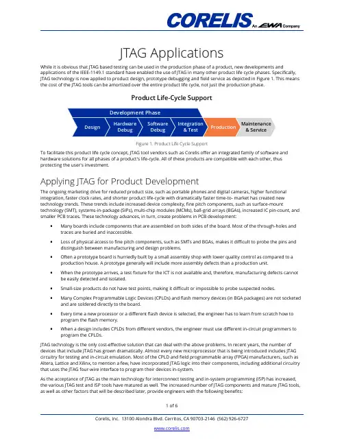
JTAG ApplicationsWhile it is obvious that JTAG based testing can be used in the production phase of a product, new developments and applications of the IEEE-1149.1 standard have enabled the use of JTAG in many other product life cycle phases. Specifically, JTAG technology is now applied to product design, prototype debugging and field service as depicted in Figure 1. This means the cost of the JTAG tools can be amortized over the entire product life cycle, not just the production phase.Product Life-Cycle SupportTo facilitate this product life cycle concept, JTAG tool vendors such as Corelis offer an integrated family of software and hardware solutions for all phases of a product's life-cycle. All of these products are compatible with each other, thus protecting the user's investment.Applying JTAG for Product DevelopmentThe ongoing marketing drive for reduced product size, such as portable phones and digital cameras, higher functional integration, faster clock rates, and shorter product life-cycle with dramatically faster time-to- market has created new technology trends. These trends include increased device complexity, fine pitch components, such as surface-mount technology (SMT), systems-in-package (SIPs), multi-chip modules (MCMs), ball-grid arrays (BGAs), increased IC pin-count, and smaller PCB traces. These technology advances, in turn, create problems in PCB development:∙Many boards include components that are assembled on both sides of the board. Most of the through-holes and traces are buried and inaccessible.∙Loss of physical access to fine pitch components, such as SMTs and BGAs, makes it difficult to probe the pins and distinguish between manufacturing and design problems.∙Often a prototype board is hurriedly built by a small assembly shop with lower quality control as compared to a production house. A prototype generally will include more assembly defects than a production unit.∙When the prototype arrives, a test fixture for the ICT is not available and, therefore, manufacturing defects cannot be easily detected and isolated.∙Small-size products do not have test points, making it difficult or impossible to probe suspected nodes.∙Many Complex Programmable Logic Devices (CPLDs) and flash memory devices (in BGA packages) are not socketed and are soldered directly to the board.∙Every time a new processor or a different flash device is selected, the engineer has to learn from scratch how to program the flash memory.∙When a design includes CPLDs from different vendors, the engineer must use different in-circuit programmers to program the CPLDs.JTAG technology is the only cost-effective solution that can deal with the above problems. In recent years, the number of devices that include JTAG has grown dramatically. Almost every new microprocessor that is being introduced includes JTAG circuitry for testing and in-circuit emulation. Most of the CPLD and field programmable array (FPGA) manufacturers, such as Altera, Lattice and Xilinx, to mention a few, have incorporated JTAG logic into their components, including additional circuitry that uses the JTAG four-wire interface to program their devices in-system.As the acceptance of JTAG as the main technology for interconnect testing and in-system programming (ISP) has increased, the various JTAG test and ISP tools have matured as well. The increased number of JTAG components and mature JTAG tools, as well as other factors that will be described later, provide engineers with the following benefits:∙ Easy to implement Design-For- Testability (DFT) rules. A list of basic DFT rules is provided later in this article. ∙ Design analysis prior to PCB layout to improve testability. ∙ Packaging problems are found prior to PCB layout. ∙ Little need for test points. ∙ No need for test fixtures.∙ More control over the test process.∙ Quick diagnosis (with high resolution) of interconnection problems without writing any functional test code. ∙ Program code in flash devices.∙ Design configuration data placement into CPLDs. ∙JTAG emulation and source-level debugging.What JTAG Tools are needed?In the previous section, we listed many of the benefits that a designer enjoys when incorporating boundary-scan in his product development. In this section we describe the tools and design data needed to develop JTAG test procedures and patterns for ISP, followed by a description of how to test and program a board. We use a typical board as an illustration for the various JTAG test functions needed. A block diagram of such a board is depicted in . A typical digital board with JTAG devices includes the following main components:∙ Various JTAG components such as CPLDs, FPGAs, Processors, etc., chained together via the boundary-scan path. ∙ Non-JTAG components (clusters). ∙ Various types of memory devices. ∙ Flash Memory components. ∙Transparent components such as series resistors or buffers.Most of the boundary-scan test systems are comprised of two basic elements: Test Program Generation and Test Execution. Generally, a Test Program Generator (TPG) requires the netlist of the Unit Under Test (UUT) and the BSDL files of the JTAG components. The TPG automatically generates test patterns that allow fault detection and isolation for all JTAG testable nets of the PCB. A good TPG can be used to create a thorough test pattern for a wide range of designs. For example, ScanExpress TPG typically achieves net coverage of more than 60%, even though the majority of the PCB designs are not optimized for boundary-scan testing. The TPG also creates test vectors to detect faults on the pins of non-scannable components, such as clusters and memories that are surrounded by scannable devices.Some TPGs also generate a test coverage report that allows the user to focus on the non-testable nets and determine whatadditional means are needed to increase the test coverage.I/O I/OFigure 2. Typical Board with JTAG ComponentsTest programs are generated in seconds. For example, when Corelis ScanExpress TPG™ was used, it took a 3.0 GHz Pentium 4 PC 23 seconds to generate aninterconnect test for a UUT with 5,638 nets (with 19,910 pins). This generation time includes netlist and all other input files processing as well as test pattern file generation.Test execution tools from various vendors provide means for executing JTAG tests and performing in-system programming in a pre-planned specific order, called a test plan. Test vectors files, which have been generated using the TPG, are automatically applied to the UUT and the results are compared to the expected values. In case of a detected fault, the systemdiagnoses the fault and lists the failures as depicted in Figure 3. Figure 3 shows the main window of the Corelis test execution tool, ScanExpress Runner™. ScanExpress Runner gives the user an overview of all test steps and the results of executed tests. Theseresults are displayed both for individual tests as well as for the total test runs executed. ScanExpress Runner provides the ability to add or delete various test steps from a test plan, or re-arrange the order of the test steps in a plan. Tests can also be enabled or disabledand the test execution can be stopped upon the failure of any particular test.Different test plans may be constructed for different UUTs. Tests within a test plan may be re-ordered, enabled or disabled, and unlimited different tests can be combined into a test plan. ScanExpress Runner can be used to develop a test sequence or test plan from various independent sub-tests. These sub-tests can then be executed sequentially as many times asspecified or continuously if desired. A sub-test can also program CPLDs and flash memories. For ISP, other formats, such as SVF, JAM, and STAPL, are also supported.To test the board depicted in Figure 2, the user must execute a test plan that consists of various test steps as shown in Figure 3.The first and most important test is the scan chain infrastructure integrity test. The scan chain must work correctly prior to proceeding to other tests and ISP. Following a successful test of the scan chain, the user can proceed to testing all the interconnectionsbetween the JTAG components. If the interconnect test fails, ScanExpress Runner displays a diagnostic screen that identifies the type of failure (such as stuck-at, Bridge, Open) and lists the failing nets and pins as shown in Figure 4. Once the interconnect test passes, including the testing of transparent components, it makes sense to continue testing the clusters and the memory devices. At this stage, the system is ready for in-system programming, which typically takes more time as compared to testing.Figure 3. ScanExpress Runner Main WindowFigure 4. ScanExpress Runner Diagnostics WindowDuring the design phase of a product, some JTAG vendors will provide design assistance in selecting JTAG-compliant components, work with the developers to ensure that the proper BSDL files are used, and provide advice in designing the product for testability.Applying JTAG for Production TestProduction testing, utilizing traditional In-Circuit Testers that do not have JTAG features installed, experience similar problems that the product developer had and more:∙Loss of physical access to fine pitch components, such as SMTs and BGAs, reduces bed-of-nails ICT fault isolation.∙Development of test fixtures for ICTs becomes longer and more expensive.∙Development of test procedures for ICTs becomes longer and more expensive due to more complex ICs.∙Designers are forced to bring out a large number of test points, which is in direct conflict with the goal to miniaturize the design.∙In-system programming is inherently slow, inefficient, and expensive if done with an ICT.∙Assembling boards with BGAs is difficult and subject to numerous defects, such as solder smearing. JTAG Embedded Functional TestRecently, a test methodology has been developed which combines the ease-of-use and low cost of boundary-scan with the coverage and security of traditional functional testing. This new technique, called JTAG Emulation Test (JET), lets engineers automatically develop PCB functional test that can be run at full speed., If the PCB has an on-board processor with a JTAG port (common, even if the processor doesn't support boundary-scan), JET and boundary-scan tests can be executed as part of the same test plan to provide extended fault coverage to further complement or replace ICT testing.Corelis ScanExpress JET™ provides JTAG embedded test for a wide range of processors. For more information about this technology and product, visit the ScanExpress JET product page.Production Test FlowFigure 5 shows different production flow configurations. The diagram shows two typical ways that JTAG is deployed:∙As a stand-alone application at a separate test station or testbench to test all theinterconnects and perform ISPof on-board flash and othermemories. JTAG embeddedfunctional test (JET) may beintegrated with boundary-scan.∙Integrated into the ICT system,where the JTAG controlhardware is embedded in theICT system and the boundary-scan (and possibly JET) softwareis a module called from the ICTsoftware system.In the first two cases, the test flow is sometimes augmented with a separate ICT stage after the JTAG-based testing is completed, although it is becoming more common for ICT to be skipped altogether or at least to be limited to analog or special purpose functional testing.Figure 5. Typical Production FlowsThe following are major benefits in using JTAG test and in-system programming in production:∙No need for test fixtures.∙Integrates product development, production test, and device programming in one tool/system.∙Engineering test and programming data is reused in Production.∙Fast test procedure development.∙Preproduction testing can start the next day when prototype is released to production.∙Dramatically reduces inventory management – no pre-programmed parts eliminates device handling and ESD damage.∙Eliminates or reduces ICT usage time – programming and screening.Production test is an obvious area in which the use of boundary-scan yields tremendous returns. Automatic test program generation and fault diagnostics using JTAG software products and the lack of expensive fixturing requirements can make the entire test process very economical. For products that contain edge connectors and digital interfaces that are not visible from the boundary-scan chain, JTAG vendors offer a family of boundary-scan controllable I/Os that provide a low cost alternative to expensive digital pin electronics.Field Service and InstallationThe role of JTAG does not end when a product ships. Periodic software and hardware updates can be performed remotely using the boundary-scan chain as a non-intrusive access mechanism. This allows flash updates and reprogramming of programmable logic, for example. Service centers that normally would not want to invest in special equipment to support a product now have an option of using a standard PC or laptop for JTAG testing. A simple PC-based JTAG controller can be used for all of the above tasks and also double as a fault diagnostic system, using the same test vectors that were developed during the design and production phase. This concept can be taken one step further by allowing an embedded processor access to the boundary-scan chain. This allows diagnostics and fault isolation to be performed by the embedded processor. The same diagnostic routines can be run as part of a power-on self-test procedure.JTAG Design-for-Test Basic ConsiderationsAs mentioned earlier in this article, the design for JTAG test guidelines are simple to understand and follow compared to other traditional test requirements. It is important to remember that JTAG testing is most successful when the design and test engineering teams work together to ensure that testability is "designed in" from the start. The boundary-scan chain is the most critical part of JTAG implementations. When that is properly implemented, improved testability inevitably follows. Below is a list of basic guidelines to observe when designing a JTAG-testable board:∙If there are programmable components in a chain, such as FPGAs, CPLDs, etc., group them together in the chain order and place the group at either end of the chain. It is recommended that you provide access to Test Data In(TDI) and Test Data Out (TDO) signals where the programmable group connects to the non-programmable devices.∙All parts in the boundary-scan chain should have 1149.1-compliant test access ports (TAPs).∙Use simple buffering for the Test Clock (TCK) and Test Mode Select (TMS) signals to simplify test considerations for the boundary-scan TAP. The TAP signals should be buffered to prevent clocking and drive problems.∙Group similar device families and have a single level converter interface between them, TCK, TMS, TDI, TDO, and system pins.∙TCK should be properly routed to prevent skew and noise problems.∙Use the standard JTAG connector on your board as depicted in Corelis documentation.∙Ensure that BSDL files are available for each JTAG component that is used on your board and that the files are validated.Design for interconnect testing requires board-level system understanding to ensure higher test coverage and elimination of signal level conflicts.∙Determine which JTAG components are on the board. Change as many non-JTAG components to IEEE 1149.1-compliant devices as possible in order to maximize test coverage.∙Check non-JTAG devices on the board and design disabling methods for the outputs of those devices in order to prevent signal level conflicts. Connect the enable pins of the conflicting devices to JTAG controllable outputs. Corelis tools will keep the enable/disable outputs at a fixed disabling value during the entire test.∙Ensure that your memory devices are surrounded by JTAG components. This will allow you to use a test program generator, such as ScanExpress TPG, to test the interconnects of the memory devices.∙Check the access to the non-boundary-scan clusters. Make sure that the clusters are surrounded by JTAG components. By surrounding the non-boundary-scan clusters with JTAG devices, the clusters can then be testedusing a JTAG test tool.∙If your design includes transparent components, such as series resistors or non-inverting buffers, your test coverage can be increased by testing through these components using ScanExpress TPG.∙Connect all I/Os to JTAG controllable devices. This will enable the use of JTAG, digital I/O module, such as the ScanIO-300LV, to test all your I/O pins, thus increasing test coverage.。

专业英语--电力电子方面AbsorberCircuit汲取电路AC/ACFrequencyConverter交交变频电路ACpowercontrol交流电力操纵ACPowerController交流调功电路ACPowerElectronicSwitch交流电力电子开关AcV oltageController交流调压电路AsynchronousModulation异步调制BakerClampingCircuit贝克箝位电路Bi-directionalTriodeThyristor双向晶闸管BipolarJunctionTransistor--BJT双极结型晶体管Boost-BuckChopper升落压斩波电路BoostChopper升压斩波电路BoostConverter升压变换器BridgeReversibleChopper桥式可逆斩波电路BuckChopper落压斩波电路BuckConverter落压变换器Commutation换流ConductionAngle导通角ConstantV oltageConstantFrequency--CVCF恒压恒频ContinuousConduction--CCM〔电流〕连续模式ControlCircuit操纵电路CukCircuitCUK斩波电路CurrentReversibleChopper电流可逆斩波电路CurrentSourceTypeInverter--CSTI电流〔源〕型逆变电路Cycloconvertor周波变流器DC-AC-DCConverter直交直电路DCChopping直流斩波DCChoppingCircuit直流斩波电路DC-DCConverter直流-直流变换器DeviceCommutation器件换流DirectCurrentControl直截了当电流操纵DiscontinuousConductionmode〔电流〕断续模式displacementfactor位移因数printedcircuit印制电路printedwiring印制线路printedboard印制板printedcircuitboard印制板电路printedwiringboard印制线路板printedcomponent印制元件printedcontact印制接点printedboardassembly印制板装配board板rigidprintedboard刚性印制板flexibleprintedcircuit挠性印制电路flexibleprintedwiring挠性印制线路flushprintedboard齐平印制板metalcoreprintedboard金属芯印制板metalbaseprintedboard金属基印制板mulit-wiringprintedboard多重布线印制板moldedcircuitboard模塑电路板discretewiringboard散线印制板microwireboard微线印制板buile-upprintedboard积层印制板surfacelaminarcircuit外表层合电路板B2itprintedboard埋进凸块连印制板chiponboard载芯片板buriedresistanceboard埋电阻板motherboard母板daughterboard子板backplane背板bareboard裸板copper-invar-copperboard键盘板夹心板dynamicflexboard动态挠性板staticflexboard静态挠性板break-awayplanel可断拼板cable电缆flexibleflatcable(FFC)挠性扁平电缆membraneswitch薄膜开关hybridcircuit混合电路thickfilm厚膜thickfilmcircuit厚膜电路thinfilm薄膜thinfilmhybridcircuit薄膜混合电路interconnection互连conductortraceline导线flushconductor齐平导线transmissionline传输线crossover跨交edge-boardcontact板边插头stiffener增强板substrate基底realestate基板面conductorside导线面componentside元件面solderside焊接面printing印制grid网格pattern图形conductivepattern导电图形non-conductivepattern非导电图形legend字符mark标志basematerial基材laminate层压板metal-cladbadematerial覆金属箔基材copper-cladlaminate(CCL)覆铜箔层压板compositelaminate复合层压板thinlaminate薄层压板basismaterial基体材料prepreg预浸材料bondingsheet粘结片preimpregnatedbondingsheer预浸粘结片epoxyglasssubstrate环氧玻璃基板masslaminationpanel预制内层覆箔板corematerial内层芯板bondinglayer粘结层filmadhesive粘结膜unsupportedadhesivefilm无支撑胶粘剂膜coverlayer(coverlay)覆盖层stiffenermaterial增强板材copper-cladsurface铜箔面foilremovalsurface往铜箔面uncladlaminatesurface层压板面basefilmsurface基膜面adhesivefaec胶粘剂面platefinish原始光洁面mattfinish粗面lengthwisedirection纵向crosswisedirection模向cuttosizepanel剪切板ultrathinlaminate超薄型层压板A-stageresinA阶树脂B-stageresinB阶树脂C-stageresinC阶树脂epoxyresin环氧树脂phenolicresin酚醛树脂polyesterresin聚酯树脂polyimideresin聚酰亚胺树脂bismaleimide-triazineresin双马来酰亚胺三嗪树脂acrylicresin丙烯酸树脂melamineformaldehyderesin三聚氰胺甲醛树脂polyfunctionalepoxyresin多官能环氧树脂brominatedepoxyresin溴化环氧树脂epoxynovolac环氧酚醛fluroresin氟树脂siliconeresin硅树脂silane硅烷polymer聚合物amorphouspolymer无定形聚合物crystallinepolamer结晶现象dimorphism双晶现象copolymer共聚物synthetic合成树脂thermosettingresin热固性树脂thermoplasticresin热塑性树脂photosensitiveresin感光性树脂epoxyvalue环氧值dicyandiamide双氰胺binder粘结剂adesive胶粘剂curingagent固化剂flameretardant阻燃剂opaquer遮光剂plasticizers增塑剂unsatuiatedpolyester不饱和聚酯polyester聚酯薄膜polyimidefilm(PI)聚酰亚胺薄膜polytetrafluoetylene(PTFE)聚四氟乙烯reinforcingmaterial增强材料glassfiber玻璃纤维E-glassfibreE玻璃纤维D-glassfibreD玻璃纤维S-glassfibreS玻璃纤维glassfabric玻璃布non-wovenfabric非织布glassmats玻璃纤维垫yarn纱线filament单丝strand绞股weftyarn纬纱warpyarn经纱denier但尼尔warp-wise经向threadcount织物经纬密度weavestructure织物组织plainstructure平纹组织greyfabric坏布wovenscrim稀松织物bowofweave弓纬endmissing断经mis-picks缺纬bias纬歪crease折痕waviness云织fisheye鱼眼featherlength毛圈长mark厚薄段split裂缝twistofyarn捻度sizecontent浸润剂含量sizeresidue浸润剂残留量finishlevel处理剂含量size浸润剂couplintagent偶联剂finishedfabric处理织物polyarmidefiber聚酰胺纤维aromaticpolyamidepaper聚芳酰胺纤维纸breakinglength断裂长heightofcapillaryrise吸水高度wetstrengthretention湿强度保持率whitenness白度ceramics陶瓷conductivefoil导电箔copperfoil铜箔rolledcopperfoil压延铜箔annealedcopperfoil退火铜箔thincopperfoil薄铜箔adhesivecoatedfoil涂胶铜箔resincoatedcopperfoil涂胶脂铜箔compositemetallicmaterial复合金属箔carrierfoil载体箔invar殷瓦foilprofile箔〔剖面〕轮廓shinyside光面matteside粗糙面treatedside处理面stainproofing防锈处理doubletreatedfoil双面处理铜箔shematicdiagram原理图logicdiagram逻辑图printedwirelayout印制线路布设masterdrawing布设总图computeraideddrawing计算机辅助制图computercontrolleddisplay计算机操纵显示placement布局routing布线layout布图设计rerouting重布simulation模拟logicsimulation逻辑模拟circitsimulation电路模拟timingsimulation时序模拟modularization模块化layouteffeciency布线完成率MDFdatabse机器描述格式数据库designdatabase设计数据库designorigin设计原点optimization(design)优化〔设计〕predominantaxis供设计优化坐标轴tableorigin表格原点mirroring镜像drivefile驱动文件intermediatefile中间文件manufacturingdocumentation制造文件queuesupportdatabase队列支撑数据库componentpositioning元件安置graphicsdispaly图形显示scalingfactor比例因子scanfilling扫描填充rectanglefilling矩形填充regionfilling填充域physicaldesign实体设计logicdesign逻辑设计logiccircuit逻辑电路hierarchicaldesign层次设计top-downdesign自顶向下设计bottom-updesign自底向上设计net线网digitzing数字化designrulechecking设计规那么检查router(CAD)走〔布〕线器netlist网络表subnet子线网objectivefunction目标函数postdesignprocessing(PDP)设计后处理interactivedrawingdesign交互式制图设计costmetrix费用矩阵engineeringdrawing工程图blockdiagram方块框图moze迷宫componentdensity元件密度travelingsalesmanproblem回售货员咨询题degreesfreedom自由度outgoingdegree进度incomingdegree出度manhattondistance曼哈顿距离euclideandistance欧几里德距离network网络array阵列segment段logic逻辑logicdesignautomation逻辑设计自动化separatedtime分线separatedlayer分层definitesequence定顺序conduction(track)导线〔通道〕conductorwidth导线〔体〕宽度conductorspacing导线距离conductorlayer导线层conductorline/space导线宽度/间距conductorlayerNo.1第一导线层roundpad圆形盘squarepad方形盘diamondpad菱形盘oblongpad长方形焊盘bulletpad子弹形盘teardroppad泪滴盘snowmanpad雪人盘V-shapedpadV形盘annularpad环形盘non-circularpad非圆形盘isolationpad隔离盘monfunctionalpad非功能连接盘offsetland偏置连接盘back-bardland腹〔背〕裸盘anchoringspaur盘址landpattern连接盘图形landgridarray连接盘网格阵列annularring孔环componenthole元件孔mountinghole安装孔supportedhole支撑孔unsupportedhole非支撑孔via导通孔platedthroughhole(PTH)镀通孔accesshole余隙孔blindvia(hole)盲孔buriedviahole埋孔buriedblindvia埋,盲孔anylayerinnerviahole任意层内部导通孔alldrilledhole全部钻孔toalinghole定位孔landlesshole无连接盘孔interstitialhole中间孔landlessviahole无连接盘导通孔pilothole引导孔terminalclearomeehole端接全隙孔dimensionedhole准尺寸孔via-in-pad在连接盘中导通孔holelocation孔位holedensity孔密度holepattern孔图drilldrawing钻孔图assemblydrawing装配图datumreferan参考基准1〕元件设备三绕组变压器:three-columntransformerThrClnTrans双绕组变压器:double-columntransformerDblClmnTrans 电容器:Capacitor并联电容器:shuntcapacitor电抗器:Reactor母线:Busbar输电线:TransmissionLine发电厂:powerplant断路器:Breaker刀闸(隔离开关):Isolator分接头:tap电动机:motor〔2〕状态参数有功:activepower无功:reactivepower电流:current容量:capacity电压:voltage档位:tapposition有功损耗:reactiveloss无功损耗:activeloss功率因数:power-factor功率:power功角:power-angle电压等级:voltagegrade空载损耗:no-loadloss铁损:ironloss铜损:copperloss空载电流:no-loadcurrent阻抗:impedance正序阻抗:positivesequenceimpedance负序阻抗:negativesequenceimpedance零序阻抗:zerosequenceimpedance电阻:resistor电抗:reactance电导:conductance电纳:susceptance无功负载:reactiveload或者QLoad有功负载:activeloadPLoad远测:YC(telemetering)远信:YX励磁电流(转子电流):magnetizingcurrent定子:stator功角:power-angle上限:upperlimit下限:lowerlimit并列的:apposable高压:highvoltage低压:lowvoltage中压:middlevoltage电力系统powersystem发电机generator励磁excitation励磁器excitor电压voltage电流current母线bus变压器transformer升压变压器step-uptransformer高压侧highside输电系统powertransmissionsystem输电线transmissionline固定串联电容补偿fixedseriescapacitorcompensation 稳定stability电压稳定voltagestability功角稳定anglestability暂态稳定transientstability电厂powerplant能量输送powertransfer交流AC装机容量installedcapacity电网powersystem落点droppoint开关站switchstation双回同杆并架double-circuitlinesonthesametower 变电站transformersubstation补偿度degreeofcompensation高抗highvoltageshuntreactor无功补偿reactivepowercompensation故障fault调节regulation裕度magin三相故障threephasefault故障切除时刻faultclearingtime极限切除时刻criticalclearingtime切机generatortriping高顶值highlimitedvalue强行励磁reinforcedexcitation线路补偿器LDC(linedropcompensation)机端generatorterminal静态static(state)动态dynamic(state)单机无穷大系统onemachine-infinitybussystem 机端电压操纵A VR电抗reactance电阻resistance功角powerangle有功〔功率〕activepower无功〔功率〕reactivepower功率因数powerfactor无功电流reactivecurrent下落特性droopcharacteristics歪率slope额定rating变比ratio参考值referencevalue电压互感器PT分接头tap下落率drooprate仿真分析simulationanalysis传递函数transferfunction框图blockdiagram受端receive-side裕度margin同步synchronization失往同步lossofsynchronization阻尼damping摇摆swing保卫断路器circuitbreaker电阻:resistance电抗:reactance阻抗:impedance电导:conductance电纳:susceptance导纳:admittance电感:inductance电容:capacitance金属化聚丙烯膜电容\metallizationpolypropylenefilmcapacitor\插件磁芯电感\magneticcoreinductance\涤纶电容\terylenecapacity\接地片\groundlug\碳膜电阻\carbonfilmresistor\瓷片电容\ceramicdisccapacitor\莲花插座\lotussocket\贴片磁珠\coatedmageticbead贴片三极管\coateddynatron话题:专业词汇1backplane背板2Bandgapvoltagereference带隙电压参考3benchtopsupply工作台电源4BlockDiagram方块图5BodePlot波特图6Bootstrap自举7BottomFETBottomFET8bucketcapcitor桶形电容9chassis机架10Combi-senseCombi-sense11constantcurrentsource恒流源12CoreSataration铁芯饱和13crossoverfrequency交叉频率14currentripple纹波电流15CyclebyCycle逐周期16cycleskipping周期跳步17DeadTime死区时刻18DIETemperature核心温度19Disable非使能,无效,禁用,关断20dominantpole主极点21Enable使能,有效,启用22ESDRatingESD额定值23EvaluationBoard评估板24Exceedingthespecificationsbelowmayresultinpermanentdamagetothedevice,ordevicemalfunctio n.OperationoutsideoftheparametersspecifiedintheElectricalCharacteristicssectionisnotimplied.超过下面的规格使用可能引起永久的设备损害或设备故障。

专利名称:PERFORMANCE-AWARE AND RELIABILITY-AWARE DATA PLACEMENT FOR N-LEVELHETEROGENEOUS MEMORY SYSTEMS发明人:Manish Gupta,David A. Roberts,Mitesh R.Meswani,Vilas Sridharan,StevenRaasch,Daniel I. Lowell申请号:US15331270申请日:20161021公开号:US20170277441A1公开日:20170928专利内容由知识产权出版社提供专利附图:摘要:Techniques for selecting one of a plurality of heterogeneous memory units for placement of blocks of data (e.g., memory pages), based on both reliability and performance, are disclosed. A “cost” for each data block/memory unit combination is determined, based on the frequency of access of the data block, the latency of the memory unit, and, optionally, an architectural vulnerability factor (which represents the level of exposure of a particular memory data value to memory faults such as bit flips). A memory unit is selected for the data block for which the determined cost is the lowest, out of all memory units considered, and the data block is placed into that memory unit.申请人:Advanced Micro Devices, Inc.地址:Sunnyvale CA US国籍:US更多信息请下载全文后查看。

[检索词汇] altium designer 中英文技术词汇对照PCB AD常用术语翻译对译protel 单词Accept 接受Accuracy 精确度准确度Activate 激活活动启动Add 添加Address 地址Advance 高级Aide 助手辅助Align 排列对齐Alpha 开端Analog 模拟的Analyzer 分析器测定仪Angle 角度观点Annotate 注解Aperture 孔径光圈Applocation 应用程序Approximation 接近近似值Arc 圆弧弧度Architectur结构体构造Array 阵列数组Ascend 登高上升Assembly 集合装配Associate关联的辅助的Asynchronous 异步的Automatical 自动的Access 存取通道接近Action 行动作用Active 积极的活泼的Adder 加法器Administration 管理员管理器Aggressor 干扰源入侵者Alias 别名化名混淆Allow 允许Always 总是永远Analysis 分析研究Animation 动画Any 任意的Applicable 可应用的适用的Apply 应用Arbiter 仲裁器Architect 设计者制造者Area 面积范围Arrange安排排列调整Arrow 箭形Assembler 装配器汇编Assign 分配分派指定Astable 非稳态的多谐振荡的Attempt 尝试Available 有效的有用的Backup 备用Bar 标签Base 基极基础基地Batch 批处理批量Begin 开始创建Behavior 行为举止态度Bell 铃钟Between 两者之间Bidir 允许双向Bidirectional 双向性Bill 清单Binary 二进制二元的Bistable 双稳Bit 位Bitmap 位图Black 黑色黑色的Blind 盲孔Blip 标志信号Block 框栏隔阻Board 板子牌子委员会Body 物体主干主体Boolean 布尔值Border 边线Bottom 底部Bounce 反弹抖动Breakpoint 中断点断点Broken 破裂的损坏的Browse 浏览Buffer 缓冲器Build 构建Bullet 锥形体Bury 埋藏Bus 总线Butterfly 蝶形Button 按钮Bypass 省略Byte 字节Cable 电缆Calculation 计算估计CAM(computer aided manufacturing)计算机辅助制造Cancel 作废删除Capacitor 电容Caption 标题Capture 捕获收集记录Case 实情案例Category 类目范畴部属Cathode 阴极Center 中心Centimeter 厘米Chain 链Change 改变Channel 通道Charge 充电指责指示Check 检测Chart 制成图表Child 子女Chip 集成芯片Circuit 电路Circular 圆环弧形Class 阶层等级Cleanup 清扫工作Clear 清除清零Clearance 清除余地间隙Click 单击点击Clipboard 剪切板Clock 时钟Close 关闭结束Closure 关闭闭幕Code 编码代码Collector 集电极Color 彩色着色Colour 颜色Column 圆柱纵列栏目Combination 组合Comma 逗号Command 命令Comparator 比较器Community 社区群落Compilation 编辑物Compatible 兼容的和谐的Component 元器件组成成分Compile 编辑收集汇编Computer 计算机Composite 合成的复合的综合的Condition 条件Concurrent 并发事件同行Configure 配置Confidence 置信度自信信赖Conflict 冲突Confirm 确认证实Connector 连接端Connectivity 连线Constraint 约束限制因素Console 主控台表盘托架Consumer 用户使用者Construction 构造Continue 继续延伸Contract 缩短Control 控制Convert 转化转变Coordinate 坐标Copper 铜Copy 拷贝复制Core 核Cord 绳线索Corner 角落拐角Corporation 公司企业法人Counter 计数器Courtyard 天井庭院Create 创建Cross 十字符号混合Crosspoint 插入测试点Crosstalk 串扰CRTCrystal 晶体Current 电流当前的流行的Cursor 光标游标指示器Custom 惯例Customer 用户客户Cutout 切出划出挖空Cycle 周期Comment 注释发表评论说明书Dashed 下划线Data 数字数据Databse 数据库资料库Date 日期Daughtrer 子系子插件派生Debug 排错调试Dead 死的Decimal 十进制小数Decade 十进制十年Default 默认值缺省值弃权Decoder 译码器Definition 定义式限定分辨率Define 定义下定义Delay 延时Degree 度等级Demo 演绎演示版Delete 删除Demote 降级降低Deny 否认Description 描述Designator 标识指示者Designer 设计师Destination 目标目的Detail 细节零件Device 装置设备图样器件Diagram 示意图Dialog 对话Diagonal 对角线Difference 差异查分差额Diamond 菱形钻石Digital 数字的Different 不同的Dimension 尺度Dim 朦胧暗淡Direct 指示指令Diode 二极管Disable 无能无效无用Director 指南指导咨询Disk 圆盘Discharge 放点排出释放Distribution 分配分布分发Display 显示Dock 停放连接接驳Divider 分配分割Dot 小点虚线点缀Donut 环形Download 下载Down 下降Draw 绘制描写冲压成型Drag 拖拽Drop 下拉滴落遗漏Drill 钻Duplicate 复制副本Dual 双数的两倍Duty 占空比Edge 边缘Edit 编辑Efficient 高效的有能力的Electrical 电气的电学的电力的Ellipse 椭圆Embed 潜入插入Emitter 射极Emulate 效法Enable 使能激活有效Encoder 编码器End 结束Engineer 设计建造工程师Enter 进入参加Entity 实体Entry 入口Enum 列举型别Error 错误Evaluation 评价评估鉴定Example 例子Excel 胜过优秀突出Execute 执行实施签署Exist 存在的现有的Expand 扩大推广展开Expansion 扩大扩展扩张Expiry 终止期满Explode 爆炸分解Exponent 指数Export 输出出品Explore 探究查询Extra 额外的附加的External 外部的外面的外形Extrude 压制突出Extract 提取摘录Fabrication 制造Frequency 频率Failure 无效毁坏的Function 函数功能False 虚假的伪造的Fail 失败不足Fanout 扇出Fall 下降降落落差Favorite 最爱的(sthsb)Famale 凹的阴的Figure 图形Fatal 致命的Fill 填充Field 现场域范围Filter 过滤器File 文件Find 建立发现Film 胶片First 第一首先Finally 最终的Flash 闪光闪烁曝光Finish 完成结束Flatten 弄平弄直Fit 适合相配Flip-flop 触发器Flat 平的平坦的Floorplan 层平面图Flip 倒转Focus 集中聚焦Float 发行Footprint 封装Flow 流动源自Format 格式Folder 文件夹折叠Formula 公式Force 强制FPGAForum 讨论论坛会Frame 框图塑造Free 自由Framework 架构结构Form 从··起由于Gate 门Generate 产生导致造成Graphic 图形green 绿色Grid 栅格Ground 地面基础Group 组类集聚Guide 引导指南手册Hard 坚硬的困难的Hardware 硬件设备五金Harmonic 谐波谐振Harness 束Hatch 策划画影线舱口Hazard 冒险Hazy 模糊的混浊的Height 高度Help 帮助Hexadecimal 十六进制Hide 隐藏Hierarchy 体系分层系列High 高的高级的高尚的Hint 暗示History 历史记录Horizontal 水平横向Hug 拥抱紧靠Ideal 理想的Identical 相同的相等的恒等的Identifier 识别符Identify 识别标记IDF(integrated data file) 综合资料文件IEEE 电气电子工程师协会Impedance 阻抗Ignore 忽略Import 输入导入Imperial 英制的Include 包含Incident 事变入射Index 索引Increment 增量Inductor 电感Indication 指示表示Information 信息Industry 工业企业产业行业Innovation 创新Initial 最初的开始的Insert 插入嵌入添Input 输入Insight 洞察顿悟Inside 内部的里面的Install 安装Inspector 检查视察Instrument 仪器Instance 实例Integrate 积分的集成使完成使结合Integer 整数Interactive 互动的交互的Integrity 完整的Interface 接口界面Interconnect 互联器Internet 因特网Internal 内部的IPC(industry processcontrol)工业过程控制Interrupt 打断中断Isolate 隔离Island 孤岛岛屿Item 项目条款ISP(In-systemprogrammable)在线编程JTAG(joint test actiongroup) 联合测试行为组Job 工作职业Joint 联合的Jump 跳跃Junctions 结点接点Keep 保持Key 关键钥匙Kind 种类Knowledge 知识Label 标签商标Lattice 晶格点阵Landscape 横向Layer 层Latch 锁存器锁扣LCD(liquid crystaldisplay) 液晶显示器Launch 发射投掷出版LED(light emitting diode)发光二级管Layout 布置布局Legacy 老化遗留下Learn 学习学会认知Length 长度Left 左边向左Less 较少的Legend 图例图注Library 库图书馆Lens 镜Line 线条线路Level 水平Link 链接连接License 注册Linear 线性的直线的一次的Liquid 液体流体不稳的Live 激活Localize 本地局部本地化定位Locate 把··设置在位置场所Lock 锁定Log 记录Logarithmic 对数的Logic 逻辑逻辑学Logical 逻辑的合理的Login 登录Lookup 查找查阅Loop 循环环状物Low 低的矮的Lot 地段许多Laboratory 实验室LPM(library of parameter modules) 参数化模块库Language 语言用语术语Machine 机器机械Multivibrator 多谐振荡器Maker 制造者Magnitude 幅值强度量值Manage 管理操纵Male 阳的Manual 手册手动的Manager 管理者经理主任Map 图Manufacture 制造制作加工Match 匹配比赛Mask 表面掩膜屏蔽Matrix 矩阵混合物Material 材料物质Maximum 最大值最大量Maximize 增加扩大Measure 测量Meal 粉状物膳食Medium 中间的媒介Mechanical 机械的Membership 会员资格Mega 许多非常强大Memory 存储器内存Menu 菜单Merge 合并Message 信息Meter 米(长度单位)Metric 公制的Microsoft 微软Millimeter 毫米Minimum 最小值Miscellaneous 混合杂项多样Miser 钻探机Miss 损失差错遗漏Miter 斜接斜角Mix 混合结合杂交Mode 形状方式风格Model 模型模特型号Modify 更改修饰Module 模块组件单元Moire 网纹纹波龟纹Mold 模块模型Monitor 监控Monostable 单稳状态Moor 固定系住Mount 安装Move 移动Mult 多种多元多路Magnify 放大Name 名称Nano 十亿分之一纳Navigator 领航导航Neck 领口瓶颈Negative 负的Net 网络Netlable 网络标号Netlist 网络表New 新的Next 下一步再Nexus 关系Node 结点波峰Noise 噪音None 忽略一个也没Normal 正常的常规的Number 数字号码数量Object 物体目标Octagon 八边形Octal 八进制Octave 八行八度八位ODBC(ovject database connectivity) 开放数据库互联Ohm 欧姆(电阻单位)OLE DB(object lin king and embedding databse) 目标链接及嵌入式数据库Online 在线Opcode 运算码Openbus 开放总线公共总线Open 开放的公开的Operate 工作运转营业Operand 操作数运算域Optimizer 优化程序优化器Operator 运算符Orange 橙子桔子Option 选择选项Orientation 取向Order 顺序Original 原本的最初的Origin 起源原点Outline 外形略述概括Orthogonal 直角的正交的Outside 外部的外观Output 输出Overlay 覆盖层Overall 全部的Owner 物主所有者Overshoot 过冲Package 封装包装Pad 焊盘基座垫料Page 页码翻阅Pair 成对成双Palette 调色盘选盘控制板Panel 面板画板嵌镶板Parallel 并行并联Parameter 参数系数因数Parent 父系Parsing 部析Part 部件Passive 无源的被动的Paste 助焊贴敷铜Path 路径轨迹PCBPeak 峰值Peripheral 周边的外围的Permission 同意Persistent 坚持不懈固执的Physical 物理的Pickbox 点选框取景框Pickup 拾取收集Pin 引脚管脚Place 放置Placement 布局Plane 平板平面飞机Plugin 插件栓Point 点Plus 十字记号加号Polygon 多边形多角形Pole 极极地Popup 弹出Polyline 折线Portable 可移植的移动的Port 端口Position 位置Portrait 竖向纵向Postpone 延时搁置Positive 正的Power 电源功率Pour 倾泻倒灌Preference 偏好优先Predefined 预先定义Preliminary 预备的初步语言的Prefix 前缀字首Preserve 保护保藏维护Prepreg 预浸料半固化品Preview 预览预习排练Preset 置数Primary 主要的Previous 以前的早先的Print 打印Primitive 原始的纯朴的Priority 优先级优先权Printout 打印输出Process 进程步骤Probe 探测调查Profile 外形轮廓部面Processor 处理器加工者Program 程序设计Programmable 可编程的Project 工程项目Proper 适当的恰当的Promote 促进创办Provider 提供者供应商Property 性质特性Pull 拉牵拖PSD(programmable system device) 可编程的系统部件Pulse 脉冲跳动Pullback 障碍阻扰拉回Push 推挤推进拓展Quality 质量特性Query 疑问质问问号Quiet 静态的安静的Radix 根基数RAMRange 级别排行类别Raster 光栅屏面Ray 射线光线闪现Rebuild 重建重构Recent 最近的Record 记录经历Rectangle 矩形长方形Rectangular 矩形的成直角的Red 红色的Reference 参考基准Reflect 反射Region 区域地带Register 寄存器Remove 删除移除Repeat 重复Report 报告Require 需要需求Reserve 储备保存Reset 复位置零Reshape 改造矫形变形Resistance 电阻值Resistor 店主Resource 资源Restore 恢复还原返回Restrict 限制约束Result 结果导致Retrieve 取回恢复Revision 修订本校正版Right 右的右方Ring 铃声环形物Rise 上升起立增强ROMRoom 房间空间位置Root 根根源本质Rotation 旋转自转Round圆的Routing 走线布线Row 成形排列Rule 规则Run 运转流行的趋势Server 服务服务器Same 相同的同样的Sans 没有无Save 保存Scalar 标量数量Scale 刻度调节Schematic 图表示意图Scope 范围域Score 成绩计分Script 脚本Scroll 卷动Search 搜索Secondary 次要的从属的Section 部分片断Seed 原因种子Select 挑选选拔Separate 分离区别标识Sequential 有顺序的相继的Serial 串行的系列的序列的Serif 细体字Series 串联连贯成套Session 学期期间Service 服务检修劳务Shader 材质Set 设置置位Shadow 阴影着色Shape 造型形状Share 共享Sheet 图纸方块Shelve 搁置暂缓考虑Shift 移动变换Shortcut 快捷方式Show 显示展示Signal 信号Sign 签署有符号的征兆标志Silent 沉默的Silkscreen 丝印层Similar 相似的类似的Simple 简单的朴实的Simulation 仿真Sitemap 网站地图网站导航Situs 地点位置Silce 切片薄片Slider 滑块滑动Slot 槽Small 小的细的微的Smart 智慧灵气Snap 跳转突然折断Snippet 片断摘录Software 软件Solder 焊接Solid 实心的固体的坚固的Sort 分类Source 电源根源Space 间隔间隙Speaker 扬声器Special 特殊的Specification 说明书明细表Specify 具体指定详细指明列入清单Speed 速度Split 分离Spreadsheet 电子表格试算表Square 方形正直的Stack 堆积层叠Standalone 单板机Standard 标准规范Standoff 支架平淡Start 起始Starve 不足饥饿State 状态形势州Static 静止的Station 平台地位Status 地位资格身份Step 步进踏步步骤Stimulus 激励促进刺激Stop 停止Storage 储存器Strategy 策略方案战略String 字符串串条弦Structure 构成结构组织Style 风格文体作风Subversion 颠覆Summary 摘要概括总结Support 支持Suppress 压制抑制阻止Surface 表面Suspend 暂停挂起终止Swap 交换Sweep 扫描环视Switch 开关Symbol 符号Synchronous 同步的Syntax 语法Synthesis 综合合成System 系统Table 表格True 真实Target 目标对象指标Tail 末尾尾部Technology 技术工艺Teardrop 泪滴Template 样板Temperature 温度气温Terminal 极限的末端的端子Tenting 掩盖遮掩Terminator 终端负载Terminate 终结终止Text 文本正本Test 测试Themselves 他们自己TFT 触摸屏显示器Thruhole 通孔Thermal 热的热量的Time 时间Tile 铺排Timer 定时器Timebase 时基Toggle 切换开关双稳Timing 时序定时Tool 工具Tolerance 公差容限容差Top 顶部Toolbar 工具栏工具条Total 总体的合计为Topic 题目Track 轨迹Touchscreen 触摸屏Train 培训Trail 拖Transfer 传递Trance 恍惚Transistor 三极管晶体管Transient 暂态瞬态Transparency 透明度Translate 转变翻译Triangle 三角Transport 传输Trigonometry 三角法Trigger 触发器启动引起Tube 真空管电子管试管Tune 调谐曲调协调Tutorial 指导导师Type 类型Unassign 未定义Uncouple 解耦松开Undershoot 下冲负尖峰Undo 取消还原Uniform 相同的一致的单调的Unique 独特的唯一的Unit 单位Universal 普遍的全体的宇宙的Unspecified 不规定不确定Up 向上Update 更新Usage 用法习惯处理Utility 实用的通用的Use 实用Valid 有效的确实的合法的Validate 使生效Validation 确认验证Value 数值价值价格评价Variant 变化派生Vector 矢量向量Vendor 供应商卖主Version 版本翻译Vertical 垂直纵向Vertex 顶点制高点极点Very 很非常甚至VHDLVia 经由过孔Victim 被干扰受害者Video 视频录像View 查看Violation 违犯冲突Virtual 实质上的虚拟的Visible 可视的Voltage 电压Wait 等待延缓Walkaround 环绕步行栈桥Warn 警告提醒预告Wave 波动起伏挥动Waveform 波形图Where 地点在哪里Wide 宽的广泛的Window 窗口Width 宽度幅度带宽Wizard 向导精灵Wire 导线Workspace 工作区工作空间Worksheet 工作表单WOSA(windows open services architecture) 开放服务结构Worst 最差的最坏的Zero 零Zone 地段区域Zoom 缩放陡升。
TRIOS Software OverviewTRIOS is TA Instruments’ state-of-the-art software package that uses cutting-edge technology for instrument control, data collection, and data analysis for thermal analysis and rheology instruments. The intuitive user interface allows you to simply and effectively program experiments and move easily between processing experiments and viewing and analyzing data. TRIOS software delivers a whole new experiment experience.•Easy organization and data fi le management •A unique fi le-naming system allows for effortless organization of data fi les •The History View and File Manager offer simple data fi le location •Compatibility with the latest Windows Operating System platforms •M aximum fl exibility •Instrument control and data analysis via any networked computer •Confi gurable for multiple monitors •Ability to control multiple instruments at once •Remote data analysis•Seamless integration between instrument control and data analysis•Easy data export in a variety of output formats, including XML, Word, Excel, and PDF •Simple graph formatting using The Ribbon •Customization of the displayThe TRIOS software is supported by a full range of services, including onsite training, customer service that is only a phone call away, and easy-to-use, easy-to-understand online help. All of these items refl ect TA Instruments’ commitment to providing thermal analysis and rheology products and related services that deliver maximum value for your investment.TA InstrumentsWhat’s New in TRIOS SoftwareWhat’s New in TRIOS Software V3.1TRIOS software is now better than ever with increased stabilization and key fi xes and enhancements, including User Interface changes that will make your TRIOS experience exceptional. The next generation of instrument control and data collection and analysis, TRIOS V3.1 is more effi cient and intuitive, allowing you to work faster and easier.General TRIOS EnhancementsLimited-Bandwidth Download OptionYou can now download TRIOS faster than ever by installing a version of TRIOS that does not include TRIOS Online Help.Ribbon ChangesThe Ribbon has been simplifi ed with the Home and View tabs consolidated into a single Experiment tab, removing redundancy and unused functionality.Previous Home tab:The File Manager button no longer exists. The ability to close the File Manager was removed, and overlay and analysis document creation is now only available from the File M anager right-click menu. New analysis is available from the Analysis tab. The Geometry information is now available from the Experiment tab. When a geometry is attached to the instrument, you can select the installed geometry from the list of geometry fi les previously created on the system. If your geometry does not appear in the list, clicking Add New Geometry will launch the New Geometry wizard. Editing a geometry can now only be done from the File Manager’s Geometries pane or on the geometry Experiment node.Previous View tab:Document Views functionality (creating a new spreadsheet and graph) as well as Layout functionality (saving and loading fi les) is now located solely in the File Manager. Switch Documents and Views functionality was removed. Access to the Properties panel now only exists from the right-click menu.New Legend User InterfaceUse the Legend menu to make your Legend customizations in one place. With one click of the mouse, you can select the desired Entry Type, choose what items you want to appear in the legend, modify text color and title justifi cation, and turn on/off the Legend title.Additionally, when editing the Legend directly from the graph, use the Quick Format option for editing text that automatically displays when you select an item in the Legend. From the Quick Format box, you canchange the font face, size, and style.Previous Home tabPrevious View tabNew Legend User InterfaceQuick Format optionQuick Format optionNew Curves User InterfaceFormatting curves on a graph is now easier and more intuitive with the introduction of the Curves Format dialog box.•Choose to format your curves Automatically or Manually. Use the Automatic Formatting option to apply your customizations based on the fi le, step, and/or variable, or use the Manual Formatting option to apply your customizations per curve. •Use the palette to specify the order of the colors, symbols, line styles, and extra symbols used on your curves. •Additional formatting options include setting the line thickness, symbol size, and symbol density, and adding extra symbols to the curve •Set the style selection with the use of Quick Styles so that you can easily and quickly apply previously defi ned formatting to your curvesRHEOLOGYARES-G2 EnhancementsOrthogonal Superposition (OSP) FeatureThe Orthogonal Superposition (OSP) feature was added for the ARES-G2. In the OSP mode, the normal force transducer operates as an actuator applying a small sinusoidal linear deformation to the sample while recording the force at the same time. Instead of holding the transducer shaft at a fi xed position, the shaft can now be periodically oscillated in the vertical direction at small amplitudes.The major applications of the OSP mode include: •The superposition of a small strain oscillatory deformation normal to the direction of steady shear fl ow (Orthogonal Superposition) •Oscillation testing in the two orthogonal directions at the same frequency (2D-SAOS)A new group of test modes has been created for Orthogonal oscillation. These test modes are only available for the Orthogonal double wall concentric cylinder, Parallel plate, and Orthogonal torsion fi xture. This feature requires an ARES-G2 with Serial Number 4010-0383 or higher or an earlier version that has been upgraded together with appropriate geometries.DMA ModeThe ARES-G2 DM A feature is designed to allow geometries such as tension/compression and bending to be used with the instrument. DM A testing uses the standard oscillation test modes; when one of these geometries (Three point bending, Mixed bending, Clamped bending, or Linear tension) is selected, the mode of deformation is changed from shear to linear, with the appropriate set of variables. This feature is limited to oscillation tests only since that is the only motor mode available.This feature requires an ARES-G2 with Serial Number 4010-0383 or higher or an earlier version that has been upgraded together withappropriate geometries.Curves User InterfaceOrthogonal Superposition (OSP) FeatureProportional Axial Force ControlAxial force control on an ARES-G2 now has the ability to adjust the commanded force level to follow changes in sample stiffness. Typically this is used to decrease the axial force on a sample as it softens to avoid issues with samples being squashed or stretched too much as they soften. This is done by taking a reference value for the sample stiffness at the start of the test, and using the ratio of the reference stiffness and the current sample stiffness to adjust the commanded axial force.This option is enabled by selecting Compensate for stiffness changes. The compensation scaling factor is a value between 0.0 and 1.0 which controls the relationship between the changes in stiffness and the axial force changes. A value of 0.0 results in a constant force, and a value of 1.0 result in the axial force being a linear function of the stiffness ratio.Motor Control PanelThe ARES-G2 motor control panel and Real time variable signal list were updated to allow for better control of sample displacement and strain by using relative rather than absolute positioning.There are now separate signals for motor position (angular offset relative to encoder home position), and displacement (a running change in displacement since a tare in the DSP). The reported strain signal is now based on the geometry strain constant and the measured displacement.Button changes:•Zerodisplacement: Used to zero the displacement signal •Go to home position: Goes to the encoder zero position•Move to orientation angle: M oves to the geometry alignment angle. Enabled only if the active geometry has an alignment angle (i.e. ARES-G2 DMA fi xture)NOTE: The Move to orientation angle has been added to allow thecorrect positioning of the bending and the tension fi xtures for DM A testing after installing the geometry. The orientation angle is calibrated for every geometry and stored with the geometry parameters.ARES-G2 Phase CalibrationThe phase angle calibration code has been updated to use a hermite spline rather than a polynomial fi t to the phase error. This new phase angle correction provides a better fi t at lower frequencies than the polynomial fi t.When the analysis code is invoked, it checks the instrument fi rmware to see if the hermite spline correction is supported. If supported, it uses the new analysis. If this correction is not supported, it reverts back to the older polynomial implementation.The new form shows the user-adjustable number of terms used in the spline, as well as the correction coeffi cients between the measured data and the corrected data for both the phase and amplitude corrections. It also shows the agreement between the calibration data and the spline coeffi cients that are currently loaded in the instrument. An overlay can be created to show this graphically, if desired, by looking at the “Source data” and “Interpolated data” zones.Motor Control PanelARES-G2 Phase Calibration Compensate for stiffness changesARES-G2 Procedure ChangeIn order to repeat the same step in a procedure, the step has to be entered multiple times. With the new repeat function, a single step can be repeated multiple times. In addition some key test parameters can be changed during the repeat runs; for example the temperature can be incremented by a certain value at each repeat run.ARES-G2 Motor BoostTRIOS V3.1 now supports a second power amplifi er to double the motor power output. T his feature allows applying larger strains on high viscosity materials such as rubber compounds. No user interface changes are associated with this feature. TRIOS automatically recognizes when a second power amplifi er is connected and confi gures itself.Electro Rheology Conditioning BlockThe electro rheology conditioning block was updated to allow for voltage ramps and disconnection of the power amplifi er for a better “zero voltage” point.Three different types of voltage ramps are available: •A simple ramp from an initial voltage from a fi nal voltage •A ramp and hold profi le where the voltage is ramped from an initial value to a fi nal value, and the fi nal value is maintained for specifi ed period of time •A double ramp where the voltage is ramped from an initial value to a fi nal value, then back to the initial value The zero voltage mode sets what happens when a zero voltage level is commanded: Command zero volts uses the function generator to commanded a zero volt level into the power amplifi er, Disable amplifi er uses the ARES-G2 enable relay to open the HV circuit.ARES-G2 and RSA-G2 Enhancements Geometry CalibrationsARES-G2/RSA-G2 geometry calibrations were updated to match the method used by DHR/AR rheometers. Previously, geometry-specifi c calibrations where performed by using the Calibration pane in the TRIOS File M anager, and then applying the resulting calibration parameters to the active geometry. The update includes a Calibrations tab that was added to the geometry document, which shows the current calibration value and the date the calibration was performed, as well as hosts a control panel that can be used to run the geometry calibration in place.The Calibration panels displayed depend on the specifi cs of thegeometry.ARES-G2 Procedure ChangeGeometry CalibrationsARES-G2 Procedure ChangeARES-G2 and DHR EnhancementsTribo-Rheometry Accessory for ARES-G2 and DHRThe Tribo-rheometry option for the ARES-G2 and DHR is now available. Tribology test procedures are used to measure the friction coeffi cient, CoF, as a function of the sliding speed under dry and lubricated conditions between any two substrates in contact. Applications range from biological, personal products like creams and lotions, to automotive components and lubrication in machinery design.Tribology tests can only be used with the special Tribo-rheometry geometries. The tribo-rheometry geometry is supported in the following test modes:•Flow Sweep, which is converted to a “Tribology Sweep” when executed.•Transient fl ow steps (Step Rate, Flow Rate, Flow Temperature ramp), which are converted to Tribology Steps when executing.Procedure templates for common Tribology tests can be loaded from the template folder.The modular Tribo-Rheometry Accessory can be confi gured with 4 different geometries (Ring on Plate, Ball on Three Plates, Three Balls on Plate, and Ball on Three Balls), offering a range of contact profi les that are compatible with ARES-G2 FCO and APS or the DHR ETC and Stepped Disposable Peltier Plate.DHR/AR Enhancements•Support for DHR Optics Plate Accessory, Building M aterial Cell, and Bayonet Peltier Plate•DHR Pressure Cell•Support for vane and starch rotor added•Calibration page correctly refl ects mapping status•Resetting of geometry gap fi xed•M ap only applied during test to avoid over speed error when magnetic coupling not engaged•DHR Gap Compensation Calibration: Now allows calibrations to be performed from high to low temperatures•DHR zero gap: Deceleration added to existing standard and axial force modes•DHR Flow Sweep: Scaled time average option fi xed•Concentric cylinder•The end effect fi eld can be changed in a results fi le which will force a recalculation of the data•Rheology Advantage fi les now load with the end effect set to 1•Rheology Advantage fi les measured with ver.1 Double Gap load with the correct immersed heightRheology Analysis•Spriggs and Oldroyd models for oscillation data that were previously available in Rheology Advantage are now available in TRIOSV3.1•Carreau-Yasuda model for fl ow data added•Arrhenius model improved with better starting conditionsTemplate folderNew geometryRheology AnalysisProcedure templateTHERMAL ANALYSISDiscovery TGA EnhancementsModulated TGA (MTGA) SupportM odulated TGA (M TGA) is now supported by TRIOS software V3.1. This option, used with the Discovery TGA, is used to study the same decomposition or volatilization transitions as conventional TGA, plus provides new information that permits unique insights into the behavior of the weight loss reaction — specifi cally, obtaining kinetic information about one or more weight losses, in a shorter period of time than the multiple heating rate approach. M TGA also provides continuous measured values for activation energy throughout the weight loss reaction, not just at specifi c reaction levels.M odulated TGA experiments can be run as either Standard or High Resolution procedures.Discovery DSC Enhancements•To ensure the safety of the user, the Gas 1 selection for the Discovery DSC can now be used for Nitrogen only.INSTALLING TRIOS SOFTW AREFor instructions on installing TRIOS software, refer to the Installing TRIOS Software instructions.ADDITIONAL RESOURCESA number of additional resources are available to you. For assistance with the TRIOS software, fi rst consult the Online Help.For immediate assistance contact the TA Instruments Hotline at +1 302-427-4000 from 8:00 am to 4:30 pm EST.For email support, please send your question to one of the following:t*********************************************************************************************************PREVIOUS WHAT’S NEW DOCUMENTSFor Previous What’s New in TRIOS Software documents, click here.TA INSTRUMENTS OFFICESFor information on our latest products, contact information, and more, see our web site at:TA Instruments — Waters LLCCorporate Headquarters159 Lukens DriveNew Castle, DE 19720USATelephone: 302-427-4000Fax: 302-427-4001Email: **********************。
第27卷 第5期2006年5月半 导 体 学 报C HIN ES E J OU RNAL O F S EM ICOND U C TO RSVol.27 No.5May ,20063Project supp orted by t he J oint Project by NS FC and Hong Kong R GC (No.60218004),t he National Natural Science Foundation of China(No.90307005),and t he National High Technology Research a nd Develop ment Progra m of China (No.2004AA 1Z 1050)Corresp onding aut hor.Email :weisj 03@ Received 5Dece mber 2005,revised ma nuscript received 28February 2006Ζ2006Chinese Institute of Elect ronicsLarge Scale V LSI Module Placement Using LFF H euristics by Stages 3Wei Shaojun 1, ,Dong Sheqin 1,Hong Xianlong 1,and Wu Youliang 2(1Depart ment of Com puter S cience and Technolog y ,Tsinghua Universit y ,Bei j ing 100084,China )(2Depart ment of Com puter S cience and Engineering ,Chinese Universit y of Hong Kong ,Hong Kong ,China )Abstract :We p resent a deter ministic algorit hm f or large 2scale VLSI module placeme nt.Following t he less flexibil 2ity first (L F F )p rinciple ,we simulate a ma nual p acking p rocess in w hich t he concep t of place ment by stages is in 2t roduced t o reduce t he overall evaluation complexity.The complexity of t he p rop osed algorit hm is (N 1+N 2)×O (n 2)+N 3×O (n 4lg n ),where N 1,N 2,and N 3de note t he number of modules in each stage ,N 1+N 2+N 3=n ,a nd N 3νn.This complexity is much less t ha n t he original time complexity of O (n 5lg n ).Exp erime ntal results in 2dicate t hat t his app roach is quite p romising.K ey w ords :floorpla nning ;placeme nt ;large scale ;L FF p rinciple ;deter ministic place me nt algorit hm EEACC :2570C LC number :TN 405197 Document code :A Article ID :025324177(2006)05208122071 IntroductionFloorplanning is designing t he layout of circuit blocks or IP blocks on a chip subject to various ob 2jectives.It is an early stage of p hysical design and determines t he overall chip performance.A floor 2plan can be classified into one of two categories :slicing and non 2slicing.A slicing floorplan [1,2]can be obtained by recursively cutting a rectangle into two part s by eit her a vertical line or a horizontal line ,while a non 2slicing floorplan [3~9]cannot.Floorplan optimizatio n is a kind of multi 2ob 2jective optimization where an area and a wire lengt h minimization p resent a simple but necessary part of p ractical floorplanning.Research on t he floorplanning p roblem has mo stly focused on to 2pological representations [4~9]of floorplans t hat could be evaluated under t he well 2known simulated annealing (SA )[10]framework.The largest benchmark circuit reported in t he literat ure contains no more t han 49modules (MC 2NC benchmarks ).Such a small scale is becoming impractical as t he size and co mplexity of VL SI cir 2cuit s are increasing.Benchmarks wit h over 100modules have been used in some recently p ublishedworks [11~14].The need for faster floorplanning al 2gorit hms is also growing.Adya et al.[11]int roduced PARQU ET ,a SA based floorplanner ,in which new types of moves are applied to better guide t he local search.Lee et al.[12]p roposed a multilevel ap 2p roach using B 32trees (MB 32t ree )for large 2scale modules.Ot hers are Traffic [13]and BloBB [14],which are bot h non 2SA based approaches.The less flexibility first (L FF )principle [3]is derived f rom humanity ’s accumulated experience in handling rectangle packing problems in daily life.The L FF 2based algorit hm ,which is a simulation of manual packing ,is a deterministic and const ructive algorit hm t hat is p roved to be bot h effective and ef 2ficient for small 2scale benchmarks.However ,it ig 2nores an important characteristic of manual pack 2ing.During t he manual packing process ,packing resources such as unpacked modules and empty space decrease from sufficient to insufficient ,and while packing t he modules is easy in t he begin 2ning ,it becomes difficult in t he end.Therefore ,based o n t he L FF principle ,we make a simulation in t his paper in which we int roduce t he concept of placement by stages to reduce t he overall evalua 2tion co mplexity.Experiment s o n GSRC bench 2marks show t hat our app roach is quite p romising.第5期Wei Shaojun et al.: Large Scale VL SI Module Placement Using L FF Heuristics by StagesExecution time can be saved by t he new app roach compared to t he original algorit hm p ropo sed in Ref.[3].It s solution quality compares favorably to t hat of t he state2of2t he2art floorplanner PA R2 QU ET23,yet it is much quicker.2 Preliminaries2.1 Problem def initionLet M={m1,m2,…,m u}be a set of u rectan2 gular modules and N={n1,n2,…,n v}be a set of v net s which specify t he interconnections among t he modules.If t he widt h and height of a module is fixed,it is called a hard module;ot herwise it is called a soft module.In t his paper,we consider o nly hard modules,and wit h all modules hard floorplan2 ning becomes placement.A placement P={(x i,y i) |m i∈M}is an assignment of rectangular modules m i wit h t he coordinates of t heir botto m2left corners being assigned to(x i,y i)’s so t hat no two modules overlap.Placement is optimized by determining P such t hat t he area of t he minimum enclosing rec2 tangle of t he placement and/or t he total lengt h of t he net s is minimized.2.2 Less flexibility f irst principleThe L FF[3]p rinciple is derived fro m humani2 ty’s accumulated experience in everyday life.For example,when masons plank a floor wit h rectangu2 lar wood blocks t hey fill first against t he corners of t he boundary,t hen along t he bo undary lines,and last inside t he hollow spaces.Also,t he larger and longer blocks are packed before t he smaller and shorter ones.Such rules of t humb constit ute t he L FF principle.Different flexibilities can be defined for vari2 ous objectives.Figure1illust rates a definition of empty space flexibility.If t he empty space is near a corner(Fig.1(a)),t hen a module can move f reely in3directions when it is packed t here.If t he empty space is near an edge(Fig.1(b)),it can move f ree2 ly in5directions.If t he empty space is near not h2 ing(Fig.1(c)),it can move f reely in8directions. Let f(a),f(b),and f(c)denote t he empty space flexibility in Figs.1(a),(b),and(c),respectively. We define f(a)<f(b)<f(c),which means t hat t he p riority should be:corner2packing>side2pack2 ing>hollow2space2packing.Fig.1 Three kinds of empty spacesAnot her example is module flexibility,which can be defined asf module=-{w m h mW H+max(w m,h m)mi n(W,H)}(1)where w m and h m denote t he widt h and height of t he module,and W and H denote t he widt h and height of t he p re2specified work space.Equation (1)indicates t hat t he large or long modules should be considered first during t he packing process.2.3 LFF2based placementThe process of L FF2based placement can be briefly described as follows:In t he beginning,a fixed rectangular area is chosen as t he work space.The modules are t hen p ut one by one into it,and t he L FF heuristics are applied for t he definition,evaluation,and selection of packing schemes(details will be given in t he fol2 lowing sections).If all t he modules can be packed wit hout overlapping and exceeding t he boundary, t hen a feasible solution will be achieved in t he end. 3 Implementation3.1 Data structuresAccording to t he empty space flexibility,t he best packing is corner2packing,which is t he mo st area2saving kind of packing.A corner should be re2 garded as const rained by two perpendicular lines (Fig.1(a)).By t racking t he contour of t he empty space,all t he corners can be found.There are4cor2 ners in t he beginning,and each time if a module is packed,at least1corner becomes occupied and2 new corners are created.Thus t he number of cor2 ners is O(n).If t he space near a corner is too small to hold any modules,we mark it as dead space and slightly clip t he contour to create friendly corners (Fig.2).Two kinds of orientations are defined for each module:horizontal and vertical.Swapping t he318半 导 体 学 报第27卷Fig.2 Mark the dead space and clip the contourwidt h and height of a module changes it s orienta2 tion.If a module can be validly packed against a corner in one of t he orientations,we call such a scheme a“candidate corner packing scheme”(CCPS).In our implementation,a CCPS is repre2 sented by a four2t uple:〈module id,orie ntation,x c,y c〉where(x c,y c)denotes t he coordinates of t he cor2 ner against which t he module is placed.Each time, by testing all t he remaining unpacked modules near t he corners,we can get a CCPS list,and one of t he best is cho sen.The positio ns of packed modules are saved in a k2d t ree data struct ure[16]by which mod2 ule overlap detection can be done in O(log n)time.3.2 CCPS evaluationCorner2packing alone is insufficient for area optimization.The CCPS list must be caref ully eval2 uated to choo se t he mo st area2saving and wire2sav2 ing one.In t his subsection,we will discuss t he heu2 ristics t hat are used in CCPS evaluation.H euristic1:Higher packing density f irstAfter a module is packed,we would like to en2 sure t hat t he remaining modules can also be packed easily.Therefore,we evaluate how t he CCPS al2 lows for t he packing of t he ot her modules.Definitio n:The packing density of a CCPS is t he area of all t he modules t hat could be packed,if t he CCPS is performed,into t he area of t he work space.Therefore,a CCPS wit h a higher packing den2 sity should be considered first.To evaluate t he packing density,we virt ually perform t he CCPS and t hen p ut t he left2over modules into t he work space one by one in ascending order of t heir respec2 tive module flexibility.Here t he term p seudo means t hat such a packing process is just a test and it can be reverted after estimation.This st rategy is greedy in t he sense t hat it tries to pack as many modules as possible.Let A space denote t he area of t he work space and A pseudo denote t he sum of t he ar2 ea of act ually packed modules and virt ually packed ones.The fit ness value(FV)of a CCPS is calculat2 ed as:FV packing=A pseudo/A space(2) Wit h t his approach,t he time complexity to evaluate a CCPS is O(n2log n)[3].H euristic2:Longer packing radius f irstIf t he modules are p ut tightly along t he bo undary of t he work space f rom out side to inside and are evenly dist ributed,t hen t he shape of t he empty space will always be kept regular,which is in favor of t he packing process.Definition:The packing radius of a CCPS is t he distance between it s corner and t he center of t he work space.By p referring a CCPS wit h a longer packing radius,t he heuristic mentioned above can be imple2 mented easily.Therefore,t he fit ness value of a CCPS isFV radius=(x c-x o)2+(y c-y o)2(3) where(x o,y o)denotes t he coordinates of t he cen2 ter of t he work space.Obviously,t he time complex2 ity of evaluating a CCPS is only O(1).H euristic3:Less module flexibility f irstIn t he stricter L FF2based algorit hm[3],t he module wit h t he fewest CCPS will be packed first since such a module is regarded as t he mo st diffi2 cult one to be packed.However,t his hypot hesis is deficient.In some cases,e.g.in t he beginning of t he packing,each unpacked module has t he same number of CCPS,so t hat we cannot distinguish longer or larger modules from shorter or smaller ones.The module flexibility mentioned in Section 212implies t hat longer or larger modules should have more chances to be used first.Also,modules wit h less module flexibility are sure to have fewer CCPS when empty space becomes scarce.As a re2 sult,module flexibility is a good factor for CCPS e2 valuation:FV module=w m h mW H+max(w m,h m)mi n(W,H)(4) Note t hat FV module is t he negative of f module since we use a greater fit ness value to denote less flexi2 bility.The time complexity to get FV module is only O (1).418第5期Wei Shaojun et al.: Large Scale VL SI Module Placement Using L FF Heuristics by StagesH euristic 4:Higher connection density f irstFor two modules m 1and m 2,if m 1has more in 2ner wires (net s between a module and t he packed ones )and fewer outer wires (net s between a mod 2ule and t he unpacked ones )t han m 2,t hen m 1should be considered first.Definitio n :The connection density (DC )of a module is t he number of it s inner wires divided by t he sum of t he number of it s inner wires and outer wires :CD module =n i /(n i +n o )(5)where n i and n o denote t he number of inner wires and outer wires of a module ,respectively.Wit h t his definition ,t he fit ness value of a CCPS is CD module ,whose calculation complexity is O (ē),where ēis anaverage number of net s connecting a module.H euristic 5:Shorter local wire length f irstFor wire optimizatio n ,we tend to p ut a module in a position where t he lengt h of t he wires connect 2ing it to t he packed modules (local wire lengt h )is as short as po ssible.In Fig.3,t here are totally 2net s between module m and t he packed ones.If m is packed at po sition 1,t he local wire lengt h would be shorter t han if packed at po sition2.Fig.3 An example of local connectionsWit h t his heuristic ,t he fit ness value of aCCPS to be evaluated equals t he negative of local wire lengt h (-WL local )of t he module.In our im 2plementation ,t he local wire lengt h is evaluated u 2sing t he half perimeter met ric ,as for t he global wire lengt h evaluation ,and t he evaluation complex 2ity equals O (ē).3.3 Placement by stagesAlt hough t he L FF 2based algorit hm is a simu 2lation of manual packing ,it ignores an important characteristic.During t he manual packing p rocess ,packing resources such as t he unpacked modulesand t he empty spaces are depleted ,and it is easy to pack t he modules in t he beginning but difficult in t he end.The concept of placement by stages ,which involves dividing t he placement process into stages and using different packing rules ,is usually used by human 2beings.Wit h t he definitions of t he heu 2ristics in Section 312,we can incorporate t his con 2cept into t he L FF 2based algorit hm.We divide it in 2to 3stages in our implementatio n ,namely t he early stage ,t he middle stage ,and t he late stage ,deter 2mined by t he ratio of t he number of packed mod 2ules to t he total number of modules.For Heuristics 1~5,t heir respective time complexity and effect s are measured to determine which ones will be used in which stage.Heuristic 1is good for area optimization ,but it s execution time increases dramatically when t he problem scale in 2creases ,and t hus it is only suitable for small 2scale problems.The time complexities of Heuristics 2and 3are lower ,but when t he packing is to be fin 2ished ,more consideration must be taken to better utilize t he space.Thus ,Heuristics 2and 3are ap 2plied in t he early and middle stages while Heuristic 1is applied in t he late stage.For wire optimiza 2tion ,bot h Heuristics 4and 5should only be used after a certain number of modules have been packed.The early stageIn t his stage ,t he CCPS are evaluated wit h Heuristics 2and 3.The fit ness value of a CCPS is calculated asFV CCPS =w 1×FV radius +w 2×FV module(6)where w 1+w 2=1.We find in t he experiment s t hat t he second term of Eq.(6)affect s t he packing greatly.One way to simplify t he normalization of w 1and w 2is to use a “22step evaluation ”in t he im 2plementation.First ,we get t he range of FV module ,and only t he CCPS of t he module whose FV module are in t he last 10%of t he range are considered in t he second step.Second ,t he FV radius of each remaining CCPS are calculated and t he CCPS wit h t he best FV radius are chosen.The middle stageIn t his stage ,since a certain number of mod 2ules have already been packed ,wire lengt h optimi 2zation should be taken into account.As a result ,t he CCPS are evaluated wit h Heuristics 2,3,4,and 5.Similarly ,we use t he “22step evaluation ”in our im 2plementation.In t he first step ,t he fit ness value is518半 导 体 学 报第27卷calculated asFV′CCPS=w1×FV module+w2×CD module(7) where w1+w2=1.Only t he CCPS of t he module whose FV′CCPS are in t he last10%of t he range are considered in t he second step.In t he second step, t he fit ness value is calculated asFV″CCPS=w1×FV radius[-w2×WL local](8) where w1+w2=1,and“[]”means t he term o nly makes sense in co mparing two CCPS t hat belong to t he same module.The late stageIn t his stage,t here are only a small number of unpacked modules remaining and more considera2 tion must be taken to better utilize t he space.Un2 like t he middle stage,Heuristic1is used instead of Heuristic2or Heuristic3.There is no CCPS distil2 lation in t he first step,and in t he second step t he fit ness value is calculated asFV″CCPS=w1×FV packing[-w2×WL local](9) 3.4 Overall time complexitySince for large scale p roblems,O(n)µO(ē), we can ignore O(ē)in time complexity evaluation. The over all time complexity of t he new L FF algo2 rit hm is(N1+N2)×O(n2)+N3×O(n4lg n)(10) where N1,N2,and N3denote t he number of mod2 ules in t he3stages,N1+N2+N3=n,and N3νn. This is much less t han t he O(n5lg n)complexity in Ref.[3].4 ExperimentsWe implement our algorit hm in ANSI C.In order to find t he minimum bounding box sizes forsuccessf ul solutions,we continue our experiment swit h t he size of t he bounding box increasing gradu2 ally.To avoid comparing pad placement algo2 rit hms,wiring result s do not include net s going topads.(Note t hat if only area optimization is nee2 ded,we merge t he early stage wit h t he middle stageand discard t he heuristics for wire optimization inall t he stages.)GSRC benchmark circuit s are usedin our experiment s.For comparison,we choo se t hestate2of2t he2art floorplanner PARQU ET23which uses eit her sequence pair(SP)[4]or B32t ree[8]as t he topological representation of a floorplan.Allexperiment s are conducted on a213GHz Pentium4 workstation wit h4G B RAM,running Linux.In Table1,we report t he result s of differentstage division schemes on n100when optimizingarea only.We vary t he aspect ratio of t he outlinef rom1to2wit h an increment of0102.We define “success rate”by t he number of successf ul solu2 tions divided by50(which is t he total number of runs).To t he left of t he table are listed t he4kinds of schemes we tested.A scheme,e.g.0~10%~95%~100%,means t hat10%and95%are set as t he dividing point s of t he t hree stages.For loo ser outlines(white space≥7%),shortening t he length of t he late stage can reduce t he execution time wit h almo st no performance loss,while for tighter out2 lines(white space≤6%),p rolonging t he lengt h of t he late stage can make it easier to find successf ul solutions.This fact also p roves t hat Heuristic1is more usef ul t han Heuristic2and Heuristic3in t he end of t he packing process if we want to find better solutions.Table1 Comparison of stage division for n100(Area optimization only)Stage division scheme White spaceA B C D Success rate Time/s Success rate Time/s Success rate Time/s Success rate Time/sA:0~0~0~100%5%2%0.136%0.1420%0.3624% 1.40 B:0~0~95%~100%6%48%0.1250%0.1366%0.3472% 1.26 C:0~0~90%~100%7%98%0.13100%0.1498%0.3096% 1.00 D:0~0~85%~100%8%100%0.13100%0.1498%0.27100%0.82 We also compare t he result s of different stage division schemes on n100in Table2when simulta2 neously optimizing area and wire lengt h.The white space is set to be10%in t hese experiment s.Since wire optimization is not considered in t he early stage,t hese result s show t hat t he final wire lengt h is affected by t he time when we start to consider wire optimizatio n.Table2 Comparison of stage division for n100(Area +wire optimization)Stage division schemeWire(avg)Wire(min)Wire(max)Time/s 0~0~90%~100%1381261470.36 0~10%~90%~100%1381321430.40 0~20%~90%~100%1431301500.43 0~30%~90%~100%1431421610.44618第5期Wei Shaojun et al.: Large Scale VL SI Module Placement Using L FF Heuristics by StagesIn Table3(Table4)we list t he result s of L FFand PARQU ET23on area(area+wire)optimiza2tion.We use t he default parameters of PARQU ET23,and it s result s are t he best of50runs for eachbenchmark circuit.L FF outperforms PARQU E23on area optimization wit h white space<4%for allt he t hree benchmarks.Also,L FF tends to achievesmaller white space when wire optimization is con2sidered,and it s wiring result s are comparable tot ho se of PARQU ET23.T able3 C omparison of L FF with PARQU ET23(Areaoptimization only)Circuit (#modules)L FF SP B32t ree WS/time WS/time WS/timen100(#100) 3.85%/0.29s7.20%/5.10s 4.52%/2.69s n200(#200) 3.61%/1.07s8.74%/26.6s 5.07%/11.3s n300(#300) 3.59%/3.38s9.60%/60.8s 5.34%/24.0sTable4 Comparison of L FF with PARQU ET23(Area +wire optimization)CircuitL FF SP B32t ree WS/wire/time WS/wire/time WS/wire/timen1008.2%/132/0.4s7.5%/121/18s11%/123/12sn2007.8%/271/2.7s12%/268/101s10%/259/63sn3008.9%/415/6.5s13%/422/256s12%/397/128s 5 ConclusionWe have p resented a deterministic and con2 structive algorit hm for t he large2scale VL SI mod2 ule placement problem.We base t he algorit hm on L FF heuristics and int roduce t he concept of place2 ment by stages to reduce t he evaluation complexi2 ty.Our approach is good for generating optimized result s in a short time,and we believe t hat even if time were less critical,it could also be used to p ro2 vide initial solutions quickly for floorplan algo2 rit hms such as simulated annealing to reduce t he o2 verall time.R eferences[1] Otten R H J M.Automatic floorplan design.DAC,1982:261[2] Wong D F,Liu C L.A new algorit hm for floorplan design.DAC,1986:101[3] Dong Sheqin,Hong Xianlong,Wu Y ouliang,et al.VL SIblock placement using less flexibility first principles.ProcIEEE ASPDAC,Y okohama,2001:601[4] Murata H,Fujiyoshi K,Nakatake S,et al.VL SI moduleplacement based on rectangle2packing by t he sequence2pair.IEEE Trans CAD,1996,15(12):1518[5] Hong Xianlong,Dong Sheqin,Huang Gang,et al.Cornerblock list representation and it s application to floorplan opti2mization.IEEE Trans Circuit s SystⅡ:Express Brief s,2004,51(5):228[6] Lin J M,Chang Y W.TCG:a transitive closure graph2basedrepresentation for non2slicing floorplans.DAC,2001:764 [7] Nakatake S,Murata H,Fujiyoshi K,et al.Module placementon BSG2structure and IC layout applications.ICCAD,1996:484[8] Chang Y C,Chang Y W,Wu G M,et al.B32trees:a new rep2resentation for nonslicing floorplans.Proc Design AutomationConf,2000:458[9] Guo P N,Cheng C K,Y oshimura T.An O2tree representationof nonslicing floorplan and it s applications.Proc Design Auto2mation Conf,1999:268[10] K irkpatrick S,Gelatt C D,Vecchi M P.Optimization by simu2lated annealing.Science,1983,220(4598):671[11] Adya S N,Markov I L.Fixed2outline floorplanning:enablinghierarchical design.IEEE Trans VL SI,2003,11(6):1120 [12] Lee H C,Chang Y W,Hsu J M,et al.Multilevel floorplan2ning/placement for large2scale modules using B32trees.DAC,2003:812[13] Sassone P,Lim S K.A novel geometric algorit hm for fastwire2optimized floorplanning.Proc International Conferenceon Computer2Aided Design,2003[14] Chan H H,Markov I L.Practical slicing and non2slicingblock packing wit hout simulated annealing.Proceedings of t heACM Great Lakes Symposium on VL SI,2004:282[15] Wu Y L,Huang W,Lau S C,et al.An effective quasi2humanbased heuristic for solving rectangle packing problem.Europe2an Journal of Operational Research,2002,141(2):341 [16] Bentley J L.Multidimensional binary search trees used for as2sociative munication of ACM,1975,18(9):509718半 导 体 学 报第27卷818基于分阶段LFF策略的大规模模块布局方法3魏少俊1, 董社勤1 洪先龙1 吴有亮2(1清华大学计算机科学与技术系,北京 100084)(2香港中文大学计算机科学与工程系,香港)摘要:提出了一种用于求解大规模VL SI模块布局问题的确定性方法.该方法在“最小自由度优先”原则的基础上,模拟人工布局过程提出了“分阶段布局”的思想.分阶段布局就是将布局过程按照布局完成的比例划分成若干个阶段,再将各种启发式策略适当地应用到各个阶段中,从而改善算法的整体性能.理论上,算法的时间复杂为(N1+ N2)O(n2)+N3O(n4lg n),其中N1,N2,N3为各个阶段的模块数目,N1+N2+N3=n,且N3νn,比原有的最小自由度优先算法复杂度O(n5lg n)小很多.实验结果也表明该方法很有潜力.关键词:布图规划;布局;大规模;L FF原则;确定性布局算法EEACC:2570中图分类号:TN405197 文献标识码:A 文章编号:025324177(2006)05208122073国家自然科学基金委与香港R GC联合资助项目(批准号:60218004),国家自然科学基金(批准号:90307005)及国家高技术研究发展计划(批准号:2004AA1Z1050)资助项目通信作者.Email:weisj03@ 2005212205收到,2006202228定稿Ζ2006中国电子学会。
从《Effective C++》中文版第三版上挑着拷过来的,分而享之。
abstraction 抽象性access 访问adapter 适配器address-of operator 取地址操作符allocator 分配器arrow operator 箭头操作符assembly language 汇编语言assignment operator 赋值操作符base class 基类binary operator 二元操作符boolean 布尔值child class 子类composition 复合constructor 构造函数destructor 析构函数container 容器constant 常量data member 成员变量declaration 声明式definition 定义式derived class 派生类design pattern 设计模式directive 指示符dynamic binding 动态绑定encapsulation 封装exception 异常expression 表达式explicit 显式full specialization 全特化generic 泛型global 全局的handle 句柄handler 处理函数hash table 散列表(哈希表)hierarchy 继承体系(层次结构)identifier 标志符implicit 隐式的inheritance 继承initialization list 初始化列表initialize 初始化instance 实体instantiate 具现化,实体化interpreter 解释器invoke 调用iterator 迭代器local 局部的lvalue 左值macro 宏memory leak 内存泄露meta-programming 元编程module 模块modifier 修饰符multi-tasking 多任务nested 嵌套object based 基于对象的object oriented 面向对象operand 操作数operator 操作符overflow 溢出overhead额外开销overload 重载override 覆写parallel 并行concurrent 并发partial specialization 偏特化pass by reference 按址传递pass by value 按值传递placement delete/new 特殊形式的delete/new pointer 指针polymorphism 多态preprocessor 预处理器pseudo code 伪码recursive 递归refer to 指向regular expression 正则表达式schedule 调度scope 作用域signature 签名式smart pointer 智能指针temporary object 临时对象thread safe 多线程安全token 语汇单元unary function 单参函数underflow 下溢A:abstraction 抽象address-of 取地址abstract data type ADT 抽象数据类型algorithm 算法array 数组assignment 赋值B:base class 基类built in 内置的C:class head 类头class body 类体class constructor 类构造函数class scope operator 类域操作符scope operator 域操作符code generation 代码生成compound type 复合类型complex number 复数constructor 构造函数conversion 类型转换D:default constructor 缺省构造函数declaration 声明dereference 解引用derived 派生derived class 基类的派生类dimension 维divide and conquer 分而治之dynamic binding 动态绑定E:expression 表达式exception 异常exception handing 异常处理F:function overloading 函数重载function prototype 函数原型friend 友元G:generic algorithm 范型算法H:I:identifier 标识符inheritance 继承inline function 内联函数information hiding 信息隐藏iterate 迭代iterator pair 迭代器对J:K:keyword 关键字L:literal constant 文字常量local scope 局部域loop 循环M:member access operator 成员访问操作符member function 成员函数member method 成员方法memory leak 内存泄露manipulator 操作符N:O:object 对象object based 基于对象的off-by-one 一位偏移P:perprocessor 预处理器perprocessor include directive 预处理器操作符perprocessor directive 预处理器指示符primitive 基本的private 私有的private implementation 私有实现代码pollute the global namespace 全局名字空间program call stack 程序调用栈programming paradigm 程序设计方法public 公有的pubic interface 公有接口procedural programming 过程化程序设计方法object 对象Q:qualified name notation 限定修饰名字符R:return value 返回值S:statement 语句symbolic variable 符号常量stopping condition 停止条件subscript 下标subtype 子类型standard conversion 标准转换standard input 标准输入standard output 标准输出standard error 标准错误stepwise refinement 逐步求精symbolic variable 符号变量T:U:using directive USING 指示符V:vector 向量virtual function 虚拟函数W:abstraction 抽象体、抽象物、抽象性抽象体、抽象物、抽象性access 存取、取用存取、访问access level 存取级别访问级别access function 存取函式访问函数activate 活化激活active 作用中的adapter 配接器适配器address 位址地址address space 位址空间,定址空间address-of operator 取址运算子取地址操作符aggregation 聚合algorithm 演算法算法allocate 配置分配allocator (空间)配置器分配器application 应用程式应用、应用程序application framework 应用程式框架、应用框架应用程序框架architecture 架构、系统架构体系结构argument 引数(传给函式的值)。
The design, implementation and deployment of modern network architectures, such as virtualization and cloud, continue to be a game-changing strategy for many organizations. Virtualizing the data center, migratingto the cloud, or a combination of both, have demonstrated significant operational and economic advantages. However, vulnerabilities within virtual environments are well-documented. New vulnerabilities are discovered regularly that yield serious security implications and challenges. To ensure application services are delivered safely, efficiently and in a scalable manner, while combating threats harmful to all parts of the virtual framework including virtual machines (VM), application workloads and data must be among the top priorities. SonicWall Network Security virtual (NS v) firewalls help security teams reduce these types of security risks and vulnerabilities, which can cause serious disruptionto your business-critical services and operations. With full-featured security tools and services including reassembly-free deep packet inspection (RFDPI), security controls and networking services equivalent to what a SonicWall physical firewall provides, NS v effectively shield all critical components of your private or public cloud environments.NS v is easily deployed and provisioned in a multi-tenant virtual environment, typically between virtual networks (VNs). This allows it to capture communications and data exchanges between virtual machines for automated breach prevention, while establishing stringent access control measures for data confidentiality and VMs safety and integrity. Security threats (suchas cross-virtual-machine or side-channel attacks and common network-based intrusions and applicationand protocol vulnerabilities) are neutralized successfully through SonicWall’s comprehensive suite of security inspection services1. All VM traffic is subjected to multiple threat analysis engines, including intrusion prevention, gateway anti-virus andanti-spyware, cloud anti-virus, botnet filtering, application control and Capture Advanced Threat Protection multi-engine sandboxing.SonicWall Network Securityvirtual (NS v) seriesNext-gen security for public, private or hybrid cloud environmentsBenefits:Public and private cloud security• Attain Next-Gen firewall capabilitiescoupled with agility, scalabilityand security of the cloud withoutperformance impact• Gain complete visibility and controlof your virtual infrastructurefor automated real-time threatprevention• Ensure appropriate placement ofsecurity policies• Deliver safe application enablementrules by application, user and deviceregardless of VM location• Leverage multi-tenancy and micro-segmentation, with proper securityzoning and isolations• Platform support across privatecloud platform (ESXi, Hyper-V3) andpublic cloud platforms (AWS3, Azure)• Flexible licensing modelsVirtual machine protection• Defend against zero-dayvulnerabilities with CaptureAdvanced Threat Protection (ATP)• Prevent unauthorized takeover ofvirtual systems• Stop unauthorized access toprotected data assets• Block malicious and intrusiveactions, such as spreading malware,executing operating systemcommands, file system browsing andC&C communication• Prevent service disruption of anypart or entire virtual ecosystemSegmentation SecurityFor optimal effectiveness against Advanced Persistent Threats (APTs), network security segmentation must apply an integrated set of dynamic, enforceable barriers to advanced threats. With segment-based security capabilities, NS v can group similar interfaces and apply the same policies to them, instead of having to write the same policy for each interface. By applying security policies to the inside of the VN, segmentation can be configured to organize network resources into different segments, and allow or restrict traffic between those segments. This way, access to critical internal resources can be strictly controlled.NS v can automatically enforce segmentation restrictions based upon dynamic criteria, such as user identity credentials, geo-IP location and the security stature of mobile endpoints. For extended security, NS v it also capableof integrating multi-gigabit network switching into its security segment policy and enforcement. It directs segment policy to traffic at switching points throughout the network, and globally manage segment security enforcement from a single pane of glass.Since segments are only as effectiveas the security that can be enforced between them, NS v applies intrusion prevention service (IPS) to scan incoming and outgoing traffic on the VLAN segment to enhance security for internal network traffic. For each segment,it enforces a full range of security services on multiple interfaces based on enforceable policy.Flexible Deployment Use CasesWith infrastructure support for high availability (HA) implementation,NS v fulfills scalability and availability requirements of Software Defined Data Centers (SDDC). It ensures system resiliency, service reliability, and regulatory conformance. Optimized for broad range of public, private and hybrid deployment use cases, NS v can adapt to service-level changes and ensure VMs and their application workloads and data assets are available, as well as secure.It can do it all at multi-Gbps speed and low latency. Organizations gain all the securityadvantages of a physical firewall, withthe operational and economic benefitsof virtualization. This includes systemscalability, operation agility, provisioningspeed, simple management andcost reduction.The NS v Series is available in multiplevirtual flavors carefully packaged forbroad range of virtualized and clouddeployment use cases. Delivering multi-gigabit threat prevention and encryptedtraffic inspection performance, theNS v Series can adapt to capacity-levelincreases and ensure VNs safety andapplication workloads and data assets areavailable as well as secure.Governs CentrallyNS v deployments are centrally managedusing both on premise with SonicWallGMS2, and with SonicWall CaptureSecurity Center2, an open, scalablecloud security management, monitoring,reporting and analytics softwarethat is delivered as a cost-effectiveas-a-service offering.Capture Security Center gives theultimate in visibility, agility and capacityto govern the entire SonicWall virtual andphysical firewall ecosystem with greaterclarity, precision, and speed – all from asingle-pane-of-glass.FeaturesSonicOS PlatformThe SonicOS architecture is at the coreof every SonicWall physical and virtualfirewall including the NSv and NS a Series,SuperMassive™ Series and TZ Series.Refer to the SonicWall SonicOS Platformdatasheet for complete list of featuresand capabilities.Automated breach prevention1This includes complete advanced threatprotection, including high-performanceintrusion and malware prevention, andcloud-based sandboxing.Around-the-clock security1New threat updates are automaticallypushed to firewalls in the field withactive security services, and takeeffect immediately without rebootsor interruptions.Zero-day protection1NS v protects against zero-day attackswith constant updates against the latestexploit methods and techniques thatcover thousands of individual exploits.Threat APINS v receives and leverages any andall proprietary, original equipmentmanufacturer and third-party intelligencefeeds to combat advanced threats,such as zero-day, malicious insider,compromised credentials, ransomwareand advanced persistent threats.Zone protectionNS v strengthens internal security bysegmenting the network into multiplesecurity zones, with intrusion preventionservice keeping threats from propagatingacross the zone boundaries. Creating andapplying access rules and NAT policiesto traffic passing through the variousinterfaces, it can allow or deny internalor external network access based onvarious criteria.Application intelligence and control1With application-specific policies, NS vprovides granular control over networktraffic on the level of users, emailaddresses, schedules, and IP-subnets. Itcontrols custom applications by creatingsignatures based on specific parametersor patterns unique to an application inits network communications. Internal orexternal network access are allowed ordenied based on various criteria.Data leakage preventionNS v provides the ability to scan streams of data for keywords. This restrict the transfer of certain file names, file types, email attachments, attachment types, email with certain subjects, and email or attachments with certain keywords or byte patterns.Application layer bandwidth management Using packet monitor, NS v can select among various bandwidth management settings to reduce network bandwidth usage by an application. This helps gain further control over the network.Secure communicationNS v ensures that data exchange between groups of virtual machines is done securely, including isolation,confidentiality, integrity, and information flow control within these networks via use of segmentation.Access controlNS v validates that only VMs that satisfy a given set of conditions are able to access data that belongs to another through the use of er authenticationNS v creates policies to control or restrict VM and workload access by unauthorized users.Data confidentialityNS v blocks information theft and illegitimate access to protected data and services.Virtual network resilience and availability NS v prevents disruption or degradation of application services and communications. System safety and integrityNS v stops unauthorized takeover of VM systems and services.Traffic validation, inspection and monitoring mechanismsNS v detects irregularities and malicious behaviors and stop attacks targeting VM workloads.¹ Requires SonicWall Advanced Gateway Security Services (AGSS) subscription.² SonicWall Global Management System and Capture Security Center require separate licensing or subscription.3 Pending Hyper-V and AWS Marketplace availabilityGOVERNS CENTRALLY• Establish an easy path to comprehensive security management, analytic reporting and compliance to unify your network security defense program • Automate and correlate workflows to form a fully coordinated security governance, compliance and risk management strategyCOMPLIANCE• Helps make regulatory bodies and auditors happy with automatic PCI, HIPAA and SOX security reports • Customize any combination of security auditable data to help you move towards specific compliance regulationsRISK MANAGEMENT• Move fast and drive collaboration, communication and knowledge across the shared security framework • Make informed security policy decisions based on time-critical and consolidated threat information for higher level of security efficiencyGMS provides a holistic approach to security governance, compliance and risk managementNS v Series system specificationsNS v Series system specifications con'tCurrently supporting SonicOS 6.5.0. SonicOS 6.5.2 support available end of calendar year.Memory with Jumbo frame disabled.Memory with Jumbo frame enabled. Additional memory is required for Jumbo frame enabled.High availability available on VMware ESXi platform and Microsoft Hyper-V.Published performance numbers are up to the specification and the actual performance may vary depending on underlying hardware, network conditions; firewall configuration and activated services. Performance and capacities may also vary based on underlying virtualization infrastructure, and we recommend additional testing within your environment to ensure your performance and capacity requirements are met. Performance metrics were observed using Intel Xeon W Processor (W-2195 2.3GHz, 4.3GHz Turbo, 24.75M Cache) running SonicOSv 6.5.0.2 with VMware vSphere 6.5.Testing done with multiple flows through multiple port pairs.VPN throughput measured using UDP traffic at 1418 byte packet size adhering to RFC 2544. All specifications and features are subject to change.Features1High availability is currently not supported on AWS and AzureBreach prevention subscription servicesFirewall• Stateful packet inspection• Reassembly-Free Deep Packet Inspection • DDoS attack protection (UDP/ICMP/SYNflood)• IPv4/IPv6• Biometric authentication forremote access• DNS proxy• REST APIsTLS/SSL/SSH decryption and inspection1• Deep packet inspection for TLS/SSL/SSH • Inclusion/exclusion of objects, groups orhostnames• TLS/SSL control• Granular DPI SSL controls per zoneor ruleCapture advanced threat protection1• Real-Time Deep Memory Inspection • Cloud-based multi-engine analysis• Virtualized sandboxing• Hypervisor level analysis• Full system emulation• Broad file type examination• Automated and manual submission• Real-time threat intelligence updates • Block until verdict• Capture ClientIntrusion prevention1• Signature-based scanning• Automatic signature updates• Bi-directional inspection• Granular IPS rule capability• GeoIP enforcement• Botnet filtering with dynamic list• Regular expression matching Anti-malware1• Stream-based malware scanning• Gateway anti-virus• Gateway anti-spyware• Bi-directional inspection• No file size limitation• Cloud malware databaseApplication identification1• Application control• Application bandwidth management• Custom application signature creation• Data leakage prevention• Application reporting overNetFlow/IPFIX• Comprehensive application signaturedatabaseTraffic visualization and analytics• User activity• Application/bandwidth/threat usage• Cloud-based analyticsWeb content filtering1• URL filtering• Proxy avoidance• Keyword blocking• HTTP header insertion• Bandwidth manage CFS rating categories• Unified policy model with app control• Content Filtering ClientVPN• Auto-provision VPN• IPSec VPN for site-to-site connectivity• SSL VPN and IPSec client remote access• Redundant VPN gateway• Mobile Connect for iOS, Mac OSX, Windows, Chrome, Android andKindle Fire• Route-based VPN (OSPF, RIP, BGP)Networking• PortShield• Jumbo frames• Enhanced logging• VLAN trunking2• RSTP (Rapid Spanning Tree Protocol)• Layer-2 QoS• Port security• Dynamic routing (RIP/OSPF/BGP)• Policy-based routing (ToS/metric andECMP)• NAT• DNS/DNS proxy• DHCP server• Bandwidth management• A/P high availability with state sync3• Inbound/outbound load balancing• Wire mode4• Asymmetric routing• Common Access Card (CAC) supportVoIP• Granular QoS control• Bandwidth management• SIP transformations per access rule• SIP proxy supportManagement and monitoring• Capture Security Center, GMS, Web UI,CLI, REST APIs, SNMPv2/v3• Logging• Netflow/IPFix exporting• Cloud-based configuration backupStorage• Logs• Reports• Firmware backups1Requires added subscription2VLAN interface not supported on AWS/Azure 3High availability not supported on AWS/Azure 4Wire mode not supported on AWS/Azure© 2018 SonicWall Inc. ALL RIGHTS RESERVED. SonicWall is atrademark or registered trademark of SonicWall Inc. and/or its affiliates SonicWall, Inc.1033 McCarthy Boulevard | Milpitas, CA 95035 NS vSeries ordering informationAbout UsSonicWall has been fighting the cybercriminal industry for over 27 years, defending small, medium-sized businesses and enterprises worldwide. Our combination of products andpartners has enabled an automated real-time breach detection and prevention solution tuned to the specific needs of the more than 500,000 organizations in over 215 countries and territories, so you can do more business with less fear. For more information, visit or follow us on Twitter, LinkedIn, Facebook and Instagram.*Please consult with your local SonicWall reseller for a complete list of SKUsSonicWall NS v Firewall PromotionThe following NS a /NS sp series firewalls are eligible to receive a one-year license to the corresponding NS vVirtual Appliance TotalSecure Subscription* at no additional cost.Prevention and Application Firewall Service, Content Filtering Premium Service, Capture Security Center and 24x7 Support.。
多维数据立方体的分块与压缩设计何平【摘要】The methods proposed by the multidimensional array storage organization have no effective solution to solve the storage space waste and internal hierarchical information storage.This paper adopts Fragment partition method to fragment the block to high -dimensional space dimension reduction of storage,which is respectively divided into sparse and dense,block of data is set up based on sparse group,i.e.the same sparse dimension measurement data is stored in a data block,each block has a unique ID.The block processing of multidimensional data cube is conducted and the identity of each data block is obtained.For the data block creating,the situation,whether the data block is empty or not,should be judged when the data file is generated.The data block is not be required if it is empty,and if not null, then the data block should be created.The multidimensional data cube compression algorithm is given as well.%目前提出的关于多维数组存储组织的有效方法,没有有效解决存储空间的浪费和存储维内部层次信息问题,导致存储浪费。
Des Autom Embed Syst(2013)17:485–506DOI10.1007/s10617-014-9148-3Effectivefile data-block placement for different typesof page cache on hybrid main memory architecturesPenglin Dai·Qingfeng Zhuge·Xianzhang Chen·Weiwen Jiang·Edwin H.-M.ShaReceived:15January2014/Accepted:17September2014/Published online:27September2014©Springer Science+Business Media New York2014Abstract Hybrid main memory architectures employing both DRAM and non-volatile mem-ories(NVMs)are becoming increasingly attractive due to the opportunities for exploring benefits of various memory technologies,for example,high speed writes on DRAM and low stand-by power consumption on NVMs.File data-block placement(FDP)on different types of page cache is one of the important problems that directly impact the performance and cost offile operations on a hybrid main memory architecture.Page cache is widely used in modern operating systems to expeditefile I/O by mapping disk-backedfile data-blocks in main memory to process space in virtual memory.In a hybrid main memory,different types of memory with different read/write costs can be allocated as page cache by operating system.In this paper,we study the problem offile data-block placement on different types of page cache to minimize the total cost offile accesses in a program.We propose a dynamic programming algorithm,the FDP Algorithm,to solve the problem optimally for simple pro-grams.We develop an ILP model for thefile data-block placement problem for programs composed of multiple regions with data dependencies.An efficient heuristic,the globalfile data-block placement(GFDP)Algorithm,is proposed to obtain near-optimal solutions for the problem of globalfile data-block placement on hybrid main memory.Experiments on a set of benchmarks show the effectiveness of the GFDP algorithm compared with a greedy strategy and the ILP.Experimental results show that the GFDP algorithm reduces the total cost offile accesses by51.3%on average compared with the the greedy strategy. Keywords Hybrid main memory·Page cache·File data-block placementP.Dai·Q.Zhuge·X.Chen·W.Jiang·E.H.-M.ShaCollege of Computer Science,Chongqing University,Chongqing,ChinaQ.Zhuge(B)·E.H.-M.ShaKey Laboratory of Dependable Service Computing in Cyber Physical Society,Ministry of Education,Chongqing400044,Chinae-mail:qfzhuge@486P.Dai et al. 1IntroductionIn light of recent advances in non-volatile memory technologies,hybrid main memory archi-tectures containing both DRAM and various types of non-volatile memories(NVMs),such as phase-change memory(PCM)and ferroelectric RAM(FeRAM),are becoming a promis-ing alternative to replace conventional DRAM main memory[3,5,6,12,17,20,21,23,31,32]. Non-volatile memories show advantages over DRAM in several aspects including their non-volatile nature,low standby power consumption,and high density,etc.However,non-volatile memory technologies are usually constrained by high costs of write operations compared with read operations,as well as limited write endurance.With hybrid main memory architectures, new opportunities arise in exploring benefits of various memory technologies with low costs.A range of new problems need to be examined to fully understand hybrid main memory architectures.The problem offile data-block placement on different types of page cache is one of the important problems that directly impacts performance and cost offile I/O for systems using hybrid main memory architecture.Page cache is widely supported by operating systems,such as Linux and Windows,to expeditefile I/O[4,9].With page cache,data blocks loaded from secondary storage are organized in memory pages and cached in main memory for later accesses.Executable binaries such as libraries,for example,are typically accessed through page cache and mapped to process space in virtual memory.In Unix-like systems,a lot of programs use mmap() system call to conveniently create memory mapping on page cache.A mmap()system call allocates available memory pages for an openedfile and returns a pointer of accessed pages in page cache to process space.Then,a process is able to directly access and modifyfile data in page cache through the pointer.Data management in page cache is implemented with paging memory management and transparent to user processes.Programs usingfile read/write system calls to accessfile data may not aware of data accesses on page cache because operating system allocates available physical memory as page cache forfile operations if not specified otherwise.Because data access on memory is faster than those on secondary storage,e.g.hard disk andflash disk,in orders of magnitude,file access on page cache usually yields significant improvement in system performance[18,24].A carefully designed data-block placement strategy benefits all kinds of programmedfile I/O,either synchronous or asynchronous ones.The architecture we considered in this paper is a single core system with hybrid main memory as shown in Fig.1.Since all physical memory not assigned to kernel or user processes can be used as page cache,different types of memories can be allocated by operating system as page cache.Hence,page caches on different types of memories have limited capacities. Also,read/write costs vary on different types of page caches.In this paper,we study the problem offile data-block placement on different types of page caches to minimize the total cost offile operations on a hybrid main memory.Thefile access cost considered in thefile data-block placement problem can be latency or energy consumption,etc.depending on optimization goal.To the best of authors’knowledge,there is no existing work studying the problem of placing file data-blocks on hybrid main memory consisting of DRAM and non-volatile memories. Existing techniques for data placement problem mostly focus on allocatingfixed-size scalar or array data to scratch-pad memories.These techniques cannot be directly applied to thefile data-block placement problem because various sizes offile data-blocks.Also,enhancement on operating system and system calls need to be studied in order to take full advantage of file data-block placement on a hybrid memory architecture.Effective FDP on hybrid main memory architectures487Fig.1A hybrid main memory architectureIn this paper,we propose techniques to solve the problem offile data-block placement on hybrid main memory architectures.The system call mmap()is used to illustrate the proposed techniques for solving thefile data-block placement problem.Our techniques can also be applied to generate data-block placement for programs using read/write system calls in a similar way.Our contributions include:–We formally define the problem offile data-block placement for hybrid main memory architectures.–An efficient algorithm,thefile data-block placement(FDP)algorithm,is proposed to optimally solve thefile data-block placement problem for a simple program accessingfile data-blocks with varying sizes.–We develop the ILP model to solve thefile data-block placement problem for a program composed of multiple program regions with data dependencies.–A heuristic algorithm,the globalfile data-block placement(GFDP)algorithm,is designed to solve the globalfile data-block placement problem for a program consisting of multiple program regions with data dependencies.It mergesfile data-blocks of sequential I/O to the same type of memory to avoid scattered I/O on page cache.–We propose a integrated method to solve thefile data-block placement problem at system level using mmap()system call.It integrates compiler-based techniques,an extension of mmap()system call,and simple modifications in operating system to allocate page cache on specified memory types.This technique can be applied to programs usingfile read/write system calls forfile I/O in a similar way with very few modifications.The experiments are conducted with a set of benchmarks to show the effectiveness of the proposed techniques.The experimental results show the effectiveness of the proposed techniques by comparing costs of solutions generated by the GFDP algorithm,a greedy algorithm,and the ILP method.The GFDP algorithm reduces the total cost offile accesses by36.9%on average compared with a greedy method.The ILP model produces the optimal solutions for small-size problems.However,it cannotfind a solution for large-size problems within reasonable time.488P.Dai et al.The rest of this paper is organized as follows:The architecture model,application model, and a formal definition of thefile data-block placement problem are presented in Sect.2.A motivational example is provided in Sect.3.The FDP algorithm is proposed in Sect. 4to optimally solve the FDP problem in a program region.In Sect.5,we propose ILP model and the GFDP algorithm for solving the globalfile data-block placement problem. The experimental setup and results are described in Sect.6.Related works are discussed in Sect.7.Finally,Sect.8makes a conclusion.2System model and problem definitionIn this section,we present a hybrid main memory architecture with different types of page cache.An application model that utilizes page caches on a hybrid main memory to expedite file accesses is explained.A formal definition of the FDP problem is also presented.At the end of this section,we use user-spacefile operations as an example to illustrate a solution for allocatingfile data-blocks to designated page caches by integrating compiler-based technique, an extension of mmap()system call,and simple modifications to operating system.2.1System modelThe architecture model studied in this paper is a single-core system equipped with hybrid main memory as shown in Fig.1.The hybrid main memory consists of multiple types of memory,such as DRAM,FeRAM,and PCM,etc.with different access latencies and sizes. Therefore,page caches on various types of memories have various read/write costs and limited capacities.Applications can access data across multiple types of memories.The hybrid main memory architecture providesflexibility for operating system to placefile data-blocks on page caches in different types of memories to minimize access cost.Page cache is implemented in kernel with paging memory management.To improve the efficiency forfile operations using page cache,operating system checks the existence of requestedfile data-blocks in page cache.If there exist valid pages offile data-blocks in page cache,operating system directly fetches data from page cache.Iffile data-blocks are not cached,operating system allocates enough memory space as page cache,and loadsfile data-blocks into allocated memory space.Therefore,the capacities of different types of page caches are limited by the size of different types of memories.A lot of programs use mmap()system call to create memory mapping on page cache.Then, a process is able to directly access data in page cache using a pointer mapped in process space without copying data between buffers.Modifications tofile data in page cache arefinalized on disk after page cache space is un-mapped.A program sketch offile accesses using traditional mmap()system call is shown in Fig.2.File read/write operations using fread/fwrite system calls can also be benefited by using page cache implicitly through operating systems.In a hybrid main memory architecture,various types of memories can be used as page cache forfile data-blocks to reduce thefile access cost withflexibility.In order to generate file data-blocks adapting to a running environment,we study the technique offile data-block placement for a program region,such as a basic block,that accessesfiles.Programs composed of one or more program regions is shown in Fig.3a.A program composed of multiple regions with data dependencies can be modeled by a directed-acyclic graph(DAG) as shown in Fig.3b.Each node in DAG represents a program region withfile accesses.An edge between two nodes represents a data dependency between two program regions.For example,the programEffective FDP on hybrid main memory architectures489Fig.2A program sketch offile accesses on page cache using a pointer returned by mmap()Fig.3Graph model of a program divided into regions.a A program divided into regions.b A DAG for the program shown in(a)in Fig.3a is divided into four regions.Program region1is represented by node1in the DAG as shown in Fig.3b.A data dependency from region1to region2is represented by an edge from node1to node2as shown in Fig.3b.An execution sequence has to follow the precedence relationship defined by data dependencies in a program.Note that afile can be accessed by multiple program regions.In this paper,we propose an integrated solution to exploit advantage of FDP on hybrid memory.It involves slight modifications to operating system and compiler in order to explic-itly choose an appropriate type of main memory to cachefile data-blocks.Modern operating systems,such as Linux kernel2.6.11,use a buddy system algorithm to partition memory into various memory zones.In a hybrid memory system,each type of memory is considered as a memory zone.Free page frames of one memory zone is managed by a unique buddy system.When page allocation function is called,aflag is added to specify a memory zone.Then,the corresponding buddy system is able to allocate free pages from specified memory zone.The requestedfile data-blocks can be placed in specified page cache according to theflag.A typical mmap()system call is shown in Fig.2.The mmap function asks the kernel to allocate a new virtual memory area for placing contiguousfile data-blocks.The size of allocated page cache is able to cache4,096bytes data,i.e.afile data-block of four pages. The mmap function returns a pointer to the beginning address of the allocated space offile data-blocks.Then,user process is able to directly access and modifyfile data simply using the returned pointer.The problem is that the mmap()shown in Fig.2cannot specify any memory zone explicitly.490P.Dai et al.Fig.4An extension of mmap functionWe propose to overload mmap function by adding a specified memory zone as one of the parameters.In order to placefile data on a designated memory zone,we introduce a parameter mem_zone to specify types of memory zone.An example of the extended mmap function is shown in Fig.4.Once placement offile data-blocks are generated,compiler is able to insert the parameter of memory zone into the extended mmap function to specify a designated memory type for allocating page cache.Then,operating system is able to interpret values of parameters specified in the extended mmap function.It allocates available memory space in a designated memory zone using buddy system.Finally,a pointer is returned to user process space.When accessingfile data-blocks by read and write system call,the operating system implicitly placesfile data-blocks in page cache if not otherwise specified.We can also extend file read and write system call in a similar way to place thefile data-blocks in page cache on designated memory zone.2.2Problem definitionBefore we formally define the problem of FDP on hybrid main memory,wefirst need to define the placement function.A placement function P:F B→M is defined as a mapping function fromfile data-block f b i∈F B to a page cache m k∈M,indicating thatfile data-block f b i is loaded to the page cache m k.Definition1File data-block placement problem Given a set of requestedfile data-blocks F B={f b1,f b2,...,f b K}and their read/write frequencies,a set of page caches M= {m1,m2,...,m N}on different types of memories with various read/write costs and limited capacity,and also given the initial placement offile data-blocks P0(f b i),for f b i∈F B.The objective offile data-block placement problem is to determine the placement of requested file data-blocks in F B on multiple page caches in M on a hybrid main memory such that the file access cost is minimized.3Motivational exampleIn this section,we show the advantage of our technique in a motivational example.First,an example offile data-block placement for one program region is presented.Then,we show the impact of execution sequence and data-block sharing for multiple program regions on cost reduction during execution of the whole program.We assume that there exist three types of page caches and a secondary storage as shown in Table1a.The type M4represents secondary storage.Table1a lists read cost and write cost of multiple types of page caches with their capacities.Table1b lists information of each requestedfile data-block,such as number of reads and number of writes,as well asfile blockEffective FDP on hybrid main memory architectures491Table1Input data forPage caches Capacity Read cost Write cost motivational example(a)Properties of page caches on different types of memoriesM1323M2677M38515M4172550File data-blocks#of Reads#of Writes Size(b)Access frequencies and sizes offile data-blocksA233B882C921D174E742F353G862Fig.5The result offile data-block placement on multiple page caches.a Result offile data-block placement using the LCF method.b The optimal result offile data-block placementsize.For example,file data-block A of size3is read two times and written three times.For simplicity,the initial location of all thefile data-block is in the secondary storage M4.We consider the case that severalfile data-blocks are requested during execution of one program region.We would like to place the requestedfile data-blocks on a specified type of page cache in order to minimize thefile access cost.Figure5shows result of placement forfile data-blocks,as well as access costs,using various techniques.Let usfirst look at placement solution generated by a greedy method,the Low-Cost-First(LCF)algorithm,as shown in Fig.5a.The basic idea of the LCF algorithm is tofind a type of page cache with the lowest cost for accessedfile data-blocks.File data-block A is consideredfirst,and it is placed in M1because the cost is the lowest among all types of page caches.Then,file data-block B is placed in M2since there is no enough space for placing B in M1.After placing all the file data-blocks,the total access cost is1,036.The optimal placement in this case,however is to placefile data-block B and C together in M1and A in M3,shown in Fig.5b.The total memory access cost can be reduced from1,455to1,036,a39.9%reduction compared to the greedy LCF method.In the following,we show a motivational example for the globalfile data-block placement problem.The program regions andfile data-blocks accessed by each region are shown in Fig.6a.Figure6a shows access frequencies offile data-blocks in each region.For example,492P.Dai et al.Fig.6An example of globalfile data-block placement.a Access frequencies offile data-blocks in different regions.b The graph model of a program andfile data-blocks requested by multiple program regionsTable2Solutions of globalfile data-block placement for the example shown infigure Region A B C D E(a)Thefile data-block placement generated by the LCF algorithm1m4m1m4m2m3 2m1m4m2m4m4 3m4m1m4m2m4 4m1m4m2m4m3 5m4m1m4m2m4 6m1m4m2m4m4 (b)An optimalfile data-block placement for the whole program1m4m3m4m2m1 3m3m1m4m2m4 2m3m1m3m2m4 4m3m1m3m2m4 6m4m1m3m2m3 5m4m1m3m2m3thefile data-block B is read for eight times and written for four times in program region1. The sizes offile data-blocks A,B,C,D,E are2,2,4,5,and2,respectively.The information of page caches are the same as the previous example as shown in Table1a.The execution order generated by the LCF method is1→2→3→4→5→6.The execution order and file data-block placement is shown in Table2a.In this case,file block B isfirst placed in page cache m1for execution of region1.Then,it is moved to page cache m4in region2. The execution sequence causes unnecessary“thrashing”between two different page caches, which causes additionalfile access cost.The resulting total cost for the LCF method is20645.The total cost offile accesses can be reduced by taking advantage of commonfile data-blocks shared by regions executed consecutively.The execution sequence now becomes 1→3→2→4→6→5.As a result,file blocks C and D stay in the same page cache for region1and region3.Therefore,the cost of moving data-blocks is saved.It turns out that this is the optimal solution for the motivational example shown in Table2b.The totalEffective FDP on hybrid main memory architectures493Table3Notations used in FDPNotation DefinitionalgorithmM A set of types of page caches M={m1,m2,...m N}FB A set offile data-blocks accessed by programF B={f b1,f b2,...f b K}S i the size offile data-block f b iRN i Number of reads forfile data-block f b iWN i Number of writes forfile data-block f b iThe capacity of page cache type m iSIZE miRC mCost of read unit size offile data-block on memory m iiWC mCost of write unit size offile data-block on memory m iif p i Thefile which contains thefile block f b ia i the start position offile block fb i in thefile f p ib i the end position offile block f b i in thefile f p icost offile accesses with the optimal execution order is reduced from20,645to9,555,a cost reduction of53.8%compared with the greedy method.As we can see from this example,execution order has a great impact on the access cost offile data-blocks because of data sharing among different program regions.4Solving thefile data-block placement problem with dynamic programmingIn this section,we present the FDP algorithm for solving the problem offile data-block placement on multiple types of page caches using dynamic programming.The algorithm solves thefile data-block placement problem optimally for simple programs composed of one program region.4.1Notation and problem definitionBefore presenting the algorithm,wefirst define notations to be used in the algorithm and problem description as well.Table3shows a list of notations with detail explanations.The moving cost of afile data-block f b k refers to the cost of reading f b k data-block on page cache m i plus writing f b k on page cache m j,where i=j.Hence,the moving cost is defined as follows:MOVE(m i,m j,f b k)=RC m i×S k+W C m j×S k(1) where S k is the size offile data-block f b k.The memory access cost of afile data-block f b i on page cache m k refers to the total cost offile operations on page cache m k for f b i.The following equation calculates thefile access cost for reading/writingfile data-block f b i on page cache m k.The memeory access cost is calculate as:COST(m k,f b i)=RN i×RC m k+W N i×W C m k(2) Given a set offile data-blocks FB={f b1,f b2,...,f b K}and their read/write fre-quencies in one program region,also given a set of page caches M={m1,m2,...,m N} with their read/write costs and capacities,and given the initial placement offile data-block P0(f b i),i=1,2,...,M,The objective offile data-block placement is to placefile data-494P.Dai et al. blocks in F B on page caches in M to achieve the minimumfile access cost as described by the following objective function.minKk=1MOVE(P0(f b k),P(f b k),f b k)+Kk=1COST(P(f b k),f b k)(3)4.2Thefile data-block placement algorithmIn this section,we present a dynamic programming algorithm,thefile data-block placement (F D P)algorithm,to optimally solve the problem offile data-block placement for simple programs.The main idea is to transform this problem to a multi-dimensional0−1knapsack problem.Thefile data-blocks are treated as the items with assigned value and size.Each type of page cache is considered as a knapsack with limited capacity.Then,we are able to solve the problem by dynamic programming.The algorithm consists of three major steps:First,we preprocess thesefile blocks.Thefile blocks of sequential IO can be placed consecutively for avoiding multiple disk requests.Therefore,the information of accessedfile blocks should be pre-processed.We merge twofile blocks f b i and f b j into onefile block if they are adjacent or overlapped in the samefile.Hence,the condition of merging twofile blocks is as follows:1)f p i=f p j2)a j≤b i≤b j or a i≤b j≤b i.Then,the size,memory access cost and movement cost of mergingfile blocks can be defined as follows:S i j=S i+S j−S i j(4) COST(m,f b i j)=COST(m,f b i)+COST(m,f b j)(5)MOVE(m k,m l,f b i j)=RC m l×S i j+W C m k×S i j(6) where S i j refers to the size of mergedfile blocks and S i j refers to the overlapped size of two mergedfile blocks.After that,we can acquire the set of mergedfile blocksF B ={f b 1,f b 2,...,f bK }.Second,compute moving costs M OV E(m i,m j,f b k)by Eq.1and access costs C O ST(m i,f b k)by Eq.2for all pairs of page caches andfile data-blocks.In the third step,the optimal solution is generated by computing the cells in dynamic programming table and tracing back the dynamic programming table forfinal placement. The details of the FDP algorithm are shown in Algorithm4.1.Each cell of the dynamic programming table is defined as C[j,s1,s2,...,s N],where j represents the mergedfile data-block f b j to be allocated in page cache,s i indicates available space of page cache m i.The initial value of s i is equal to the capacity of page cache m i. Each element C[j,s1,s2,...,s N]in the dynamic programming table represents the min-imal cost when thefirst jfile data-blocks are already placed in page cache while the restfile data-blocks are placed in initial location.And,there are still s i pages available in page cache m i,where i=1,2,...,N.We can calculate this table in a bottom-up fashion.The recursion function for computing the dynamic programming problem C[j,s1,s2,...,s N]is shown in Eq.(7).In order to trace back the solution from the dynamic programming table,we define a multi-dimensional array R[j,s1,s2,...,s N]to record the location offile data-block f b j along the computation.The time complexity of the FDP algorithm shown in Algorithm4.1is O(M×C N),where M is the number offile data-blocks and C is the maximal capacity of all types of page caches, and N is number of types of page cache.Therefore,the FDP algorithmm is a polynomial timeEffective FDP on hybrid main memory architectures 495algorithm because the number of memory types N is usually a given constant for a hybrid main memory architecture.Algorithm 4.1The FDP algorithmInput:A set of file data-blocks F B ={f b 1,f b 2,...,f b K },their sizes S i ,their read times RN i and write times W N i ,where i =1,2,...,K .A set of types of page caches M with limited capacity SI Z E m i and read and write cost RC m i /W C m i ,i =1,2,...,N .We assume that m N is large enough to store all file data-blocks.The initial location of file data-block P 0(f b i ),i =1,2,...,K Output:An optimal placement of file data-blocks on page cache P (f b i ),i =1,2,...,K .1:Merge the file blocks and acquire the set of merged file blocks F B ={f b 1,f b 2,...,f b K}2:For each merged file data-block f b k and each page cache type m i ,calculate move cost M OV E (P 0(f b k ),m i ,f b k )by Eq.(1).3:For each file data-block f b k and each memory type m i ,calculate access memory cost C O ST (m i ,f b k )by Eq.(2).4:Initialize an array C [|F B |+1,SI Z E m 1+1,SI Z E m 2+1,...,SI Z E m N +1]for computing costs of file data-block placement.5:Initialize an array R [|F B |+1,SI Z E m 1+1,SI Z E m 2+1,...,SI Z E m N +1]to keep record of location for file data-blocks.6:for j ←0to |F B |do7:for s 1←SI Z E m 1to 0do8:for s 2←SI Z E m 2to 0do9:...10:Calculate C [j ,s 1,s 2,...,s M ]by Eq.(7).11:R [j ,s 1,s 2,...,s N ]←choose the type of page cache which j th file data-block is allocated on inC [j ,s 1,s 2,...,s M ].12:end for13:end for14:end for15:Find the value in C [|F B |,0,0,...,0].16:Find the placement of file data-block by tracing back the array R from R [|F B |,0,0,...,0].C [j ,s 1,s 2,...,s N ]=⎧⎪⎪⎪⎪⎪⎪⎪⎪⎪⎨⎪⎪⎪⎪⎪⎪⎪⎪⎪⎩ K i =1COST (P 0(f b i ),f b i )if j =0∞if N i =1s i + j i =1S i > N k =1SIZE m k min k ∈{1,2,...,N }{C [j −1,s 1,s 2,...,s N ];if N i =1s i + j i =1S i < N k =1SIZE m k C [j −1,s 1,...,s k +S j ,..,s N ]+COST (m k ,f b j )−COST (P 0(j ),f b j )+MOVE (P 0(j ),m k ,f b j)}(7)5The ILP model and a heuristic for solving the global fle data-block placement problemIn this section,an ILP model is presented to solve the global file data-block placement problem for programs composed of multiple program regions and data dependencies.Since the time complexity of ILP model is exponential,a heuristic algorithm is proposed to generate near-optimal solutions in polynomial time.。