General Description
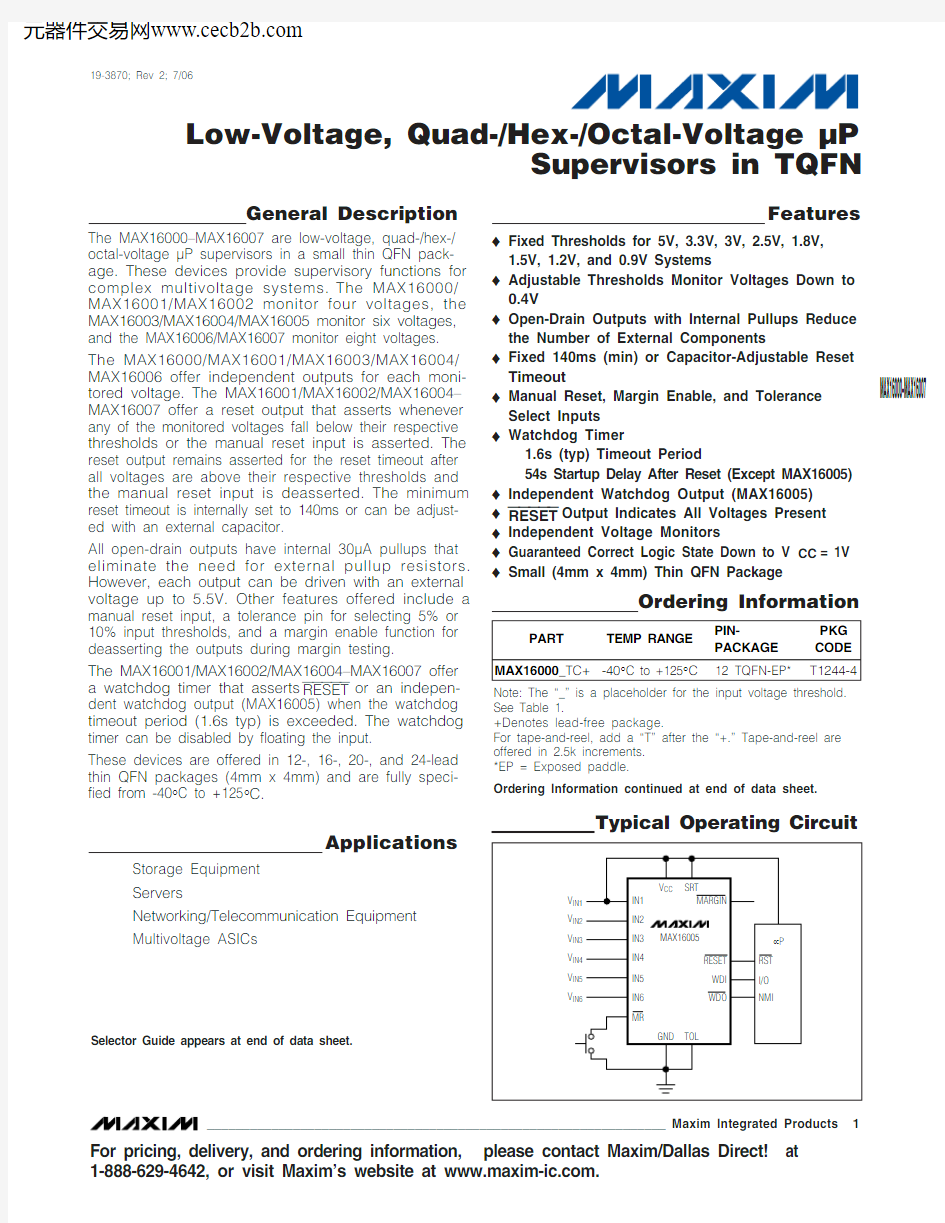
The MAX16000–MAX16007 are low-voltage, quad-/hex-/octal-voltage μP supervisors in a small thin QFN pack-age. These devices provide supervisory functions for complex multivoltage systems.The MAX16000/MAX16001/MAX16002 monitor four voltages, the MAX16003/MAX16004/MAX16005 monitor six voltages,and the MAX16006/MAX16007 monitor eight voltages.The MAX16000/MAX16001/MAX16003/MAX16004/MAX16006 offer independent outputs for each moni-tored voltage. The MAX16001/MAX16002/MAX16004–MAX16007 offer a reset output that asserts whenever any of the monitored voltages fall below their respective thresholds or the manual reset input is asserted. The reset output remains asserted for the reset timeout after all voltages are above their respective thresholds and the manual reset input is deasserted. The minimum reset timeout is internally set to 140ms or can be adjust-ed with an external capacitor.
All open-drain outputs have internal 30μA pullups that eliminate the need for external pullup resistors.However, each output can be driven with an external voltage up to 5.5V. Other features offered include a manual reset input, a tolerance pin for selecting 5% or 10% input thresholds, and a margin enable function for deasserting the outputs during margin testing.
The MAX16001/MAX16002/MAX16004–MAX16007 offer a watchdog timer that asserts RESET or an indepen-dent watchdog output (MAX16005) when the watchdog timeout period (1.6s typ) is exceeded. The watchdog timer can be disabled by floating the input.
These devices are offered in 12-, 16-, 20-, and 24-lead thin QFN packages (4mm x 4mm) and are fully speci-fied from -40°C to +125°C.
Applications
Storage Equipment Servers
Networking/Telecommunication Equipment Multivoltage ASICs
Features
?Fixed Thresholds for 5V, 3.3V, 3V, 2.5V, 1.8V,1.5V, 1.2V, and 0.9V Systems
?Adjustable Thresholds Monitor Voltages Down to 0.4V
?Open-Drain Outputs with Internal Pullups Reduce the Number of External Components
?Fixed 140ms (min) or Capacitor-Adjustable Reset Timeout
?Manual Reset, Margin Enable, and Tolerance Select Inputs ?Watchdog Timer
1.6s (typ) Timeout Period
54s Startup Delay After Reset (Except MAX16005)?Independent Watchdog Output (MAX16005)?RESET Output Indicates All Voltages Present ?Independent Voltage Monitors
?Guaranteed Correct Logic State Down to V CC = 1V ?Small (4mm x 4mm) Thin QFN Package
MAX16000–MAX16007
Low-Voltage, Quad-/Hex-/Octal-Voltage μP
Supervisors in TQFN
________________________________________________________________Maxim Integrated Products 1
Ordering Information
Typical Operating Circuit
19-3870; Rev 2; 7/06
For pricing, delivery, and ordering information,please contact Maxim/Dallas Direct!at 1-888-629-4642, or visit Maxim’s website at https://www.doczj.com/doc/a68831123.html,.
Note: The “_” is a placeholder for the input voltage threshold.See Table 1.
+Denotes lead-free package.
For tape-and-reel, add a “T” after the “+.” Tape-and-reel are offered in 2.5k increments. *EP = Exposed paddle.
Ordering Information continued at end of data sheet.
Selector Guide appears at end of data sheet.
M A X 16000–M A X 16007
Low-Voltage, Quad-/Hex-/Octal-Voltage μP Supervisors in TQFN 2_______________________________________________________________________________________
ABSOLUTE MAXIMUM RATINGS
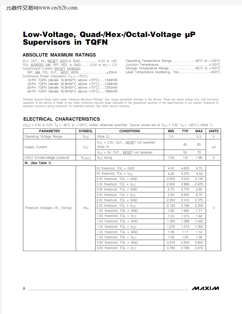
ELECTRICAL CHARACTERISTICS
(V CC = 2.0V to 5.5V, T A = -40°C to +125°C, unless otherwise specified. Typical values are at V CC = 3.3V, T A = +25°C.) (Note 1)
Stresses beyond those listed under “Absolute Maximum Ratings” may cause permanent damage to the device. These are stress ratings only, and functional operation of the device at these or any other conditions beyond those indicated in the operational sections of the specifications is not implied. Exposure to absolute maximum rating conditions for extended periods may affect device reliability.
V CC , OUT_, IN_, RESET , WDO to GND....................-0.3V to +6V TOL, MARGIN , MR , SRT, WDI, to GND..........-0.3V to V CC + 0.3Input/Output Current (RESET , MARGIN ,
SRT, MR , TOL, OUT_, WDO , WDI)..............................±20mA Continuous Power Dissipation (T A = +70°C)
12-Pin TQFN (derate 16.9mW/°C above +70°C)......1349mW 16-Pin TQFN (derate 16.9mW/°C above +70°C)......1349mW 20-Pin TQFN (derate 16.9mW/°C above +70°C)......1355mW 24-Pin TQFN (derate 16.9mW/°C above +70°C)......1666mW
Operating Temperature Range .........................-40°C to +125°C Junction Temperature .....................................................+150°C Storage Temperature Range.............................-65°C to +150°C Lead Temperature (soldering, 10s).................................+300°C
MAX16000–MAX16007
Low-Voltage, Quad-/Hex-/Octal-Voltage μP
Supervisors in TQFN
_______________________________________________________________________________________3
ELECTRICAL CHARACTERISTICS (continued)
M A X 16000–M A X 16007
Low-Voltage, Quad-/Hex-/Octal-Voltage μP Supervisors in TQFN 4_______________________________________________________________________________________
ELECTRICAL CHARACTERISTICS (continued)
Note 2:The outputs are guaranteed to be in the correct logic state down to V CC = 1V.Note 3:Measured with WDI, MARGIN , and MR unconnected.
Note 4:The minimum and maximum specifications for this parameter are guaranteed by using the worst case of the SRT ramp cur-rent and SRT threshold specifications.
Note 5:Guaranteed by design and not production tested.
Note 6:Amount of time required for logic to lock/unlock outputs from margin testing.
Typical Operating Characteristics
(V CC = 3.3V, T A = +25°C, unless otherwise noted.)
SUPPLY CURRENT vs. SUPPLY VOLTAGE
SUPPLY VOLTAGE (V)
S U P P L Y C U R R E N T (μA )
1.5
2.0
2.5
3.0 3.5
4.0 4.5
5.0
5.5
30354045505560
SUPPLY CURRENT vs. TEMPERATURE
TEMPERATURE (°C)
S U P P L Y C U R R E N T (μA )
-40-25-105203550658095110125
30
3540
45505560
NORMALIZED THRESHOLD 2.5vs. SUPPLY VOLTAGE
SUPPLY VOLTAGE (V)
N O R M A L I Z E D T H R E S H O L D
M A X 16000 t o c 03
1.5
2.0
3.0 3.5
4.0 4.5
5.0 5.5
0.990
0.9930.9950.9981.0001.0031.0051.0081.010NORMALIZED THRESHOLD vs. TEMPERATURE
TEMPERATURE (°C)
N O R M A L I Z E D T H R E S H O L D
M A X 16000 t o c 04
-40-25-105203550658095110125
0.995
0.996
0.997
0.9980.9991.0001.001OUTPUT VOLTAGE vs. SINK CURRENT
SINK CURRENT (mA)
V O U T _ (m V )
1
2
34567
8
025
50
75100
OUTPUT VOLTAGE vs. SOURCE CURRENT
SOURCE CURRENT (μA)
V C C - V O U T _ (m V )
5
10152025
30
0200
400
600
8001000
RESET TIMEOUT PERIOD vs. TEMPERATURE
TEMPERATURE (°C)
T I M E O U T P E R I O D (m s )
M A X 16000 t o c 08
-40-25-105203550658095110125
190
191192193194195196197198
1
10
100
1000
MAXIMUM TRANSIENT DURATION
vs. INPUT OVERDRIVE
INPUT OVERDRIVE (mV)
M A X I M U M T R A N S I E N T D U R A T I O N (μs )
6000100200300400500RESET TIMEOUT DELAY
OUT12V/div IN15V/div
40ms/div
RESET 2V/div
MAX16000–MAX16007
Low-Voltage, Quad-/Hex-/Octal-Voltage μP
Supervisors in TQFN
_______________________________________________________________________________________5
Typical Operating Characteristics (continued)
(V CC = 3.3V, T A = +25°C, unless otherwise noted.)
10000.01
0.1
1
10
100
1000
100
10
1
0.10.01
RESET TIMEOUT PERIOD
vs. C SRT
M A X 16000 t o c 10
C SRT (nF)
t R P (m s )
WATCHDOG TIMEOUT PERIOD
vs. TEMPERATURE
TEMPERATURE (°C)
W A T C H D O G T I M E O U T P E R I O D (s )M A X 16000 t o c 11
-40-25-105203550658095110125
1.50
1.51
1.521.531.541.551.561.571.581.591.60
MARGIN ENABLE FUNCTION
MAX16000 toc12
OUT_2V/div
MARGIN 2V/div
100μs/div
RESET 2V/div
OUT_ AND RESET ARE BELOW RESPECTIVE THRESHOLDS MARGIN DISABLE FUNCTION
MAX16000 toc13
OUT_2V/div MARGIN 2V/div
100μs/div
RESET 2V/div
OUT_ AND RESET ARE BELOW RESPECTIVE THRESHOLDS
REFERENCE VOLTAGE vs. SOURCE CURRENT
SOURCE CURRENT (μA)
V R E F (V )
100
200300400500600
1.220
1.2251.2301.2351.2401.245
1.2501.2551.260
REFERENCE VOLTAGE vs. SUPPLY VOLTAGE
SUPPLY VOLTAGE (V)
R E F E R E N C E V O L T A G E (V )
1.5
2.0
2.5
3.0 3.5
4.0 4.5
5.0
5.5
1.220
1.2251.2301.2351.2401.2451.2501.2551.260REFERENCE VOLTAGE vs. TEMPERATURE
TEMPERATURE (°C)
R E F E R E N C E V O L T A G E (V )
-40-25-105203550658095110125
1.20
1.211.221.231.241.251.261.271.28M A X 16000–M A X 16007
Low-Voltage, Quad-/Hex-/Octal-Voltage μP Supervisors in TQFN 6_______________________________________________________________________________________
MAX16000–MAX16007
Low-Voltage, Quad-/Hex-/Octal-Voltage μP
Supervisors in TQFN
_______________________________________________________________________________________7
Pin Description (MAX16000/MAX16001/MAX16002)
M A X 16000–M A X 16007
Low-Voltage, Quad-/Hex-/Octal-Voltage μP Supervisors in TQFN 8_______________________________________________________________________________________
Pin Description (MAX16003/MAX16004/MAX16005)
MAX16000–MAX16007
Low-Voltage, Quad-/Hex-/Octal-Voltage μP
Supervisors in TQFN
_______________________________________________________________________________________9
Pin Description (MAX16003/MAX16004/MAX16005) (continued)
M A X 16000–M A X 16007
Low-Voltage, Quad-/Hex-/Octal-Voltage μP Supervisors in TQFN 10______________________________________________________________________________________
Pin Description (MAX16006/MAX16007)
MAX16000–MAX16007
Low-Voltage, Quad-/Hex-/Octal-Voltage μP
Supervisors in TQFN
______________________________________________________________________________________11
Pin Description (MAX16006/MAX16007) (continued)
M A X 16000–M A X 16007
Low-Voltage, Quad-/Hex-/Octal-Voltage μP Supervisors in TQFN 12______________________________________________________________________________________
MAX16000–MAX16007
Low-Voltage, Quad-/Hex-/Octal-Voltage μP
Supervisors in TQFN
______________________________________________________________________________________13
Figure 1. MAX16000D Functional Diagram
Functional Diagrams
M A X 16000–M A X 16007
Low-Voltage, Quad-/Hex-/Octal-Voltage μP Supervisors in TQFN 14______________________________________________________________________________________
Functional Diagrams (continued)
MAX16000–MAX16007
Low-Voltage, Quad-/Hex-/Octal-Voltage μP
Supervisors in TQFN
______________________________________________________________________________________
15
Figure 3. MAX16003C/MAX16004C Functional Diagram
Functional Diagrams (continued)
M A X 16000–M A X 16007
Low-Voltage, Quad-/Hex-/Octal-Voltage μP Supervisors in TQFN 16______________________________________________________________________________________
Figure 4. MAX16005C Functional Diagram
Functional Diagrams (continued)
MAX16000–MAX16007
Low-Voltage, Quad-/Hex-/Octal-Voltage μP
Supervisors in TQFN
______________________________________________________________________________________17
Figure 5. MAX16006C/MAX16007C Functional Diagram
Functional Diagrams (continued)
M A X 16000–M A X 16007
Low-Voltage, Quad-/Hex-/Octal-Voltage μP Supervisors in TQFN 18______________________________________________________________________________________
Detailed Description
The MAX16000–MAX16007 are low-voltage, quad-/hex-/octal-voltage μP supervisors in a small thin QFN pack-age. These devices provide supervisory functions for complex multivoltage systems. The MAX16000/MAX16001/MAX16002 monitor four voltages, the MAX16003/MAX16004/MAX16005 monitor six voltages,and the MAX16006/MAX16007 monitor eight voltages.The MAX16000/MAX16001/MAX16003/MAX16004/MAX16006 offer independent outputs for each moni-tored voltage. The MAX16001/MAX16002/MAX16004–MAX16007 offer a reset output that asserts whenever any of the monitored voltages fall below their respective thresholds or the manual reset input is asserted. The reset output remains asserted for the reset timeout after all voltages are above their respective thresholds and the manual reset input is deasserted. The minimum reset timeout is internally set to 140ms or can be adjusted with an external capacitor.
All open-drain outputs have internal 30μA pullups that eliminate the need for external pullup resistors.However, each output can be driven with an external voltage up to 5.5V. Other features offered include a manual reset input, a tolerance pin for selecting 5% or 10% input thresholds, and a margin enable function for deasserting the outputs during margin testing.
The MAX16001/MAX16002/MAX16004–MAX16007 offer a watchdog timer that asserts RESET or an indepen-dent watchdog output (MAX16005) when the watchdog timeout period (1.6s typ) is exceeded. The watchdog timer can be disabled by floating the input.
Applications Information
Undervoltage-Detection Circuit
The open-drain outputs of the MAX16000–MAX16007can be configured to detect an undervoltage condition.Figure 6 shows a configuration where an LED turns on when the comparator output is low, indicating an undervoltage condition. These devices can also be used in applications such as system supervisory moni-toring, multivoltage level detection, and V CC bar-graph monitoring (Figure 7).
Tolerance (TOL)
The MAX16000–MAX16007 feature a pin-selectable threshold tolerance. Connect TOL to GND to select 5%threshold tolerance. Connect TOL to V CC to select 10%threshold tolerance.
Window Detection
A window detector circuit uses two auxiliary inputs in the configuration shown in Figure 8. External resistors set the two threshold voltages of the window detector circuit. External logic gates create the OUT signal. The window detection width is the difference between the threshold voltages (Figure 9).
Figure 6. Quad Undervoltage Detector with LED Indicators
Figure 7. V CC Bar-Graph Monitoring
MAX16000–MAX16007
Low-Voltage, Quad-/Hex-/Octal-Voltage μP
Supervisors in TQFN
______________________________________________________________________________________19
Adjustable Input
These devices offer several monitor options with adjustable input thresholds (see Table 1). The threshold voltage at each adjustable IN_ input is typically 0.394V (TOL = GND) or 0.372 (TOL = V CC ). To monitor a voltage V INTH , connect a resistive-divider network to the circuit as shown in Figure 10.
V INTH = V TH ((R1 / R2) + 1)R1 = R2 ((V INTH / V TH ) - 1)
Large resistors can be used to minimize current through the external resistors. For greater accuracy, use lower-value resistors.
Unused Inputs
Connect any unused IN_ inputs to a voltage above its threshold.
OUT_Outputs
(MAX16000/MAX16001/MAX16003/
MAX16004/MAX16006)
The OUT_ outputs go low when their respective IN_inputs drop below their specified thresholds. The output is open drain with a 30μA internal pullup to V CC . For many applications, no external pullup resistor is required
to interface with other logic devices. An external pullup resistor to any voltage from 0 to 5.5V overrides the inter-nal pullup if interfacing to different logic supply voltages.Internal circuitry prevents reverse current flow from the external pullup voltage to V CC (Figure 11).
Figure 10. Setting the Adjustable Input
Figure 9. Output Response of Window Detector Circuit
M A X 16000–M A X 16007
Low-Voltage, Quad-/Hex-/Octal-Voltage μP Supervisors in TQFN 20______________________________________________________________________________________
RESET Output (MAX16001/MAX16002/
MAX16004–MAX16007)
RESET asserts low when any of the monitored voltages fall below their respective thresholds or MR is asserted.RESET remains asserted for the reset timeout period after all monitored voltages exceed their respective thresholds and MR is deasserted (see Figure 12). This open-drain output has a 30μA internal pullup. An exter-nal pullup resistor to any voltage from 0 to 5.5V overrides the internal pullup if interfacing to different logic supply voltages. Internal circuitry prevents reverse current flow from the external pullup voltage to V CC (Figure 11).
WDO (MAX16005 Only)
WDO asserts low whenever the watchdog timer times out or any of the IN_ inputs falls below its respective threshold. WDO deasserts after a valid WDI transition without a reset timeout period. WDO deasserts without
a timeout delay when all the IN_ inputs rise above their thresholds. Pull MR low to deassert WDO . WDO remains deasserted while MR is low. The watchdog timer begins counting after the reset timeout period after MR goes high. Pull MARGIN to deassert WDO .
Reset Timeout Capacitor
The reset timeout period can be adjusted to accommo-date a variety of μP applications from 50μs to 1.12s.Adjust the reset timeout period (t RP ) by connecting a capacitor (C SRT ) between SRT and GND. Calculate the reset timeout capacitor as follows:
Connect SRT to V CC for a factory-programmed reset timeout of 140ms (min).
Figure 11. Interfacing to a Different Logic Supply Voltage Figure 12. Output Timing Diagram