? 2011 Microchip Technology Inc.
DS21143C-page 1
HCS301
FEATURES
Security
?Programmable 28-bit serial number ?Programmable 64-bit encryption key ?Each transmission is unique ?66-bit transmission code length ?32-bit hopping code
?
34-bit fixed code (28-bit serial number, 4-bit button code, 2-bit status)
?Encryption keys are read protected
Operating
? 3.5V - 13.0V operation ?Four button inputs
?No additional circuitry required ?15 functions available ?Selectable baud rate
?Automatic code word completion
?Battery low signal transmitted to receiver ?Battery low indication on LED ?
Non-volatile synchronization data
Other
?Functionally identical to HCS300?Easy-to-use programming interface ?On-chip EEPROM
?On-chip oscillator and timing components
?Button inputs have internal pull-down resistors ?Current limiting on LED output ?
Low external component cost
Typical Applications
The HCS301 is ideal for Remote Keyless Entry (RKE)applications. These applications include:?Automotive RKE systems ?Automotive alarm systems ?Automotive immobilizers
?Gate and garage door openers ?Identity tokens
?
Burglar alarm systems
DESCRIPTION
The HCS301 from Microchip Technology Inc. is a code hopping encoder designed for secure Remote Keyless Entry (RKE) systems. The HCS301 utilizes the K EE L OQ ? code hopping technology, which incorpo-rates high security, a small package outline and low cost, to make this device a perfect solution for unidirec-tional remote keyless entry systems and access control systems.
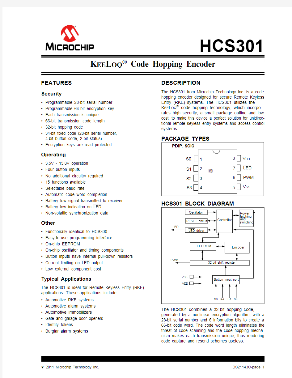
PACKAGE TYPES
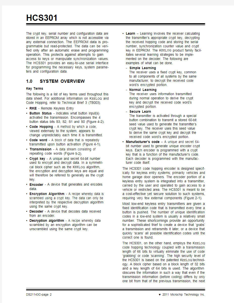
HCS301 BLOCK DIAGRAM
The HCS301 combines a 32-bit hopping code,generated by a nonlinear encryption algorithm, with a 28-bit serial number and 6 information bits to create a 66-bit code word. The code word length eliminates the threat of code scanning and the code hopping mecha-nism makes each transmission unique, thus rendering code capture and resend schemes useless.
1
234
8765
S0S1S2S3
V DD
LED PWM V SS
PDIP , SOIC
HCS301
V SS V DD
Oscillator RESET circuit
LED driver
Controller
Power latching and
switching
Button input port
32-bit shift register
Encoder
EEPROM
PWM
LED
S3S2S1S0
K EE L OQ ? Code Hopping Encoder
HCS301
DS21143C-page 2? 2011 Microchip Technology Inc.
The crypt key, serial number and configuration data are stored in an EEPROM array which is not accessible via any external connection. The EEPROM data is pro-grammable but read-protected. The data can be veri-fied only after an automatic erase and programming operation. This protects against attempts to gain access to keys or manipulate synchronization values.The HCS301 provides an easy-to-use serial interface for programming the necessary keys, system parame-ters and configuration data.
1.0SYSTEM OVERVIEW
Key Terms
The following is a list of key terms used throughout this data sheet. For additional information on K EE L OQ and Code Hopping, refer to Technical Brief 3 (TB003).?RKE - Remote Keyless Entry
?Button Status - Indicates what button input(s) activated the transmission. Encompasses the 4 button status bits S3, S2, S1 and S0 (Figure 4-2).?Code Hopping - A method by which a code, viewed externally to the system, appears to change unpredictably each time it is transmitted.?Code word - A block of data that is repeatedly transmitted upon button activation (Figure 4-1).?Transmission - A data stream consisting of repeating code words (Figure 9-2).
?Crypt key - A unique and secret 64-bit number used to encrypt and decrypt data. In a symmetri-cal block cipher such as the K EE L OQ algorithm, the encryption and decryption keys are equal and will therefore be referred to generally as the crypt key.
?Encoder - A device that generates and encodes data.
?Encryption Algorithm - A recipe whereby data is scrambled using a crypt key. The data can only be interpreted by the respective decryption algorithm using the same crypt key.
?Decoder - A device that decodes data received from an encoder.
?Decryption algorithm - A recipe whereby data scrambled by an encryption algorithm can be unscrambled using the same crypt key.
?Learn – Learning involves the receiver calculating the transmitter’s appropriate crypt key, decrypting the received hopping code and storing the serial number, synchronization counter value and crypt key in EEPROM. The K EE L OQ product family facil-itates several learning strategies to be imple-mented on the decoder. The following are examples of what can be done. -Simple Learning
The receiver uses a fixed crypt key, common to all components of all systems by the same manufacturer, to decrypt the received code word’s encrypted portion.-Normal Learning
The receiver uses information transmitted during normal operation to derive the crypt key and decrypt the received code word’s encrypted portion.-Secure Learn
The transmitter is activated through a special button combination to transmit a stored 60-bit seed value used to generate the transmitter’s crypt key. The receiver uses this seed value to derive the same crypt key and decrypt the received code word’s encrypted portion.
?Manufacturer’s code – A unique and secret 64-bit number used to generate unique encoder crypt keys. Each encoder is programmed with a crypt key that is a function of the manufacturer’s code. Each decoder is programmed with the manufac-turer code itself.The HCS301 code hopping encoder is designed specif-ically for keyless entry systems; primarily vehicles and home garage door openers. The encoder portion of a keyless entry system is integrated into a transmitter,carried by the user and operated to gain access to a vehicle or restricted area. The HCS301 is meant to be a cost-effective yet secure solution to such systems,requiring very few external components (Figure 2-1).Most low-end keyless entry transmitters are given a fixed identification code that is transmitted every time a button is pushed. The number of unique identification codes in a low-end system is usually a relatively small number. These shortcomings provide an opportunity for a sophisticated thief to create a device that ‘grabs’a transmission and retransmits it later, or a device that quickly ‘scans’ all possible identification codes until the correct one is found.
The HCS301, on the other hand, employs the K EE L OQ code hopping technology coupled with a transmission length of 66 bits to virtually eliminate the use of code ‘grabbing’ or code ‘scanning’. The high security level of the HCS301 is based on the patented K EE L OQ technol-ogy. A block cipher based on a block length of 32 bits and a key length of 64 bits is used. The algorithm obscures the information in such a way that even if the transmission information (before coding) differs by only one bit from that of the previous transmission, the next
HCS301
coded transmission will be completely different. Statis-tically, if only one bit in the 32-bit string of information changes, greater than 50percent of the coded trans-mission bits will change.
As indicated in the block diagram on page one, the HCS301 has a small EEPROM array which must be loaded with several parameters before use; most often programmed by the manufacturer at the time of produc-tion. The most important of these are:
? A 28-bit serial number, typically unique for every encoder
? A crypt key
?An initial 16-bit synchronization value
? A 16-bit configuration value The crypt key generation typically inputs the transmitter serial number and 64-bit manufacturer’s code into the key generation algorithm (Figure1-1). The manufac-turer’s code is chosen by the system manufacturer and must be carefully controlled as it is a pivotal part of the overall system security.
FIGURE 1-1:CREATION AND STORAGE OF CRYPT KEY DURING PRODUCTION
The 16-bit synchronization counter is the basis behind the transmitted code word changing for each transmis-sion; it increments each time a button is pressed. Due to the code hopping algorithm’s complexity, each incre-ment of the synchronization value results in greater than 50% of the bits changing in the transmitted code word.
Figure1-2 shows how the key values in EEPROM are used in the encoder. Once the encoder detects a button press, it reads the button inputs and updates the syn-chronization counter. The synchronization counter and crypt key are input to the encryption algorithm and the output is 32 bits of encrypted information. This data will change with every button press, its value appearing externally to ‘randomly hop around’, hence it is referred to as the hopping portion of the code word. The 32-bit hopping code is combined with the button information and serial number to form the code word transmitted to the receiver. The code word format is explained in greater detail in Section4.0.
A receiver may use any type of controller as a decoder, but it is typically a microcontroller with compatible firm-ware that allows the decoder to operate in conjunction with an HCS301 based transmitter. Section7.0 provides detail on integrating the HCS301 into a sys-tem.A transmitter must first be ‘learned’ by the receiver before its use is allowed in the system. Learning includes calculating the transmitter’s appropriate crypt key, decrypting the received hopping code and storing the serial number, synchronization counter value and crypt key in EEPROM.
In normal operation, each received message of valid format is evaluated. The serial number is used to deter-mine if it is from a learned transmitter. If from a learned transmitter, the message is decrypted and the synchro-nization counter is verified. Finally, the button status is checked to see what operation is requested. Figure1-3 shows the relationship between some of the values stored by the receiver and the values received from the transmitter.
Transmitter
Manufacturer’s
Serial Number Code Crypt Key
Key Generation Algorithm
Serial Number
Crypt Key
Sync Counter
.
.
.
HCS301
Production
Programmer
EEPROM Array
? 2011 Microchip Technology Inc.DS21143C-page 3
HCS301
DS21143C-page 4? 2011 Microchip Technology Inc.
FIGURE 1-2:
BUILDING THE TRANSMITTED CODE WORD (ENCODER)
FIGURE 1-3:BASIC OPERATION OF RECEIVER (DECODER)
NOTE: Circled numbers indicate the order of execution.
Button Press Information
EEPROM Array 32 Bits Encrypted Data
Serial Number
Transmitted Information
Crypt Key Sync Counter Serial Number
K EE L OQ ?Encryption Algorithm
Button Press Information
EEPROM Array
Manufacturer Code
32 Bits of Encrypted Data
Serial Number
Received Information
Decrypted Synchronization Counter
Check for Match
Sync Counter Serial Number K EE L OQ ?Decryption Algorithm
134 Check for Match
2 Perform Function Indicated by button press
5
Crypt Key
? 2011 Microchip Technology Inc.DS21143C-page 5
HCS301
2.0
DEVICE OPERATION
As shown in the typical application circuits (Figure 2-1),the HCS301 is a simple device to use. It requires only the addition of buttons and RF circuitry for use as the transmitter in your security application. A description of each pin is given in Table 2-1.FIGURE 2-1:
TYPICAL CIRCUITS
TABLE 2-1:
PIN DESCRIPTIONS
The HCS301 will wake-up upon detecting a button press and delay approximately 10 ms for button debounce (Figure 2-2). The synchronization counter,discrimination value and button information will be encrypted to form the hopping code. The hopping code portion will change every transmission, even if the same button is pushed again. A code word that has been transmitted will not repeat for more than 64K transmissions. This provides more than 18years of use before a code is repeated; based on 10 operations per day. Overflow information sent from the encoder can be used to extend the number of unique transmissions to more than 192K.
If in the transmit process it is detected that a new but-ton(s) has been pressed, a RESET will immediately occur and the current code word will not be completed.Please note that buttons removed will not have any effect on the code word unless no buttons remain pressed; in which case the code word will be completed and the power-down will occur.
Note:
When V DD > 9.0V and driving low capaci-tive loads, a resistor with a minimum value of 50Ω should be used in line with V DD .This prevents clamping of PWM at 9.0V in the event of PWM overshoot.
B0Tx out
S0S1S2S3
LED V DD PWM V SS
2 button remote control
B1
Tx out
S0S1S2S3
LED V DD PWM V SS
5 button remote control (1)
B4 B3 B2 B1 B0
Note 1:
Up to 15 functions can be implemented by pressing more than one button simultaneously or by using a suitable diode array.
2:
Resistor R is recommended for current limiting.
+12V
R +12V
R (2)
(2)
Name Pin Number
Description
S01Switch input 0S12Switch input 1
S23Switch input 2 / Clock pin when in Programming mode S34Switch input 3V SS 5Ground reference
PWM
6
Pulse Width Modulation (PWM)output pin / Data pin for Programming mode LED 7Cathode connection for LED V DD
8
Positive supply voltage
HCS301
DS21143C-page 6? 2011 Microchip Technology Inc.
FIGURE 2-2:
ENCODER OPERATION
3.0
EEPROM MEMORY ORGANIZATION
The HCS301 contains 192 bits (12 x 16-bit words) of EEPROM memory (Table 3-1). This EEPROM array is used to store the encryption key information,synchronization value, etc. Further descriptions of the memory array is given in the following sections.
TABLE 3-1:
EEPROM MEMORY MAP
3.1KEY_0 - KEY_3 (64-Bit Crypt Key)
The 64-bit crypt key is used to create the encrypted message transmitted to the receiver. This key is calcu-lated and programmed during production using a key generation algorithm. The key generation algorithm may be different from the K EE L OQ algorithm. Inputs to the key generation algorithm are typically the transmit-ter’s serial number and the 64-bit manufacturer’s code.While the key generation algorithm supplied from Microchip is the typical method used, a user may elect to create their own method of key generation. This may be done providing that the decoder is programmed with the same means of creating the key for decryption purposes.
Power-Up
RESET and Debounce Delay
(10 ms)
Sample Inputs Update Sync Info Encrypt With Load Transmit Register
Buttons Added ?
All Buttons Released
?(A button has been pressed)
Transmit
Stop
No
Yes
No Yes
Crypt Key Complete Code Word Transmission
WORD ADDRESS
MNEMONIC
DESCRIPTION
0KEY_0 64-bit encryption key
(word 0) LSb’s 1KEY_164-bit encryption key (word 1)
2KEY_2
64-bit encryption key (word 2)
3KEY_3 64-bit encryption key
(word 3) MSb’s 4SYNC
16-bit synchronization value
5RESERVED Set to 0000H 6SER_0
Device Serial Number (word 0) LSb’s
7SER_1(Note)Device Serial Number
(word 1) MSb’s 8SEED_0Seed Value (word 0)9SEED_1Seed Value (word 1)10RESERVED Set to 0000H
11CONFIG
Config Word
Note:
The MSB of the serial number contains a bit used to select the Auto-shutoff timer.
HCS301
3.2SYNC (Synchronization Counter) This is the 16-bit synchronization value that is used to create the hopping code for transmission. This value will increment after every transmission.
3.3 Reserved
Must be initialized to 0000H.
3.4SER_0, SER_1
(Encoder Serial Number)
SER_0 and SER_1 are the lower and upper words of the device serial number, respectively. Although there are 32 bits allocated for the serial number, only the lower order 28 bits are transmitted. The serial number is meant to be unique for every transmitter.
3.4.1AUTO-SHUTOFF TIMER ENABLE The Most Significant bit of the serial number (Bit 31) is used to turn the Auto-shutoff timer on or off. This timer prevents the transmitter from draining the battery should a button get stuck in the on position for a long period of time. The time period is approximately 25seconds, after which the device will go to the Time-out mode. When in the Time-out mode, the device will stop transmitting, although since some circuits within the device are still active, the current draw within the Shutoff mode will be higher than Standby mode. If the Most Significant bit in the serial number is a one, then the Auto-shutoff timer is enabled, and a zero in the Most Significant bit will disable the timer. The length of the timer is not selectable.
3.5SEED_0, SEED_1 (Seed Word)
The 2-word (32-bit) seed code will be transmitted when all three buttons are pressed at the same time (see Figure4-2). This allows the system designer to imple-ment the secure learn feature or use this fixed code word as part of a different key generation/tracking pro-cess.3.6CONFIG (Configuration Word)
The Configuration Word is a 16-bit word stored in EEPROM array that is used by the device to store information used during the encryption process, as well as the status of option configurations. The following sections further explain these bits.
TABLE 3-2:CONFIGURATION WORD
3.6.1DISCRIMINATION VALUE
(DISC0 TO DISC9)
The discrimination value aids the post-decryption check on the decoder end. It may be any value, but in a typical system it will be programmed as the 10 Least Significant bits of the serial number. Values other than this must be separately stored by the receiver when a transmitter is learned. The discrimination bits are part of the information that form the encrypted portion of the transmission (Figure4-2). After the receiver has decrypted a transmission, the discrimination bits are checked against the receiver’s stored value to verify that the decryption process was valid. If the discrimina-tion value was programmed as the 10 LSb’s of the serial number then it may merely be compared to the respective bits of the received serial number; saving EEPROM space.
3.6.2OVERFLOW BITS
(OVR0, OVR1)
The overflow bits are used to extend the number of possible synchronization values. The synchronization counter is 16 bits in length, yielding 65,536 values before the cycle repeats. Under typical use of 10operations a day, this will provide nearly 18 years of use before a repeated value will be used. Should the system designer conclude that is not adequate, then the overflow bits can be utilized to extend the number Bit Number Bit Description
0Discrimination Bit 0
1Discrimination Bit 1
2Discrimination Bit 2
3Discrimination Bit 3
4Discrimination Bit 4
5Discrimination Bit 5
6Discrimination Bit 6
7Discrimination Bit 7
8 Discrimination Bit 8
9Discrimination Bit 9
10Overflow Bit 0 (OVR0)
11Overflow Bit 1 (OVR1)
12Low Voltage Trip Point Select
(V LOW SEL)
13Baud rate Select Bit 0 (BSL0)
14Baud rate Select Bit 1 (BSL1)
15Reserved, set to 0
? 2011 Microchip Technology Inc.DS21143C-page 7
HCS301
DS21143C-page 8? 2011 Microchip Technology Inc.
of unique values. This can be done by programming OVR0 and OVR1 to 1s at the time of production. The encoder will automatically clear OVR0 the first time that the synchronization value wraps from 0xFFFF to 0x0000 and clear OVR1 the second time the counter wraps. Once cleared, OVR0 and OVR1 cannot be set again, thereby creating a permanent record of the counter overflow. This prevents fast cycling of 64K counter. If the decoder system is programmed to track the overflow bits, then the effective number of unique synchronization values can be extended to 196,608.
3.6.3
BAUD RATE SELECT BITS (BSL0, BSL1)
BSL0 and BSL1 select the speed of transmission and the code word blanking. Table 3-3 shows how the bits are used to select the different baud rates and Section 5.7 provides detailed explanation in code word blanking.
TABLE 3-3:
BAUD RATE SELECT
3.6.4
LOW VOLTAGE TRIP POINT SELECT
The low voltage trip point select bit is used to tell the HCS301 what V DD level is being used. This information will be used by the device to determine when to send the voltage low signal to the receiver. When this bit is set to a one, the V DD level is assumed to be operating from a 9V or 12V V DD level. If the bit is set low, then the V DD level is assumed to be 6.0 volts. Refer to Figure 3-1 for volt-age trip point.
FIGURE 3-1:
VOLTAGE TRIP POINTS BY CHARACTERIZATION
BSL1BSL0Basic Pulse Element Code Words Transmitted 00400 μs All 01200 μs 1 out of 210100 μs 1 out of 21
1
100 μs
1 out of 4
-4020
40
100
8.57.58.07.0
9.02.5
3.03.5
4.0
V LOW
Temp (C)
Volts (V)
V LOW sel = 1
V LOW sel = 0
4.5-20
60
805.05.5Max
Min
Max
Min
? 2011 Microchip Technology Inc.DS21143C-page 9
HCS301
4.0
TRANSMITTED WORD
4.1
Code Word Format
The HCS301 code word is made up of several parts (Figure 4-1). Each code word contains a 50% duty cycle preamble, a header, 32 bits of encrypted data and 34 bits of fixed data followed by a guard period before another code word can begin. Refer to Table 9-4 for code word timing.
4.2Code Word Organization
The HCS301 transmits a 66-bit code word when a button is pressed. The 66-bit word is constructed from a Fixed Code portion and an Encrypted Code portion (Figure 4-2).
The 32 bits of Encrypted Data are generated from 4button bits, 12 discrimination bits and the 16-bit sync value. The encrypted portion alone provides up to four billion changing code combinations.
The 34 bits of Fixed Code Data are made up of 2 sta-tus bits, 4 button bits and the 28-bit serial number. The fixed and encrypted sections combined increase the number of code combinations to 7.38x 10¹⁹.
FIGURE 4-1:CODE WORD FORMAT
FIGURE 4-2:CODE WORD ORGANIZATION
LOGIC ‘0’LOGIC ‘1’
Bit Period
Preamble
Header Encrypted Portion of Transmission
Fixed Portion of Transmission Guard
Time T P
T H
T HOP
T FIX
T G
T E
T E T E 50% Duty Cycle
Repeat (1 bit)V LOW (1 bit)Button Status S2 S1 S0 S3
Serial Number (28 bits)
Button Status S2 S1 S0 S3
OVR (2 bits)DISC (10 bits)Sync Counter (16 bits)
Repeat (1 bit)V LOW (1 bit)
Button Status 1 1 1 1
Serial Number (28 bits)
SEED (32 bits)
34 bits of Fixed Portion
32 bits of Encrypted Portion
66 Data bits Transmitted LSb first.
LSb
MSb
MSb
LSb
Note: SEED replaces Encrypted Portion when all button inputs are activated at the same time.
HCS301
DS21143C-page 10? 2011 Microchip Technology Inc.
4.3
Synchronous Transmission Mode
Synchronous Transmission mode can be used to clock the code word out using an external clock.
To enter Synchronous Transmission mode, the Pro-gramming mode start-up sequence must be executed as shown in Figure 4-3. If either S1 or S0 is set on the falling edge of S2 (or S3), the device enters Synchro-nous Transmission mode. In this mode, it functions as a normal transmitter, with the exception that the timing of the PWM data string is controlled externally and 16extra bits are transmitted at the end with the code word.
The button code will be the S0, S1 value at the falling edge of S2 or S3. The timing of the PWM data string is controlled by supplying a clock on S2 or S3 and should not exceed 20 kHz. The code word is the same as in PWM mode with 16 reserved bits at the end of the word. The reserved bits can be ignored. When in Syn-chronous Transmission mode S2 or S3 should not be toggled until all internal processing has been com-pleted as shown in Figure 4-4.
FIGURE 4-3:SYNCHRONOUS TRANSMISSION MODE
FIGURE 4-4:
CODE WORD ORGANIZATION (SYNCHRONOUS TRANSMISSION MODE)
“01,10,11”
PWM
S2
S[1:0]T PS T PH 1T PH 2
t = 50ms
Preamble
Header
Data
Reserved (16 bits)Padding (2 bits)
Button Status S2 S1 S0 S3
Serial Number (28 bits)
Button Status S2 S1 S0 S3
DISC+ OVR (12 bits)Sync Counter (16 bits)
82 Data bits Transmitted LSb first.
LSb
MSb
Fixed Portion
Encrypted Portion
HCS301
5.0SPECIAL FEATURES
5.1Code Word Completion
The code word completion feature ensures that entire code words are transmitted, even if the button is released before the code word is complete. If the but-ton is held down beyond the time for one code word, multiple code words will result. If another button is acti-vated during a transmission, the active transmission will be aborted and a new transmission will begin using the new button information.
5.2 LED Output Operation
During normal transmission the LED output is LOW. If the supply voltage drops below the low voltage trip point, the LED output will be toggled at approximately 5Hz during the transmission (Section3.6.4).
5.3RPT: Repeat Indicator
This bit will be low for the first transmitted word. If a button is held down for more than one transmitted code word, this bit will be set to indicate a repeated code word and remain set until the button is released.
5.4V LOW: Voltage LOW Indicator
The V LOW signal is transmitted so the receiver can give an indication to the user that the transmitter battery is low. The V LOW bit is included in every transmission (Figure4-2 and Figure9-5) and will be transmitted as a zero if the operating voltage is above the low voltage trip point. Refer to Figure4-2. The trip point is select-able based on the battery voltage being used. See Sec-tion 3.6.3 for a description of how the low voltage trip point is configured.
5.5Auto-shutoff
The Auto-shutoff function automatically stops the device from transmitting if a button inadvertently gets pressed for a long period of time. This will prevent the device from draining the battery if a button gets pressed while the transmitter is in a pocket or purse. This function can be enabled or disabled and is selected by setting or clearing the Auto-shutoff bit (see Section3.4.1). Setting this bit high will enable the func-tion (turn Auto-shutoff function on) and setting the bit low will disable the function. Time-out period is approx-imately 25 seconds.5.6Seed Transmission
In order to increase the level of security in a system, it is possible for the receiver to implement what is known as a secure learn function. This can be done by utilizing the seed value stored in EEPROM, transmitted only when all three button inputs are pressed at the same time (Table5-1). Instead of the normal key generation inputs being used to create the crypt key, this seed value is used.
TABLE 5-1:PIN ACTIVATION TABLE
Function S3S2S1S0 Standby00000
Hopping Code
10001
20010
-----
131101
141110 Seed Code151111
? 2011 Microchip Technology Inc.DS21143C-page 11
HCS301
DS21143C-page 12? 2011 Microchip Technology Inc.
5.7
Blank Alternate Code Word
Federal Communications Commission (FCC) part 15rules specify the limits on worst case average funda-mental power and harmonics that can be transmitted in a 100ms window. For FCC approval purposes, it may therefore be advantageous to minimize the transmis-sion duty cycle. This can be achieved by minimizing the duty cycle of the individual bits as well as by blanking out consecutive code words. Blank Alternate Code Word (BACW) may be used to reduce the average power of a transmission by transmitting only every sec-ond code word (Figure 5-1). This is a selectable feature that is determined in conjunction with the baud rate selection bit BSL0.
Enabling the BACW option may likewise allow the user to transmit a higher amplitude transmission as the time averaged power is reduced. BACW effectively halves the RF on time for a given transmission so the RF out-put power could theoretically be doubled while main-taining the same time averaged output power.
FIGURE 5-1:BLANK ALTERNATE CODE WORD (BACW)
Code Word BACW Disabled (All words transmitted)BACW Enabled (1 out of 2 transmitted)
BACW Enabled (1 out of 4 transmitted)
A 2A
4A
Amplitude
Time
Code Word Code Word Code Word
? 2011 Microchip Technology Inc.DS21143C-page 13
HCS301
6.0
PROGRAMMING THE HCS301
When using the HCS301 in a system, the user will have to program some parameters into the device including the serial number and the secret key before it can be used. The programming cycle allows the user to input all 192 bits in a serial data stream, which are then stored internally in EEPROM. Programming will be initiated by forcing the PWM line high, after the S2 (or S3) line has been held high for the appropriate length of time line (Table 6-1 and Figure 6-1). After the Pro-gram mode is entered, a delay must be provided to the device for the automatic bulk write cycle to complete.This will set all locations in the EEPROM to zeros. The device can then be programmed by clocking in 16 bits at a time, using S2 (or S3) as the clock line and PWM as the data in line. After each 16-bit word is loaded, a
programming delay is required for the internal program cycle to complete. This delay can take up to T WC . At the end of the programming cycle, the device can be veri-fied (Figure 6-2) by reading back the EEPROM. Read-ing is done by clocking the S2 (or S3) line and reading the data bits on PWM. For security reasons, it is not possible to execute a verify function without first pro-gramming the EEPROM. A Verify operation can only be done once, immediately following the Program cycle . FIGURE 6-1:PROGRAMMING WAVEFORMS
FIGURE 6-2:VERIFY WAVEFORMS
Note:
To ensure that the device does not acci-dentally enter Programming mode, PWM should never be pulled high by the circuit connected to it. Special care should be taken when driving PNP RF transistors.
PWM Enter Program
Mode
(Data)
(Clock)
Note 1: Unused button inputs to be held to ground during the entire programming sequence.
Bit 0
Bit 1
Bit 2
Bit 3
Bit 14
Bit 15
Bit 16
Bit 17
T PH 1
T PBW
T PS Repeat for each word (12 times)
T PH 2
T CLKH
T CLKL
T WC
T DS
S2 (S3) Data for Word 0 (KEY_0)
Data for Word 1
T DH
2: The V DD pin must be taken to ground after a Program/Verify cycle.
PWM (Clock)
(Data)Note: If a Verify operation is to be done, then it must immediately follow the Program cycle.
End of Programming Cycle Beginning of Verify Cycle
Bit 1Bit 2Bit 3 Bit 15Bit 14Bit 16Bit 17Bit190Bit191
T WC Data from Word 0
T DV
S2 (S3)Bit 0Bit191Bit190
HCS301
TABLE 6-1:PROGRAMMING/VERIFY TIMING REQUIREMENTS
V DD = 5.0V ± 10%, 25 °C ± 5 °C
Parameter Symbol Min.Max.Units Program mode setup time T PS 3.5 4.5ms
Hold time 1T PH1 3.5—ms
Hold time 2T PH250—μs
Bulk Write time T PBW 4.0—ms Program delay time T PROG 4.0—ms Program cycle time T WC50—ms
Clock low time T CLKL50—μs
Clock high time T CLKH50—μs
Data setup time T DS0—μs(1)
Data hold time T DH30—μs(1)
Data out valid time T DV—30μs(1)
Note1:Typical values - not tested in production.
DS21143C-page 14? 2011 Microchip Technology Inc.
HCS301
7.0INTEGRATING THE HCS301
INTO A SYSTEM
Use of the HCS301 in a system requires a compatible decoder. This decoder is typically a microcontroller with compatible firmware. Microchip will provide (via a license agreement) firmware routines that accept transmissions from the HCS301 and decrypt the hopping code portion of the data stream. These routines provide system designers the means to develop their own decoding system.
7.1Learning a Transmitter to a
Receiver
A transmitter must first be 'learned' by a decoder before its use is allowed in the system. Several learning strat-egies are possible, Figure7-1 details a typical learn sequence. Core to each, the decoder must minimally store each learned transmitter's serial number and cur-rent synchronization counter value in EEPROM. Addi-tionally, the decoder typically stores each transmitter's unique crypt key. The maximum number of learned transmitters will therefore be relative to the available EEPROM.
A transmitter's serial number is transmitted in the clear but the synchronization counter only exists in the code word's encrypted portion. The decoder obtains the counter value by decrypting using the same key used to encrypt the information. The K EE L OQ algorithm is a symmetrical block cipher so the encryption and decryp-tion keys are identical and referred to generally as the crypt key. The encoder receives its crypt key during manufacturing. The decoder is programmed with the ability to generate a crypt key as well as all but one required input to the key generation routine; typically the transmitter's serial number.
Figure7-1 summarizes a typical learn sequence. The decoder receives and authenticates a first transmis-sion; first button press. Authentication involves gener-ating the appropriate crypt key, decrypting, validating the correct key usage via the discrimination bits and buffering the counter value. A second transmission is received and authenticated. A final check verifies the counter values were sequential; consecutive button presses. If the learn sequence is successfully com-plete, the decoder stores the learned transmitter's serial number, current synchronization counter value and appropriate crypt key. From now on the crypt key will be retrieved from EEPROM during normal opera-tion instead of recalculating it for each transmission received.
Certain learning strategies have been patented and care must be taken not to infringe.FIGURE 7-1:TYPICAL LEARN
SEQUENCE
Enter Learn
Mode
Wait for Reception
of a Valid Code
Generate Key
from Serial Number
Use Generated Key
to Decrypt
Compare Discrimination
Value with Fixed Value
Equal
Wait for Reception
of Second Valid Code
Compare Discrimination
Value with Fixed Value
Use Generated Key
to Decrypt
Equal
Counters
Encryption key
Serial number
Synchronization counter
Sequential
?
?
?
Exit
Learn successful Store:
Learn
Unsuccessful
No
No
No
Yes
Yes
Yes
? 2011 Microchip Technology Inc.DS21143C-page 15
HCS301
DS21143C-page 16? 2011 Microchip Technology Inc.
7.2
Decoder Operation
Figure 7-2 summarizes normal decoder operation. The decoder waits until a transmission is received. The received serial number is compared to the EEPROM table of learned transmitters to first determine if this transmitter's use is allowed in the system. If from a learned transmitter, the transmission is decrypted using the stored crypt key and authenticated via the discrimination bits for appropriate crypt key usage. If the decryption was valid the synchronization value is evaluated.
FIGURE 7-2:
TYPICAL DECODER OPERATION
7.3
Synchronization with Decoder (Evaluating the Counter)
The K EE L OQ technology patent scope includes a sophisticated synchronization technique that does not require the calculation and storage of future codes. The technique securely blocks invalid transmissions while providing transparent resynchronization to transmitters inadvertently activated away from the receiver. Figure 7-3 shows a 3-partition, rotating synchronization window. The size of each window is optional but the technique is fundamental. Each time a transmission is authenticated, the intended function is executed and the transmission's synchronization counter value is stored in EEPROM. From the currently stored counter value there is an initial "Single Operation" forward win-dow of 16 codes. If the difference between a received synchronization counter and the last stored counter is within 16, the intended function will be executed on the single button press and the new synchronization coun-ter will be stored. Storing the new synchronization counter value effectively rotates the entire synchroniza-tion window.
A "Double Operation" (resynchronization) window fur-ther exists from the Single Operation window up to 32K codes forward of the currently stored counter value. It is referred to as "Double Operation" because a trans-mission with synchronization counter value in this win-dow will require an additional, sequential counter transmission prior to executing the intended function.Upon receiving the sequential transmission the decoder executes the intended function and stores the synchronization counter value. This resynchronization occurs transparently to the user as it is human nature to press the button a second time if the first was unsuc-cessful.
The third window is a "Blocked Window" ranging from the double operation window to the currently stored synchronization counter value. Any transmission with synchronization counter value within this window will be ignored. This window excludes previously used,perhaps code-grabbed transmissions from accessing the system.?
Transmission Received
Does
Serial Number
Match ?
Decrypt Transmission
Is Decryption Valid ?
Is Counter Within 16
?
Is Counter Within 32K
?Update Counter
Execute Command Save Counter in Temp Location
Start
No
No
No
No
Yes
Yes
Yes
Yes
Yes
No
and No
Note:
The synchronization method described in this section is only a typical implementation and because it is usually implemented in firmware, it can be altered to fit the needs of a particular system.
? 2011 Microchip Technology Inc.DS21143C-page 17
HCS301
FIGURE 7-3:
SYNCHRONIZATION WINDOW
Blocked Entire Window rotates to eliminate use of previously used codes
Single Operation
Window Window (32K Codes)
(16 Codes)
Double Operation (resynchronization)
Window (32K Codes)
Stored
Synchronization Counter Value
HCS301
DS21143C-page 18? 2011 Microchip Technology Inc.
8.0
DEVELOPMENT SUPPORT
The PIC ? microcontrollers and dsPIC ? digital signal controllers are supported with a full range of software and hardware development tools:
?Integrated Development Environment -MPLAB ? IDE Software
?Compilers/Assemblers/Linkers
-MPLAB C Compiler for Various Device Families
-HI-TECH C for Various Device Families -MPASM TM Assembler -MPLINK TM Object Linker/MPLIB TM Object Librarian
-MPLAB Assembler/Linker/Librarian for Various Device Families ?Simulators
-MPLAB SIM Software Simulator ?Emulators
-MPLAB REAL ICE? In-Circuit Emulator ?In-Circuit Debuggers -MPLAB ICD 3
-PICkit? 3 Debug Express ?Device Programmers -PICkit? 2 Programmer
-MPLAB PM3 Device Programmer
?Low-Cost Demonstration/Development Boards, Evaluation Kits, and Starter Kits
8.1
MPLAB Integrated Development Environment Software
The MPLAB IDE software brings an ease of software development previously unseen in the 8/16/32-bit microcontroller market. The MPLAB IDE is a Windows ?operating system-based application that contains:? A single graphical interface to all debugging tools -Simulator
-Programmer (sold separately)
-In-Circuit Emulator (sold separately)-In-Circuit Debugger (sold separately)
? A full-featured editor with color-coded context ? A multiple project manager
?Customizable data windows with direct edit of contents
?High-level source code debugging ?Mouse over variable inspection
?Drag and drop variables from source to watch windows
?Extensive on-line help
?Integration of select third party tools, such as IAR C Compilers The MPLAB IDE allows you to:
?Edit your source files (either C or assembly)
?One-touch compile or assemble, and download to emulator and simulator tools (automatically updates all project information)?Debug using:
-Source files (C or assembly)-Mixed C and assembly -Machine code MPLAB IDE supports multiple debugging tools in a single development paradigm, from the cost-effective simulators, through low-cost in-circuit debuggers, to full-featured emulators. This eliminates the learning curve when upgrading to tools with increased flexibility and power.
HCS301
8.2MPLAB C Compilers for Various
Device Families
The MPLAB C Compiler code development systems are complete ANSI C compilers for Microchip’s PIC18, PIC24 and PIC32 families of microcontrollers and the dsPIC30 and dsPIC33 families of digital signal control-lers. These compilers provide powerful integration capabilities, superior code optimization and ease of use.
For easy source level debugging, the compilers provide symbol information that is optimized to the MPLAB IDE debugger.
8.3HI-TECH C for Various Device
Families
The HI-TECH C Compiler code development systems are complete ANSI C compilers for Microchip’s PIC family of microcontrollers and the dsPIC family of digital signal controllers. These compilers provide powerful integration capabilities, omniscient code generation and ease of use.
For easy source level debugging, the compilers provide symbol information that is optimized to the MPLAB IDE debugger.
The compilers include a macro assembler, linker, pre-processor, and one-step driver, and can run on multiple platforms.
8.4MPASM Assembler
The MPASM Assembler is a full-featured, universal macro assembler for PIC10/12/16/18 MCUs.
The MPASM Assembler generates relocatable object files for the MPLINK Object Linker, Intel? standard HEX files, MAP files to detail memory usage and symbol reference, absolute LST files that contain source lines and generated machine code and COFF files for debugging.
The MPASM Assembler features include:?Integration into MPLAB IDE projects
?User-defined macros to streamline
assembly code
?Conditional assembly for multi-purpose
source files
?Directives that allow complete control over the assembly process 8.5MPLINK Object Linker/
MPLIB Object Librarian
The MPLINK Object Linker combines relocatable objects created by the MPASM Assembler and the MPLAB C18 C Compiler. It can link relocatable objects from precompiled libraries, using directives from a linker script.
The MPLIB Object Librarian manages the creation and modification of library files of precompiled code. When a routine from a library is called from a source file, only the modules that contain that routine will be linked in with the application. This allows large libraries to be used efficiently in many different applications.
The object linker/library features include:
?Efficient linking of single libraries instead of many smaller files
?Enhanced code maintainability by grouping related modules together
?Flexible creation of libraries with easy module listing, replacement, deletion and extraction
8.6MPLAB Assembler, Linker and
Librarian for Various Device
Families
MPLAB Assembler produces relocatable machine code from symbolic assembly language for PIC24, PIC32 and dsPIC devices. MPLAB C Compiler uses the assembler to produce its object file. The assembler generates relocatable object files that can then be archived or linked with other relocatable object files and archives to create an executable file. Notable features of the assembler include:
?Support for the entire device instruction set ?Support for fixed-point and floating-point data ?Command line interface
?Rich directive set
?Flexible macro language
?MPLAB IDE compatibility
? 2011 Microchip Technology Inc.DS21143C-page 19
HCS301
DS21143C-page 20? 2011 Microchip Technology Inc.
8.7
MPLAB SIM Software Simulator
The MPLAB SIM Software Simulator allows code development in a PC-hosted environment by simulat-ing the PIC MCUs and dsPIC ? DSCs on an instruction level. On any given instruction, the data areas can be examined or modified and stimuli can be applied from a comprehensive stimulus controller. Registers can be logged to files for further run-time analysis. The trace buffer and logic analyzer display extend the power of the simulator to record and track program execution,actions on I/O, most peripherals and internal registers. The MPLAB SIM Software Simulator fully supports symbolic debugging using the MPLAB C Compilers,and the MPASM and MPLAB Assemblers. The soft-ware simulator offers the flexibility to develop and debug code outside of the hardware laboratory envi-ronment, making it an excellent, economical software development tool.
8.8
MPLAB REAL ICE In-Circuit Emulator System
MPLAB REAL ICE In-Circuit Emulator System is Microchip’s next generation high-speed emulator for Microchip Flash DSC and MCU devices. It debugs and programs PIC ? Flash MCUs and dsPIC ? Flash DSCs with the easy-to-use, powerful graphical user interface of the MPLAB Integrated Development Environment (IDE),included with each kit.
The emulator is connected to the design engineer’s PC using a high-speed USB 2.0 interface and is connected to the target with either a connector compatible with in-circuit debugger systems (RJ11) or with the new high-speed, noise tolerant, Low-Voltage Differential Signal (LVDS) interconnection (CAT5).
The emulator is field upgradable through future firmware downloads in MPLAB IDE. In upcoming releases of MPLAB IDE, new devices will be supported, and new features will be added. MPLAB REAL ICE offers significant advantages over competitive emulators including low-cost, full-speed emulation, run-time variable watches, trace analysis, complex breakpoints, a ruggedized probe interface and long (up to three meters)interconnection cables.
8.9
MPLAB ICD 3 In-Circuit Debugger System
MPLAB ICD 3 In-Circuit Debugger System is Micro-chip's most cost effective high-speed hardware debugger/programmer for Microchip Flash Digital Sig-nal Controller (DSC) and microcontroller (MCU)devices. It debugs and programs PIC ? Flash microcon-trollers and dsPIC ? DSCs with the powerful, yet easy-to-use graphical user interface of MPLAB Integrated Development Environment (IDE).
The MPLAB ICD 3 In-Circuit Debugger probe is con-nected to the design engineer's PC using a high-speed USB 2.0 interface and is connected to the target with a connector compatible with the MPLAB ICD 2 or MPLAB REAL ICE systems (RJ-11). MPLAB ICD 3 supports all MPLAB ICD 2 headers.
8.10
PICkit 3 In-Circuit Debugger/Programmer and
PICkit 3 Debug Express
The MPLAB PICkit 3 allows debugging and program-ming of PIC ? and dsPIC ? Flash microcontrollers at a most affordable price point using the powerful graphical user interface of the MPLAB Integrated Development Environment (IDE). The MPLAB PICkit 3 is connected to the design engineer's PC using a full speed USB interface and can be connected to the target via an Microchip debug (RJ-11) connector (compatible with MPLAB ICD 3 and MPLAB REAL ICE). The connector uses two device I/O pins and the reset line to imple-ment in-circuit debugging and In-Circuit Serial Pro-gramming?.
The PICkit 3 Debug Express include the PICkit 3, demo board and microcontroller, hookup cables and CDROM with user’s guide, lessons, tutorial, compiler and MPLAB IDE software.
毕业论文论文题目(中文)JPEG图像的编解码实现 论文题目(外文)Encoding and decoding of JPEG image
摘要 JPEG是一种十分先进的图像压缩技术,它用有损压缩方式去除冗余的图像数据,在获得极高的压缩率的同时能展现十分丰富生动的图像。本文设计和实现一个JPEG图像编解码器来进行图像转换,利用离散余弦变换、熵编码、Huffman编码等图像压缩技术将BMP图像转换成JPEG图像,即进行图像的压缩。验证JPEG压缩编码算法的可行性。通过比对图像压缩前后实际效果,探讨压缩比,峰值信噪比等评价图像数据压缩程度及压缩质量的关键参数,对JPEG 压缩编码算法的实用性和优越性进行研究。 关键词:JPEG;编码;解码;图像压缩
Abstract JPEG is a very advanced image compression technology, it uses lossy compression to remove redundant image data, in obtaining a very high compression rate can show a very rich and vivid image. In this project, a JPEG image codec is designed and implemented to transform image, using discrete cosine transform, entropy coding, Huffman coding and other image compression techniques to convert BMP images into JPEG images. Verifies the feasibility of JPEG compression coding algorithm. Through the comparison of the actual effect of image compression, the key parameters of compression ratio, peak Snr, and the compression quality of image data are discussed, and the practicability and superiority of JPEG compression coding algorithm are researched. Key words: JPEG; encoding; decoding; image compression
高清解码器快速使用说明书 目录 第一章产品介绍 (2) 1.1产品概述 (2) 1.2产品主要功能特点 (2) 第二章设备线缆连接 (3) 第三章基本操作 (4) 3.1开机 (4) 3.2关机 (4) 3.3登录 (4) 3.4预览 (5) 3.5报警功能 (5) 3.5.1移动侦测 (5) 3.6网络设置 (6) 3.7通道管理 (6) 3.8公网访问设备(云操作) (7) 3.8.1向导 (7) 3.8.2按用户登录,管理设备(按用户登录,可以管理多台设备) (10) 3.8.3按序列号登录,访问设备 (12) 第四章远程监控 (13) 1.远程监控 (13) 1.1多机管理平台软件CMS (13) 1.2web监控 (13) 2.基本远程操控 (15) 2.1画面分割 (15) 2.2回放 (15) 2.3日志 (15) 2.4本地配置 (15) 2.5通道操控 (15) 2.6远程进行设备端配置 (15)
第一章产品介绍 1.1产品概述 本设备是专为安防领域设计的一款优秀的数字监控产品。采用嵌入式LINUX操作系统,使系统运行更稳定;采用标准的H.264MP视频压缩算法和独有的时空滤波算法,实现了高画质、低码率的同步音视频监控;采用TCP/IP等网络技术,具有强大的网络数据传输能力和远程操控能力。 本设备既可本地独立工作,也可连网组成一个强大的安全监控网,配合专业网络视频监控平台软件,充分体现出其强大的组网和远程监控能力。 1.2产品主要功能特点 本产品是由4块BLK3520A_N04A_H组合成的一款4路高清解码器,通过网络将数据接收进来,支持4路1080P解码,视频输出支持4路TV,4路VGA,4路HDMI同时输出。4块BLK3520A_N04A_H独立使用,共用1个电源和1个网口。
图像编码技术的研究和应用 一幅二维图像可以表示为将一个二维亮度函数通过采样和量化而得到的一个二维数组。这样一个二维数组的数据量通常很大,从而对存储、处理和传输都带来了许多问题,提出了许多新的要求。为此人们试图采用对图像新的表达方法以减少表示一幅图像需要的数据量,这就是图像编码所要解决的主要问题。压缩数据量的主要方法是消除冗余数据,从数学角度来讲是要将原始图像转化为从统计角度看尽可能不相关的数据集。这个转换要在图像进行存储、处理和传输之前进行,而在这之后需要将压缩了的图像解压缩以重建原始图像或其近似图像.图像压缩和图像解压缩,通常也分别称为图像编码和图像解码。 图像编码系统模型模型主要包括2个通过信道级连接的结构模块 :编码器和解码器。当一幅输入图像送入编码器后 ,编码器根据输入数据进行信源编码产生一组信号。这组信号在进一步被信道编码器编码后进入信道。通过信道传输后的码被送入信道解码器和信源解码器 ,解码器重建输出的图像。一般来说 ,输出图是输入图的精确复制 ,那么系统是无失真的或者信息保持型的 ;否则 ,称系统是信息损失的。 现代编码方法 这里介绍了几种比较热的编码方法:第二代编码方法、分形编码、模型编码、神经网络编码、小波变换编码。 1.第二代图像编码方法 第二代图像编码方法是针对传统编码方法中没有考虑人眼对轮廓、边缘的特殊敏感性和方向感知特性而提出的。它认为传统的第一代编码技术以信息论和数字信号处理技术为理论基础 ,出发点是消除图像数据的统计冗余信息 ,包括信息熵冗余、空间冗余和时间冗余。其编码压缩图像数据的能力已接近极限 ,压缩比难提高。第二代图像编码方法充分利用人眼视觉系统的生理和心理视觉冗余特性以及信源的各种性质以期获得高压缩比,这类方法一般要对图像进行预处理,将图像数据根据视觉敏感性进行分割。 2.分形图像编码 分形图像编码是在分形几何理论的基础上发展起来的一种编码方法。分形理论是欧氏几何相关理论的扩展,是研究不规则图形和混沌运动的一门新科学。它描述了自然界物体的自相似性,这种自相似性可以是确定的,也可以是统计意义上的。这一理论基础决定了它只有对具备明显自相似性或统计自相似性的图像,例如海岸线,云彩,大树等才有较高的编码效率。而一般图像不具有这一特性,因此编码效率与图像性质学特性有关 ,而且分形图像编码方法实质上是通过消除图像的几何冗余度来压缩数据的 ,根本没有考虑人眼视觉特性的作用。 3.基于模型的图像编码 基于模型的图像编码技术是近几年发展起来的一种很有前途的编码方法。它利用了计算机视觉和计算机图形学中的方法和理论 ,其基本出发点是在编、解码两端分别建立起相同的模型 ,针对输入的图像提取模型参数或根据模型参数重建图像。模型编码方法的核心是建模和提取模型参数,其中模型的选取、描述和建立是决定模型编码质量的关键因素。为了对图像数据建模, 一般要求对输入图像要有某些先验知识。目前研究最多、进展最快的是针对可视电话应用中的图像序列编码。这类应用中的图像大多为人的头肩像。 4.神经网络图像编码
利用Plug-in(NPAPI)技术扩展应用程序的Web应用 摘要:讨论Plug-in的基本原理和开发方法,实现了一个H.263解码器的插件,并研究了如何把应用程序通过Plug-in技术嵌入浏览器中。 关键词:浏览器Netscape/Mozilla Plug-in 插件MIME Plug-in是扩展浏览器功能的一项重要技术。通过Plug-in技术,各种应用程序和集成软件能够以插件模型直接嵌入到网页中,提供灵活的Web应用。但是对于一些大型的独立应用程序很难将其改造成插件模型。本文主要介绍如何利用Plug-in技术把一个大型或单独运行的应用程序嵌入到浏览器中。 1 Plug-in的开发结构 1.1 Plug-in的基本原理 Plug-in是Netscape公司提出的一种浏览器插件技术。Plug-in插件的生存周期完全由网页控制。具体控制过程如下。 (1)当浏览器读取HTML网页时,若遇到MIME类型的标记时,它首先搜索是否有注册该类型的Plug-in插件。 (2)如果有,将该Plug-in插件的代码载入内存。 (3)浏览器初始化Plug-in的环境。 (4)创建该Plug-in插件的实例,用于处理和显示网页中指定的数据流。 (5)当该网页关闭或转到后台时,浏览器销毁该Plug-in插件的实例。 (6)浏览器关闭前,退出Plug-in的环境。 由如上过程可以看出,Plug-in在运行时完全作为浏览器的一部分。但是,由于Plug-in的编写一般由第三方创建,所以Plug-in插件的开发必须遵循Netscape公司提出的标准规范。Plug-in技术的应用非常广泛,一般浏览器中的多媒体显示都是通过插件的方式由第三方提供的, 如Flash等。 1.2 Plug-in的基本结构 Plug-in虽然是一个独立的模块,但它是由Mozilla浏览器来调用的。本质上说,Plug-in接管了一个指定大小的显示窗口,窗口的绘制和内容显示则完全由Plug-in插件来控制。所以开发者可以将所提供的任何功能和应用放置在该窗口中。
第一章数字视频概述 1.什么是复合视频?2页,可改为填空题 例如:黑白视频信号是一个已经经过加工处理并包含扫描同步和消隐的图像信号,通常也叫做复合视频,简称视频。由于频带范围在1-6MHZ人们又把它叫做电视基带视频。 2.什么是视频技术?它主要应用在哪些领域?3页,可以改为填空题 例如:在不考虑电视调制发射和接收等诸多环节时,单纯考虑和研究电视基带信号的摄取、改善、传输、记录、编辑、显示的技术就叫做视频技术。 主要应用领域:广播电视的摄录编系统、安全及监控、视频通信和视频会议、远程教育及视听教学、影像医学、影音娱乐和电子广告。 3.什么是数字视频?5页 广义的数字视频表述为数字视频是指依据人的视觉暂留特性,借着计算机或微处理器芯片的高速运算,加上Codec技术、传输存储技术等来实现的以比特流为特征的,能按照某种时基规律和标准在显示终端上再现活动影音的信息媒介。狭义的数字视频时指与具体媒体格式所对应的数字视频。 第二章彩色数字视频基础 1.彩色电视系统是根据色光三基色原理来再现彩色图像的。按照此原理,任何一种色光颜色都可以用R G B三个彩色分量按一定的比例混合得到。7页 2.匹配兼容制彩色电视亮度信号的公式是:8页(2-2) 3.两个色差信号正交调制的目的是什么?10页 4.电视扫描分为逐行扫描和隔行扫描两种。 5.电视基带视频有复合视频、亮色分离视频和分量视频三种。13页 6.彩色电视制式有哪三种?制式差异主要体现在哪些方面?14页或改为填空 世界上现行的彩色电视制式有NTSC制式、PAL制式和SECAM制式三大制式。制式差异主要体现在亮度合成公式、色差信号提取、色副载选取及其正交调制类型、扫描方式、同步时基确定等方面的参数。 7.彩色电视图像的数字化有信号上游数字化和信号下游数字化两种。 8.A/D转换主要包括哪些环节?量化的实质是什么?编码的实质是什么?17,18页,可改为填空 A/D转换就是指对幅值连续变化的模拟视频电信号进行脉冲抽样保持、量化、编码等环节后形成二进制码流的技术处理过程。 9.一般常用的线性D/A转换器,其输出模拟电压U和输入数字量D之间成正比关系。19页 10.YCbCr信号和YUV信号是正比关系。21页,或选择A正比B反比C非线性D平方11.CCIR601标准为NTSC、PAL、和SECAM制式规定了共同的图像采样频率是13.5MHZ。21页 12.PAL制NTSC制的现行标准数字电视有效显示分辨率(清晰度)各为720X576像素和720X480像素。公用中分辨率为352X288像素。23页 第三章广义数字视频及分类 1.广义数字视频的定义?28页 2.广义的数字视频是依据人的视觉暂留特性,借助计算机或微处理器芯片的高速运算加上Codec编解码技术、传输存储技术等来实现的比特流为特征的全新的信息媒介。 3.图像序列的特点有哪些?33页 特点是每帧的分辨率相同,图像内容相关、图像文件名连续编号,而且有表示开始的图像序列头和表示结束的图像终止码。
EasyDecoder视频解码管理软件 用户使用说明
目录 目录 (2) 1.系统说明 (5) 1.1概要 (5) 1.2功能简介与特点 (5) 1.3硬件配置 (5) 1.4软件平台与运行环境 (5) 1.5术语 (5) 1.6阅读指导 (6) 2.系统安装 (6) 2.1安装软件 (6) 3.系统主界面 (7) 4.系统运行操作 (7) 4.1进入系统/退出系统 (7) 进入系统 (8) 退出系统 (8) 4.2系统初始化 (8) 4.2.1服务器设置 (9) 4.2.1.1添加服务器 (9) 4.2.1.2智能添加服务器 (10) 4.2.1.3删除服务器 (11) 4.2.1.4修改服务器 (12) 4.2.1.5批量修改服务器 (14) 4.2.1.6反选功能 (14) 4.2.1.7检索服务器 (14) 4.2.1.8修改通道信息 (15) 4.2.2监控点管理 (15)
4.2.3解码器设置 (16) 4.2.3.1手动添加 (16) 4.2.3.2智能添加 (17) 4.2.3.3删除解码器 (17) 4.2.3.4修改解码器名称 (17) 4.2.3.5连接解码器 (18) 4.2.3.6断开解码器 (18) 4.2.3.7解码器设置 (18) 4.2.3.7.1网络设置 (19) 4.2.3.7.2DNS设置 (19) 4.2.3.7.3解码器参数设置 (20) 4.2.3.7.3.1485设置 (20) 4.2.3.7.3.2协议设置 (21) 4.2.3.7.4LOGO设置 (21) 4.2.3.7.5报警设置 (21) 4.2.4联机切换设置 (22) 4.2.4.1添加切换序列 (22) 4.2.4.2删除切换序列 (23) 4.2.4.3连接监控点 (23) 4.2.4.4停止预览 (24) 4.2.4.5打开/关闭音频 (24) 4.2.4.6开始/关闭对讲 (24) 4.2.4.7设备控制 (25) 4.2.4.8开始/停止切换 (26) 4.2.4.9显示模式设置 (26) 4.2.4.10其他 (26) 4.2.4.10.1切换不在线跳过显示 (26)
图像编解码技术及应用 1.图像编解码技术概论: 在当前的图像压缩领域中常用的技术有: BMP、EPS、GIF、JPG、PDF、PIC、PNG、PSD、TIF。上述技术间的差异主要存在于图像编解码的算法不同,通过对算法的研究可以使我们更加容易的理解图像压缩的原理。 位图格式(BMP)是在DOS时代就出现的一种元老级文件格式,因此它是DOS和WINDOWS操作系统上的标准的WINGDOWS点阵图像格式,以此文件格式存储时,采用一种非破坏性的RLE压缩,不会省略任何图像的细部信息。 EPS是最常见的线条稿共享文件格式,它是以PostScript语言为开发基础,所以EPS文件能够同时兼容矢量和点阵图形,所有的排版或图像处理软件如PageMaker或Illustrator等,都提供了读入或置入EPS格式文件的能力,而且RGB和CMYK对象也可以保有各自的原始的色彩模式。 GIF应该是在网络上最常见的一种压缩文件格式,它的英文全名Graphic Interchange format,当初研发的目的是为了最小化电缆上的传输,因此能采用LZW方式进行压缩,但可显示的颜色范围只局限于256索引色,目前所采用 的GIF图形共有两种格式:87a和89a,常见于网页上建议的小动画制作,其中GIF89a还可提供透明色效果,点阵图形,灰度图形或者索引颜色模式皆可存储为此种文件格式 JPG跟GIF一样为网络上最常见道的图像格式,其英文正式名称为Joint Photographic Experts Group,它是以全彩模式进行显示色彩,是目前最有效率的一种压缩格式,常用于照片或连续色调的显示,而且没有GIF去掉图像细 部信息的缺点,但需要注意的是此类图像需要自行设置压缩程度,在打开时JPG 图像会自动解压缩,不过要注意的是JPG采用的压缩是破坏性的压缩,因此会在一定程度上减损图像本身的品质。
输入(INPUT) 输出(OUTPUT)
列的UI 作为一项临时措施,这种全面的组件清单已采取从Foobar的维基页面牌照根据GNU免费文件。 列界面(foo_ui_columns)很受欢迎foobar2000记录备用接口布局的基础上柱和面板。 列有它自己的UI插件系统,这些插件扩展用户界面: 1. 专辑封面面板(foo_uie_albumart)面板显示专辑封面。 2. 专辑封面面板的Matroska(foo_uie_albumart_mka) Albumart国防部阅读Matroska的封面。 3. 相册列表面板(foo_uie_albumlist)一个TreeView显示数据库中使用可自定义排序方式(按流派,艺术家,目录等) 4. 书签(foo_uie_bookmarks)帮你记住歌曲的位置英寸 5. 控制台(foo_uie_console)面板控制台版本。显示诊断消息。 0.1.3用户界面需要列Beta 1或更新版本。 6. 可停靠的面板(foo_dockable_panels),它允许你创建窗口,每个窗口或其他主机的用户界面主要foobar2000记录列小组为浮动的窗口,可以附着在侧。 7. Explorer面板(foo_uie_explorer)显示所选文件夹树视图磁盘/。 8. 歌词面板(foo_uie_lyrics_panel)显示歌词存储在文件标签。 9. 音乐浏览器(foo_browser)面板浏览图书馆,类似于iTunes。 10. 播放列表下拉(foo_uie_playlists_dropdown)显示在一个下拉菜单列表。 11. 播放列表树(foo_playlist_tree)树的媒体库中有许多可供自定义。 12. ProjectM可视化委员会(foo_uie_vis_projectM)的基础上ProjectM项目,这是一个重新实现的Milkdrop下的OpenGL。 13. 队列管理器(foo_uie_queuemanager),它提供了一个窗口,显示队列的内容,并允许你删除其中某些部分或清除整个队列。 14. 快速搜索小组(foo_uie_quicksearch)搜索工具栏,发送结果到播放列表。 15. 单柱播放列表查看器(foo_uie_single_column_playlist)显示单一的“柱”头的音乐库中。为创造一个有益的窄和小的布局。 16. 标签(foo_uie_tabs)标签允许你打破在同一时间泡利的不相容原理相同位置放置多个面板中。 17. 轨道信息小组(foo_uie_trackinfo)使用TAGZ显示曲目信息有关选定。 18. 轨道信息小组国防部(foo_uie_trackinfo_mod)改进的轨道信息面板面板的能力,同时使用多种字体英寸也有能力来显示图像。 显卡 显卡窗口(foo_ui_gfx)是一个可更换皮肤的用户界面,它不只是集中在寻找良好,但试图尽可能快和“轻量级”的可能,也。它使用的Lua语言作为脚本。两张皮包括在存档。 面板的用户界面 面板用户界面(foo_ui_panels)进行管理的能力提供了多个面板槽titleformating。 标准 默认用户界面(foo_ui_std)。包括在标准安装包。 DSP的 1. 4Front耳机(foo_dsp_headphones9)影响对耳机的用户。 2. ATSurround处理器(foo_dsp_atsurround)再现环绕材料和更健全的信息存在于许多立体声音频。 3. BS2D(foo_dsp_bs2p)提高耳机听定期记录高保真立体声。 4. 语音滤波器(foo_dsp_centercut)语音切滤波器。 5. 通道混合器(foo_channel_mixer)向上/向下混合/从1-6频道。 6. 卷积(foo_convolve)注意到脉冲响应和脉冲响应做了快速的数据与该卷积的声音。 7. 推杆(foo_dsp_crossfader)允许淡入淡出轨道之间。 8. 砂轮上(foo_dsp_crossfeed)过滤器的音乐,以帮助减少疲劳而引起的耳机与听音乐。 9. 杜比耳机包装(foo_dsp_dolbyhp)杜比耳机发动机的DLL。 10. 杜比定向逻辑II包装(foo_dsp_pl2)杜比定向逻辑II引擎的DLL(DLL中不包括)。
终端解码器的设计和应用 祁同林蒋虹 摘要介绍了一种在电视摄像监控系统中广泛使用的设备——终端解码器的工作原理、硬件电路设计和控制软件设计。 关键词电视监控系统解码器驱动电路云台 1 概述 云台和变焦镜头是电视摄像监控系统中常用的设备,与摄像机配合使用,可以大大扩大摄像机的监视范围、监视视野和清晰度。常用的电动云台通常可作上、下、左、右4个方向的运动,其控制电压通常为交流24 V和220 V,也有直流12 V控制的电机。变焦镜头通常有光圈、聚焦、变倍3个电机,控制电压一般为直流6 V~9 V。对于安装在室外的摄像机,还需加装室外防护罩,增加风扇、雨刮、加热功能。 由于摄像机一般远离控制室,如用多芯电缆直接传送这十几个控制电压,既浪费线材,又有许多能量损耗在传输电缆上。目前广泛采用计算机进行控制命令的串行传输,只需一根2芯控制电缆,但必须在摄像机附近配置一个终端解码器,将计算机的控制命令进行解码,并转换为相应的控制电压。 2 终端解码器硬件电路设计 终端解码器电路以单片机为核心,包括电平转换、单片机处理器、光电隔离、镜头驱动电路、云台驱动电路、防护罩控制电路、电源控制电路、云台位置控制电路、自动复位电路等,如图1所示。 图 1 解码器电路方框图 远距离传送的控制信号一般均采用RS-485电平,因此,必须把RS-485电平转换成TTL电平。单片机对控制信号解码后,其输出信号端口到驱动电路之间要加光电隔离器件,以防止驱动电路中的继电器、可
控硅等器件对单片机产生干扰。在防护罩控制电路和电源控制电路中,主要是根据输出电流的大小,选用不同功率的继电器来控制防护罩、摄像机电源和照明电源等。 单片机处理电路是解码器的核心部分,一般采用有串行口输入的单片机(如AT89C51),配合一个地址拨码开关,由单片机内部的控制软件对控制信号接收、校验、确认后,将控制命令解码,由I/O口发出相应的控制命令。由于驱动电路中有继电器、可控硅等器件,闭合、断开时容易对单片机产生干扰,同时解码器附近的大型设备的起动、关断也易引起对微机的干扰,容易引起程序进入死循环,不能回到正常工作状态。为了防止软件死机,需要增加自动复位电路。单片机处理电路方框图见图2。 图 2 单片机处理电路方框图 单片机输出的控制信号是TTL电平,为驱动变焦镜头的电机,需要加驱动电路。镜头驱动电路常用的有继电器驱动、运放和晶体管放大驱动等。 云台电机大多采用交流电机,所以其驱动电路除继电器驱动外,目前一般采用双向可控硅驱动电路。双向可控硅的耐压值一般应该取为被控制电压的3~4倍。 3 终端解码器控制软件设计 单片机控制程序流程如图3所示。
H265(HEVC Heigh Efficiency Video Coding)介绍 1 概要 H.265(高效率视频编码(HEVC))是现行“H.264/MPEG-4 AVC”标准于2003年实现标准化以来时隔10年推出的新标准,将成为支撑未来十年的影像服务和产品的视频压缩技术。其特点是,支持1080p以上的4K×2K和8K×4K分辨率,将视频压缩率提高至H.264的约2倍。也就是说,能以原来一半的编码速度发送相同画质的视频。例如,按照20Mbit/秒发送的H.264格式视频内容,在相同画质的条件下用HEVC格式只需10Mbit/秒的速度。 1.1 H.265发展背景 H.264虽然是一个划时代的数字视频压缩标准,但是随着数字视频产业链的高速发展,H.264的局限性逐步显现,并且由于H.264标准核心压缩算法的完全固化,并不能够通过调整或扩充来更好地满足当前高清数字视频应用。 视频应用向以下几个方面发展的趋势愈加明显: (1)高清晰度(Higher Definition):数字视频的应用格式从720P向1080P全面升级,在一些视频应用领域甚至出现了4K*2K、8K*4K的数字视频格式 (2)高帧率(Higher frame rate):数字视频帧率从30fps向60fps、120fps甚至240fps的应用场景升级 (3)高压缩率(Higher Compression rate):传输带宽和存储空间一直是视频应用中最为关键的资源,因此,在有限的空间和管道中获得最佳的视频体验一直是用户的不懈追求。 由于数字视频应用在发展中面临上述趋势,如果继续采用H.264编码就出现如下一些局限性: (1)宏块个数的爆发式增长,会导致用于编码宏块的预测模式、运动矢量、参考帧索引和量化级等宏块级参数信息所占用的码字过多,用于编码残差部分的码字明显减少。即:单个宏块所表示的图像内容的信息大大减少,导致4*4或8*8块变换后的低频率相似程度也大大提高,会出现大量的冗余 (2)分辨率的大幅增加,表示同一个运动的运动矢量的幅值将大大增加,H.264中采用一个运动矢量预测值,对运动矢量差编码使用的是哥伦布指数编码,该编码方式的特点是数值越小使用的比特数越少。因此,随着运动矢量幅值的大幅增加,H.264中用来对运动矢量进行预测以及编码的方法压缩率将逐渐降低。 (3)并行度比较低 H.264的一些关键算法,例如采用CAVLC和CABAC两种基于上下文的熵编码方法、deblock滤波等都要求串行编码,并行度比较低。针对GPU/DSP/FPGA/ASIC等这种并行化程序非常的CPU,H.264的这种串行化处理越来越成为制约运算性能的瓶颈。 基于以上视频应用的发展趋势和H.264的局限性,面向更高清晰度、更高帧率、更高压
H.264可扩展视频编解码器(SVC)应用详解 可扩展视频编解码器已经被开发了许多年。广播行业严格地受到业已建立的各种标准的控制,因此在采用这一技术上一直反应迟缓。处理器、传感器以及显示技术的进步正在点爆各种视频应用。互联网以及IP技术正无缝地把视频伺服至更为不同和远程的由显示设备构成的社群。可扩展视频编解码器——如H.264 SVC 满足了许多这些系统的需求,并且它们可能促使视频被广泛采纳为通信媒介的催化剂。 编解码器被用于压缩视频,以减小传输视频流所需要的带宽,或者,降低把视频文件存档所需要的存储空间。这种压缩的代价就是增大计算要求:压缩比越高,对计算能力的要求就越高。 在带宽与计算要求之间做出折中,对于定义承载编码视频流所需要的最小信道带宽以及编码设备的最小指标均有影响。在传统的像广播电视机这样的视频系统中,解码器的最小规范(在机顶盒的情形下)易于被定义。 然而,目前视频被越来越多地由各种各样的应用所采用,相应地,有各种各样的客户设备,这些设备包括从计算机观看互联网视频,到便携式数字助理(PDA)以及小巧的蜂窝电话。针对这些设备的视频流必需是不同的。 为了更好地兼容特定的观看设备以及信道带宽,必须采用不同的设置对视频流多次编码。每一个设置的组合必须向用户产生一个满足视频流传输所需带宽的视频流以及对观看设备进行解码的能力。如果原始解压视频流不可用,那么,编码视频流必须首先被解码,然后采用新的设置进行解码。这种做法是十分昂贵的。 在理想的情形下,视频仅仅以高效率的编解码器被编码一次。如果经过解码的话,得到的视频流会产生全分辨率的视频。此外,在理想的情形下,如果较低分辨率或带宽的视频流需要被进一步延伸至网络之中,以锁定较低性能的设备,那么,可以不必采取附加的处理,就能够发送一小部分的编码视频。这种较小的视频流便于解码并产生较低分辨率的视频。以这种方式,编码视频流自身就能够适应它需要经过的信道带宽以及目标设备的性能。这些就是可扩展视频编解码器的品质所在。 H.264 可扩展视频编解码器 扩展至H.264的可扩展视频编解码器(H.264 SVC),被设计来传递上述理想情形的各种好处。它以H.264先进视频编解码器标准(H.264 AVC)为基础,并高度利用了原始编解码器的各种工具以及概念。然而,它产生的编码视频是空间上临时可扩展的,并且是在视频质量方面可扩展的。也就是说,它能够产生不同帧速率、分辨率或质量等级的解码视频。 SVC扩展引入了一种原始H.264 AVC编解码器—在编码视频内的各层—不存在的概念。基础层对视频流的最低临时、空间和品质表现进行编码。增强各层利用基
Premiere常用插件下载及说明(转) 小灰熊卡拉ok制作软件 简介:制作卡拉ok字幕的绝佳软件,因其软件本身带有premiere插件,可以作为一个premiere 的外挂使用,更方便了使用者的使用。最重要是,网上有大量的已做好的ksc字幕角本文件,也使得字幕的制作更加的简单化了。 https://www.doczj.com/doc/a25200832.html,/image/boorok.rar最著名的插件-Hollywood FX(好莱坞转场插件) 简介:知名度很高的好莱坞转场插件,FX除了基本的100种效果外,另外还有Plus组188种效果和Pro组96种效果,共计384个这些外加效果的原文件如果是Setup.exe或*.HFZ文件,可以直接安装,如果是解压好分存在Effects、Images和Objects三个目录中的文件,可以直接将这三个目录拷贝到Hollywood FX目录下,覆盖原有目录就可以了。不论是哪种方法添加了新的效果,都要将Hollywood FX目录中Orgs目录内的文件删除,然后再运行Hollywood FX,新的效果才会出现。 https://www.doczj.com/doc/a25200832.html,/image/Hollywood%20FX%20PRO5.1.rar PREMIERE的雨雪插件FE 简介:粒子效果的premiere 的插件,可以模仿雨、雪、气泡等。安装后,PREMIERE可增加下雨、下雪等滤镜。此插件对于PREMIERE5.0的支持比较好,对于6.0和6.5版本,在WIN98下可以进行模版的输出,但不能进行具体的设置调节,在WIN2000下可以进行具体设置调节。 https://www.doczj.com/doc/a25200832.html,/image/finaleff.rar LSX 简介:将A VI转换至MPEG-1或MPEG-2的编码工具。本版本可作为PREMIERE的插件使用,具批处理与VideoCD输出的功能。它是同类插件中速度比较快的,质量中等,适合使用我们模板的用户中比较看重输出速度的用户。 https://www.doczj.com/doc/a25200832.html,/image/lsxmpeg20.rar■PICVIDEO—A VI压缩编码器 简介:A VI文件解码器PICVIDEO,内含最新版本,使用电子相册模板时必须安装的视频压缩编码软件,具有极高的压缩比。配合在PREMIERE下的插件来输出MPG的效果很好。如果不安装它某些A VI文件在播放时上下会出现未解压字符。 https://www.doczj.com/doc/a25200832.html,/image/picvideo210022.rar 百老汇的视频解码程序 简介:百老汇的视频解码程序,有一些视频文件是用百老汇压缩的,必须安装它之后才能进行正常的读取。 https://www.doczj.com/doc/a25200832.html,/image/blh.rar Premiere电子相册模板定位器 简介:只要分三步,模板就可以轻松定位,再也不需要文件一个个查找了。 https://www.doczj.com/doc/a25200832.html,/image/ahdvppj.rar TMPGEnc(小日本) 简介:是premiere直接输出MPEG的最好插件,也是A VI转MPEG的最好插件 这款由日本人堀浩行开发的MPEG编码工具软件,支持VCD、SVCD、DVD等各种格式。它能将各种常见影片文件甚至JPG图片压缩、转换成符合各类光盘格式(如VCD、SVCD、DVD等),成品可直接刻录流通,加上简单易用,使它成为目前最受欢迎的影片压缩软件之一。除了可以压MPEG1/MPEG2外,它还有附加一些MPEG辅助工具,可以对影片进行Multiplex,Demultiplex,Cut/Join等处理、剪接。给影片加片头等特效,字幕组必备。这款软件的优点在于:
在闭路监控系统中,解码器是一个重要的前端控制设备。在主机的控制下,解码器可使云台、镜头、雨刮器和照明灯等前端设备产生相应的动作。 解码器电路板正面示意图 本解码器可用RS232或RS485两种方式进行控制。在距离较近(小于100米)且云台数量不多(少于4个)时,可直接用RS232方式进行控制。在距离较远或云台数量较多时,需用RS485方式进行控制。工程上建议使用RS485方式,其最远控制距离可达1200米,总线最多可驱动64个负载,即64个解码器可并接在同一RS485总线上。
本解码器的RS485总线具有瞬变电压抑制功能,能防雷电和抗静电放电冲击。此外,解码器的所有输出均具有短路保护功能。一旦输出短路,内部电路将自动切断输出电流。此时应断开供电电源,确保排除短路故障,等待30秒后重新上电,解码器即可重新恢复正常工作。此功能对设备具有良好的保护作用。 接线及调试说明: 在完成所有连接之前,请不要接通电源,在确保连接无误后方可通电! (1)~POWER(黄色端子)为解码器电源输入,一般应接入~220V电源。有些 解码器应特殊要求,已改为~24V供电方式,则应接入~24V电源,而禁止接入~220V电源。接入正确电源后,解码器右侧上方的红色电源指示灯亮起。否则应检查电源接插件P1、P2和保险丝(5A)。 (2)RS232、RS485为通信接口,使用时只能连接其中之一。接入RS232时, 要注意正负极性,一般计算机的9针RS232串口输出的3脚为正,5脚为负,开机后这两根控制线不能短路,否则极易损坏计算机的串口;接入RS485时,也应按RS485的极性正确连接。 (3)云台、镜头控制线的接法如示意图所示,左面两排接线端子对应标志接 上即可。云台控制电压由JX1引出的接插件进行选择。当该接插件与P3相接时,可控制~220V云台;与P4相接时,即可控制~24V云台。解码器出厂时,设置为控制~24V云台。 (4)镜头控制电压可由电位器VR1进行无级调节,范围为5V—12V。逆时针方 向旋转电压增高,镜头动作加快;顺时针方向旋转电压降低,镜头动作变慢。VR1的右侧有两个测试点,用万用表可测试其直流电压,出产设置为8V左右。 (5)~OUT输出的交流电用来控制防护罩的雨刮器,其电压由JX2引出的接插 件进行选择。当该接插件与P5相接时,输出电压为~220V;与P6相接时,输出电压为~24V。出厂时,设置~OUT将输出~24V。 (6)~LIGHT输出交流电用来控制照明灯等,电压为~220V,最大电流为5A。 (7)O/C是常开的继电器输出,可用来控制交流或直流的通断,最大电压 250V,最大可通过电流为7A。 (8)AGND和+12V可为摄像机提供直流12V电源,最大电流800mA。 (9)~24V可为摄像机提供交流24V电源,最大电流500mA。 (10)为了调试方便,电路板上还提供了“镜头手动控制”、“云台及其它输出 手动控制”等控制口。调试时,可用短路块短接控制口相应的左右铜柱,查看对应的动作指示灯是否亮起,以及输出电压是否正常。
基于压缩感知的图像视频编解码技术研究 摘要: 随着多媒体和互联网技术的迅速发展,人们对数字图像视频信息(如数码图片、流媒体视频、监控视频)的需求越来越高。而数码相机的广泛应用,又衍生出高分辨率、低功耗、低成本图片和视频的需求。传统的图像视频采集方式,通常是通过获得超过有效维度的高密度观测样本。这种过度采样方式,不仅对硬件设备要求高,要求高密度的传感器;而且为了满足后续存储和传输的需求,采集得到的大量观测样本需要经过复杂的编码过程。压缩感知理论的提出,为新型低复杂度编码器的设计提供了可能性。它指出,如果一个信号在某个变换域下是稀疏的,那么仅需极少量的观测值,就可以通过优化方法高质量地恢复出原始信号。这样,基于压缩感知理论进行图像视频的采集,从而大幅度降低了为了精确重建原始信号所需要的观测值数目,在信号采集阶段就隐含着降低了信号维度,从而大大简化了后续的压缩编码过程。压缩感知理论,改变了图像视频的采集、编码和重建方式,在低功耗编码器(如分布式视频)、低成本采集设备(如高速摄像机)等应用方面具有明显优势。 本文基于压缩感知理论,针对图像和视频的编解码技术进行研究,设计出高效的编码和重建算法;并将其与传统的图像视频编解码方案相结合,在保证标准兼容的基础上,利用压缩感知技术提高编码效率。本文的创新点包括以下四个方面: 1.基于条带差分预测的压缩感知图像编码算法 在图像压缩感知系统的编码端,图像信号的采集方式,以及如何有效地对采集到的观测值进行压缩,是影响整个系统性能的关键性因素。本文提出了一种基于条带差分预测编码的压缩感知图像编码方法。将一幅图像划分为由多行像素点组成的条带,以条带为单位进行采样和编码。与图像块的划分方式相比,具有同样像素点个数的条带更扁平,从而相邻条带之间更为接近,它们的观测值也就具有更高的相关性。实验还表明,在同样的重建算法下,条带划分相比于块划分能够在保证同等重建质量的前提想,产生更小的码率。将这种条带划分方式与差分预测编码框架相结合,设计出一种条带观测值之间的预测机制。由此计算得到的观测值的残差相比原始观测值具有更低的能量,从而达到更高的压缩效率。压缩
单线能实现同步传输曼彻斯特编码 光纤灭”。传输比特速率为2.5Mbit/s或其整数倍。采样率为4KHz和12.8KHz。光波长范围为820nm~860nm(850nm),光缆类型为62.5/125μm多模光纤,光纤接头宜采用ST或FC接头。 数字编码采用曼彻斯特编码,首先传输MSB(最高有效位)。曼彻斯特编码:从高位转移到低位(下降沿)为二进制1,从低位转移到高位(上升沿)为二进制0,即图1的Manchester G.E.Thomas。 图 1 曼切斯特编码传输协议 1、编码 如图1所示,曼切斯特编码一种简单的实现就是数据和时钟的异或,这种实现的前提是数据是依据时钟信号进行输出,即当前的数据和时钟是同步的,这种方式实现在数据和时钟的边沿处可能会出现毛刺信号。如果数据和时钟异步的,那毛刺信号就很多了,就不能简单采用异或的方式实现。因此为了得到质量较好的曼切斯特编码不能简单的采用异或方式实现,另一种实现方式就是采用两倍的是时钟进行调制,即得到时钟双边沿,双边沿采用数据,依据数据的电平决定输出的信号,较好的实现方式就是采用状态机进行转换,由于实现比较复杂因此也就不详细讲解了。 2、解码 如图1所示,曼切斯特解码一种简单的实现就是曼切斯特信号和时钟的异或,这种实现是不稳定的,因为解码端的时钟和编码端时钟是很难保证一样,都有各自的时钟抖动和偏差。因此保证正确的解码,一种好的实现方式是采用高频时钟信号去采用曼切斯特信号,得到曼切斯特信号的脉宽和边沿类型,脉宽可以得到时钟频率,脉宽和边沿一起可以解码出具体数据,由于实现比较复杂因此也就不详细讲解了。 3、应用 由于曼切斯特编码具有自同步能力和良好的抗干扰性能,因此在智能变电站中,互感器采样得到数据传输通信就采用了曼切斯特编码作为传输协议,并定义了数据传输规约,简称为FT3。FT3是IEC60044-8电子式电流互感器标准里规定使用的帧格式,所以描述FT3实际上要从IEC60044-8的标准说起。FT3的数据传输采用串行传输,可采用异步方式传输,也可采用同步方式传输。 FT3同步传输介质宜采用光纤传输系统,逻辑“1”定义为“光纤亮”,逻辑“0”定义为“光纤灭”。传输比特速率为2.5Mbit/s或其整数倍。采样率为4KHz和12.8KHz。光波长范围为820nm~860nm(850nm),光缆类型为 62.5/125μm多模光纤,光纤接头宜采用ST或FC接头。 数字编码采用曼彻斯特编码,首先传输MSB(最高有效位)。曼彻斯特编码:从高位转移到低位(下降沿)为二进制1,从低位转移到高位(上升沿)为二进制0,即图1的Manchester G.E.Thomas。 FT3帧结构如表1所示。 (1) 每帧固定长度,每个字节8位。 (2) 每帧由起始符开始,起始符由两个字节组成,固定为0x0564。 (3) 报文类型:表示不同的帧类型和数据长度、信息排序。 (4) 用户数据,不同帧类型代表的意义不同。 (5) 用户数据之后跟随一个16位的CRC校验序列,由下列多项式生成校验,序列码为 X16+X13+X12+X11+X10+X8+X6+X5+X2+1,生成的16比特校验序列再取反成为所要求的校验序列。
视频编解码技术解析 一、编解码技术的发展现状分析 视频监控技术经过多年的发展,监控画面正经历着从最初的D1标清图像,向4K高清、8K超清时代前进。由于CCD与CMOS技术的发展,前端摄像机的像素越来越高,成本也在逐渐降低,高清监控得到了快速的普及和应用,随之而来的问题是,前端像素的提高给视频传输和后端录像存储带来了巨大的压力,在相同的编码压缩比例下,用户需要投入更多的设备和资金,因此编解码技术的改进无疑成为了视频监控技术发展的焦点,也是当前众多视频厂商争相发展的技术课题。 目前国内主流视频监控设备厂商如大华、海康等,从前端球机、枪机,到后端的 NVR/ESS/EVS存储、矩阵等设备,普遍使用的是MPEG-4与H.264编解码技术,因为MPEG-4/H.264编码技术比较成熟,相应的编解码芯片厂商也较多,因此使用最为广泛,不同厂家设备之间的兼容性也好。但随着500W/800W/1200W等高清摄像机推广应用,网络传输带宽与录像存储空间却承受着严峻的考验,优化算法、提高压缩效率、减少时延的需求使H.265编码技术标准应势而生,它将在未来逐步地被广泛使用。 同时,由于H.264/H.265是ITU-T国际电联组织制定提出的一系列视频编码标准,是一个全世界公开的协议标准,为提高视频数据安全保密性,保障视频信息质量,由我国公安部第一研究所牵头组织,在现有视频编码标准技术的基础上,通过创新的技术改进和加密,形成了一套我国自有的安全防范监控数字视音频编解码技术标准,简称SVAC标准,它在政府类监控项目采购中率先推广应用。 因此来说,在目前的视频监控行业领域,基本保持着MPEG-4/H.264为主,H.265/SVAC 为辅的局面。 二、主要编解码技术的应用现状 在视频监控设备领域,目前主要采用的编解码标准为MPEG-4/H.264技术,当然,随着H.265芯片技术的不断成熟,凭借其更强的优越性能,将会逐步取代H.264并成为行业的主流应用技术。大安防系列化产品也将从前端、存储到解码会发生全面性的变化。下面我们将对目前主要的几种编解码技术的发展和应用做具体介绍。 1. MPEG-4编码技术 MPEG:Moving Pictures Experts Group动态图象专家组,是一个致力于运动图像及其伴音的压缩编码标准化工作的组织,MPEG-4是在MPEG-1、MPEG-2基础上发展而来,