HD74HC139
Dual 2-to-4-line Decoders/Demultiplexers
REJ03D0571-0200
(Previous ADE-205-445)
Rev.2.00
Oct 11, 2005 Description
The HD74HC139 contains two independent two-to-four-line decoders each with a single active low enable input (1G or 2G). Data on the select inputs (1A and 1B or 2A and 2B) cause one of the four normally high outputs to go low. Features
? High Speed Operation: t pd (A, B to Y, 4 levels) = 14 ns typ (C L = 50 pF)
? High Output Current: Fanout of 10 LSTTL Loads
? Wide Operating Voltage: V CC = 2 V to 6 V
? Low Input Current: 1 μA max
? Low Quiescent Supply Current: I CC (static) = 4 μA max (Ta = 25°C)
? Ordering Information
Part Name Package Type
Package Code
(Previous Code)
Package
Abbreviation
Taping Abbreviation
(Quantity)
HD74HC139P DILP-16
pin PRDP0016AE-B
(DP-16FV)
P —
HD74HC139FPEL SOP-16 pin (JEITA) PRSP0016DH-B
(FP-16DAV)
FP EL (2,000 pcs/reel)
HD74HC139TELL TSSOP-16
pin PTSP0016JB-A
(TTP-16DAV)
T ELL (2,000 pcs/reel)
Note: Please consult the sales office for the above package availability.
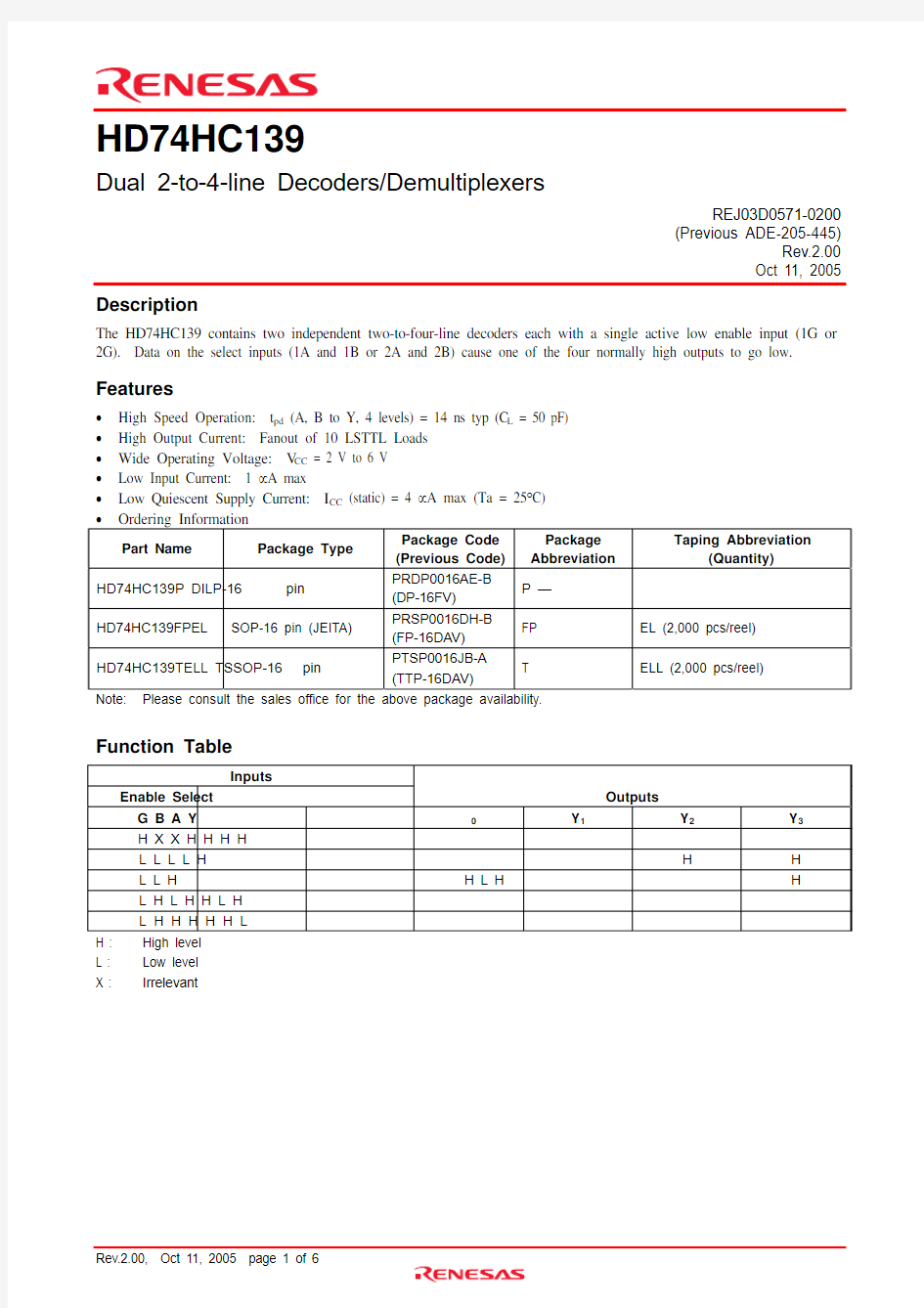
Function Table
Inputs
Enable Select Outputs
G B A Y0Y1Y2Y3
H X X H H H H
L L L L H H H L L H H L H H L H L H H L H L H H H H H L H : High level
L : Low level
X : Irrelevant
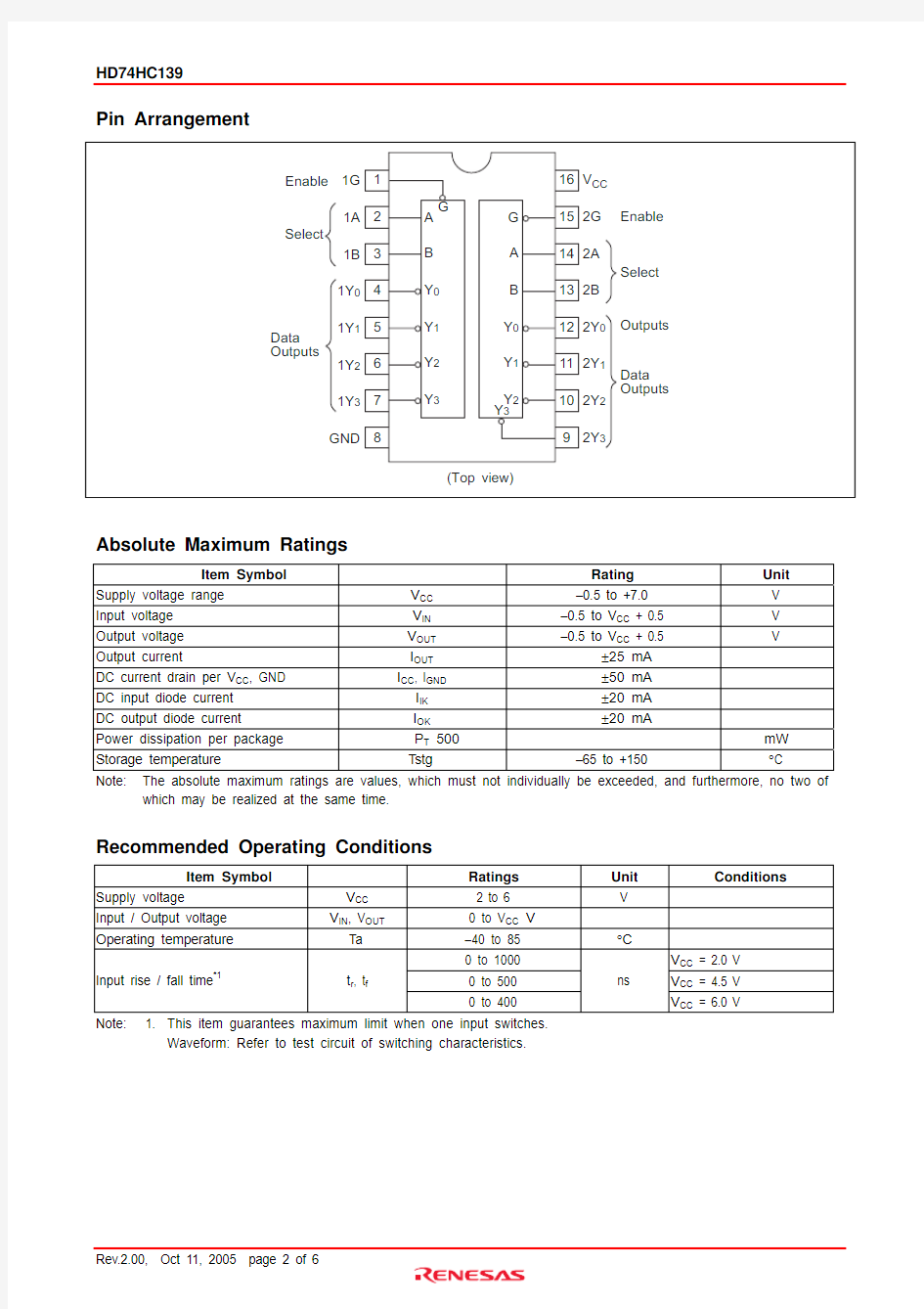
Pin Arrangement
Absolute Maximum Ratings
Item Symbol Rating Unit
Supply voltage range V CC –0.5 to +7.0 V Input voltage V IN –0.5 to V CC + 0.5 V Output voltage V OUT –0.5 to V CC + 0.5 V Output current I OUT ±25 mA DC current drain per V CC , GND I CC , I GND ±50 mA DC input diode current I IK ±20 mA DC output diode current I OK ±20 mA Power dissipation per package P T 500 mW Storage temperature Tstg –65 to +150 °C Note: The absolute maximum ratings are values, which must not individually be exceeded, and furthermore, no two of
which may be realized at the same time.
Recommended Operating Conditions
Item Symbol Ratings Unit Conditions
Supply voltage V CC 2 to 6 V Input / Output voltage V IN , V OUT 0 to V CC V Operating temperature Ta –40 to 85 °C 0 to 1000
V CC = 2.0 V 0 to 500
V CC = 4.5 V Input rise / fall time *1
t r , t f
0 to 400
ns
V CC = 6.0 V
Note: 1. This item guarantees maximum limit when one input switches. Waveform: Refer to test circuit of switching characteristics.
Electrical Characteristics
Ta = 25°C Ta = –40 to+85°C
Item Symbol V CC (V) Min Typ Max Min Max Unit
Test Conditions
2.0 1.5 — — 1.5 — 4.5
3.15 — — 3.15 — V IH
6.0 4.2 — — 4.2 —
V 2.0 — — 0.5 — 0.5 4.5 — — 1.35 — 1.35 Input voltage
V IL 6.0 — — 1.8 — 1.8
V
2.0 1.9 2.0 — 1.9 — 4.5 4.4 4.5 — 4.4 — 6.0 5.9 6.0 — 5.9 — I OH = –20 μA
4.5 4.18 — — 4.13 — I OH = –4 mA V OH 6.0
5.68 — — 5.63 — V Vin = V IH or V IL I OH = –5.2 mA
2.0 — 0.0 0.1 — 0.1 4.5 — 0.0 0.1 — 0.1 6.0 — 0.0 0.1 — 0.1 I OL = 20 μA
4.5 — — 0.26 — 0.33 I OL = 4 mA Output voltage
V OL 6.0 — — 0.26 — 0.33 V Vin = V IH or V IL I OL = 5.2 mA
Input current Iin 6.0 — — ±0.1 — ±1.0 μA Vin = V CC or GND
Quiescent supply
current I CC 6.0
— — 4.0 — 40 μA Vin = V CC or GND, Iout = 0 μA
Switching Characteristics (C L = 50 pF, Input t r = t f = 6 ns)
Ta = 25°C Ta = –40 to +85°C
Item Symbol V CC (V) Min Typ Max Min Max Unit
Test Conditions
2.0 — — 150 — 190 4.5 — 15 30 — 38 t PHL
6.0 — — 26 — 33 ns 2.0 — — 150 — 190 4.5 — 13 30 — 38 t PLH
6.0 — — 26 — 33 ns Select to any Y (4 levels) 2.0 — — 150 — 190 4.5 — 18 30 — 38 t PHL
6.0 — — 26 — 33 ns 2.0 — — 150 — 190 4.5 — 18 30 — 38 t PLH
6.0 — — 26 — 33 ns Select to any Y (5 levels) 2.0 — — 160 — 220 4.5 — 19 32 — 40 t PHL
6.0 — — 27 — 34 ns 2.0 — — 160 — 200 4.5 — 16 32 — 40 Propagation delay
time
t PLH
6.0 — — 27 — 34 ns Enable to any Y 2.0 — — 75 —
95 4.5 — 5 15 — 19 Output rise/fall
time
t TLH , t THL
6.0 — — 13 — 16 ns Input capacitance Cin
— — 5 10
—
10 pF
Test Circuit
Waveforms
Package Dimensions
https://www.doczj.com/doc/ac5144043.html, RENESAS SALES OFFICES
Refer to "https://www.doczj.com/doc/ac5144043.html,/en/network" for the latest and detailed information.
Renesas Technology America, Inc.
450 Holger Way, San Jose, CA 95134-1368, U.S.A
Tel: <1> (408) 382-7500, Fax: <1> (408) 382-7501
Renesas Technology Europe Limited
Dukes Meadow, Millboard Road, Bourne End, Buckinghamshire, SL8 5FH, U.K.
Tel: <44> (1628) 585-100, Fax: <44> (1628) 585-900
Renesas Technology (Shanghai) Co., Ltd.
Unit 205, AZIA Center, No.133 Yincheng Rd (n), Pudong District, Shanghai 200120, China
Tel: <86> (21) 5877-1818, Fax: <86> (21) 6887-7898
Renesas Technology Hong Kong Ltd.
7th Floor, North Tower, World Finance Centre, Harbour City, 1 Canton Road, Tsimshatsui, Kowloon, Hong Kong
Tel: <852> 2265-6688, Fax: <852> 2730-6071
Renesas Technology Taiwan Co., Ltd.
10th Floor, No.99, Fushing North Road, Taipei, Taiwan
Tel: <886> (2) 2715-2888, Fax: <886> (2) 2713-2999
Renesas Technology Singapore Pte. Ltd.
1 Harbour Front Avenue, #06-10, Keppel Bay Tower, Singapore 098632
Tel: <65> 6213-0200, Fax: <65> 6278-8001
Renesas Technology Korea Co., Ltd.
Kukje Center Bldg. 18th Fl., 191, 2-ka, Hangang-ro, Yongsan-ku, Seoul 140-702, Korea
Tel: <82> (2) 796-3115, Fax: <82> (2) 796-2145
Renesas Technology Malaysia Sdn. Bhd
Unit 906, Block B, Menara Amcorp, Amcorp Trade Centre, No.18, Jalan Persiaran Barat, 46050 Petaling Jaya, Selangor Darul Ehsan, Malaysia
Tel: <603> 7955-9390, Fax: <603> 7955-9510
? 2005. Renesas Technology Corp., All rights reserved. Printed in Japan.