FEATURES APPLICATIONS
DESCRIPTION
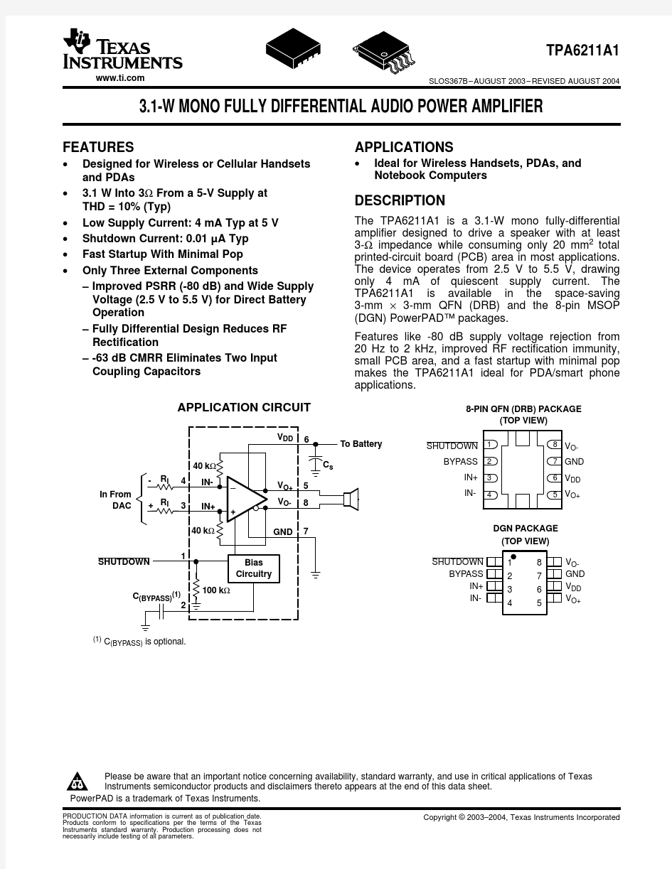
APPLICATION CIRCUIT
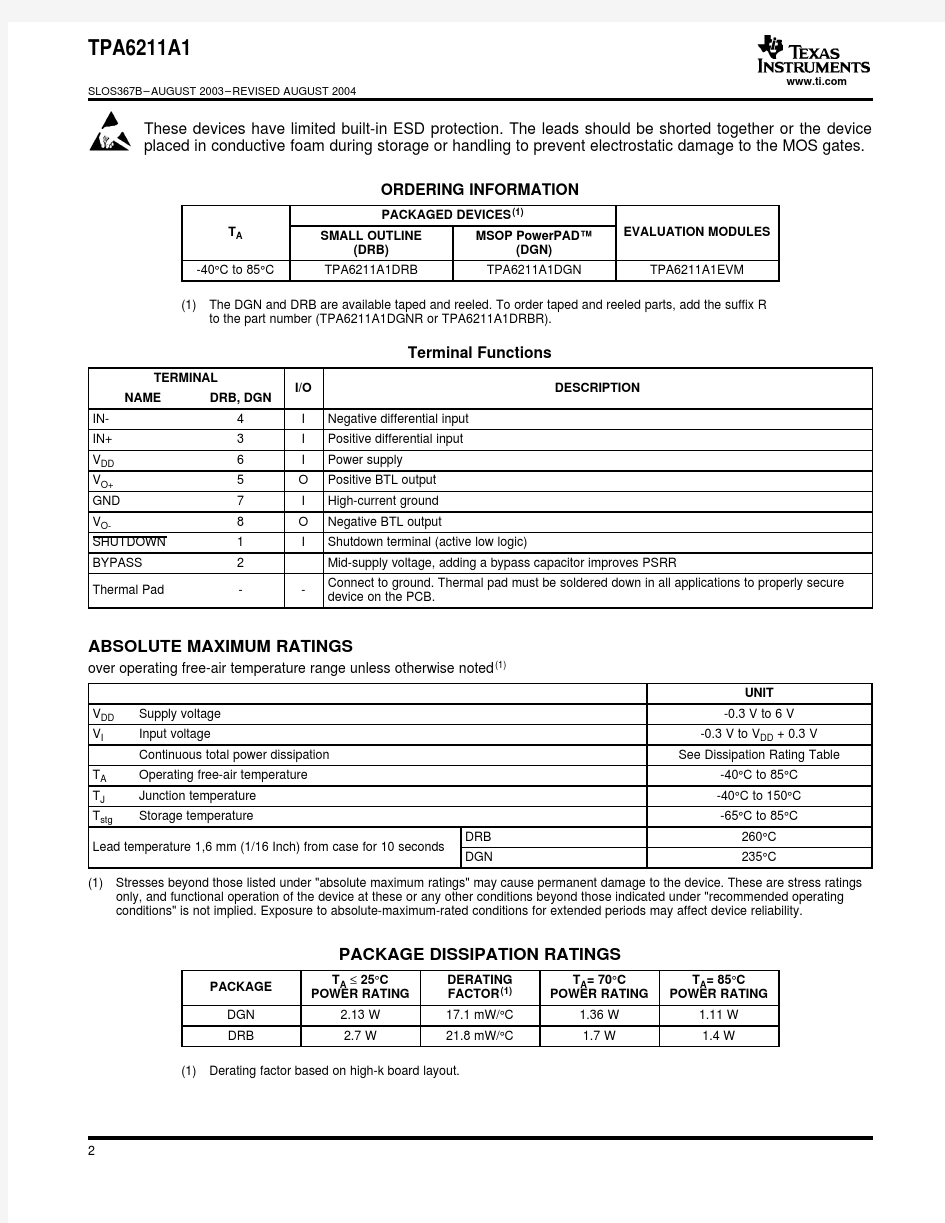
DGN PACKAGE
(TOP VIEW)
SHUTDOWN
BYPASS
IN+
IN-
V O-
GND
V DD
V O+
O-
DD
O+
8-PIN QFN (DRB) PACKAGE
(1) C(BYPASS) is optional.
TPA6211A1
SLOS367B–AUGUST2003–REVISED AUGUST2004
3.1-W MONO FULLY DIFFERENTIAL AUDIO POWER AMPLIFIER
?Ideal for Wireless Handsets,PDAs,and ?Designed for Wireless or Cellular Handsets
Notebook Computers
and PDAs
? 3.1W Into3?From a5-V Supply at
THD=10%(Typ)
The TPA6211A1is a 3.1-W mono fully-differential ?Low Supply Current:4mA Typ at5V
amplifier designed to drive a speaker with at least ?Shutdown Current:0.01μA Typ
3-?impedance while consuming only20mm2total ?Fast Startup With Minimal Pop printed-circuit board(PCB)area in most applications.
The device operates from2.5V to5.5V,drawing ?Only Three External Components
only4mA of quiescent supply current.The –Improved PSRR(-80dB)and Wide Supply
TPA6211A1is available in the space-saving Voltage(2.5V to5.5V)for Direct Battery
3-mm×3-mm QFN(DRB)and the8-pin MSOP Operation(DGN)PowerPAD?packages.
–Fully Differential Design Reduces RF
Features like-80dB supply voltage rejection from Rectification
20Hz to2kHz,improved RF rectification immunity,–-63dB CMRR Eliminates Two Input small PCB area,and a fast startup with minimal pop Coupling Capacitors makes the TPA6211A1ideal for PDA/smart phone
applications.
Please be aware that an important notice concerning availability,standard warranty,and use in critical applications of Texas
Instruments semiconductor products and disclaimers thereto appears at the end of this data sheet.
PowerPAD is a trademark of Texas Instruments.
https://www.doczj.com/doc/af4904436.html,
These devices have limited built-in ESD protection.The leads should be shorted together or the device placed in conductive foam during storage or handling to prevent electrostatic damage to the MOS gates.
ORDERING INFORMATION
(1)The DGN and DRB are available taped and reeled.To order taped and reeled parts,add the suffix R
to the part number(TPA6211A1DGNR or TPA6211A1DRBR).
Terminal Functions
over operating free-air temperature range unless otherwise noted(1)
(1)Stresses beyond those listed under"absolute maximum ratings"may cause permanent damage to the device.These are stress ratings
only,and functional operation of the device at these or any other conditions beyond those indicated under"recommended operating conditions"is not implied.Exposure to absolute-maximum-rated conditions for extended periods may affect device reliability.
(1)Derating factor based on high-k board layout.
https://www.doczj.com/doc/af4904436.html,
RECOMMENDED OPERATION CONDITIONS
ELECTRICAL CHARACTERISTICS
TPA6211A1
SLOS367B–AUGUST 2003–REVISED AUGUST 2004
T A =25°C
https://www.doczj.com/doc/af4904436.html,
OPERATING CHARACTERISTICS
TPA6211A1
SLOS367B–AUGUST 2003–REVISED AUGUST 2004
T A =25°C,Gain =1V/V
https://www.doczj.com/doc/af4904436.html,
TYPICAL CHARACTERISTICS
Table of Graphs
00.511.522.533.52.5
3
3.54
4.5
5
V DD - Supply Voltage - V
- O u t p u t P o w e r - W
P O
R L - Load Resistance - ?
- O u t p u t P o w e r - W
P O
3813182328
TPA6211A1
SLOS367B–AUGUST 2003–REVISED AUGUST 2004
OUTPUT POWER
OUTPUT POWER
vs
vs
SUPPLY VOLTAGE
LOAD RESISTANCE
Figure 1.Figure 2.
https://www.doczj.com/doc/af4904436.html,
P O - Output Power - W
- P o w e r D i s s i a p t i o n - W
P
D 0
0.2
0.40.60.811.21.4
P O - Output Power - W
- P o w e r D i s s i a p t i o n - W
P D 0.01
100.020.050.10.20.512
P O - Output Power - W
T H D +N - T o t a l H a r m o n i c D i s t o r t i o n + N o i s e - %
P O - Output Power - W
T H D +N - T o t a l H a r m o n i c D i s t o r t i o n + N o i s e - %
TPA6211A1
SLOS367B–AUGUST 2003–REVISED AUGUST 2004
POWER DISSIPATION
POWER DISSIPATION
vs
vs
OUTPUT POWER
OUTPUT POWER
Figure 3.
Figure 4.
TOTAL HARMONIC DISTORTION +NOISE
TOTAL HARMONIC DISTORTION +NOISE
vs
vs
OUTPUT POWER
OUTPUT POWER
Figure 5.Figure 6.
https://www.doczj.com/doc/af4904436.html,
f - Frequency - Hz
T H D +N - T o t a l H a r
m o n i c D i s t o r t i o n + N o i s e - %
P O - Output Power - W
T H D +N - T o t a l H a r m o n i c D i s t o r t i o n + N o i s e - %
f - Frequency - Hz
T H D +N - T o t a l H a r m o n i c D i s t o r t i o n + N o i s e - %
f - Frequency - Hz
T H D +N - T o t a l H a r m o n i c D i s t o r t i o n + N o i s e - %
TPA6211A1
SLOS367B–AUGUST 2003–REVISED AUGUST 2004
TOTAL HARMONIC DISTORTION +NOISE
TOTAL HARMONIC DISTORTION +NOISE
vs
vs
OUTPUT POWER
FREQUENCY
Figure 7.
Figure 8.
TOTAL HARMONIC DISTORTION +NOISE
TOTAL HARMONIC DISTORTION +NOISE
vs
vs
FREQUENCY
FREQUENCY
Figure 9.Figure 10.
https://www.doczj.com/doc/af4904436.html,
f - Frequency - Hz
T H D +N - T o t a l H a r m o n i c D i s t o r t i o n + N o i s e - %
f - Frequency - Hz
T H D +N - T o t a l H a r m o n i c D i s t o r t i o n + N o i s e - %
f - Frequency - Hz
k S V R - S u p p l y V o l t a g e R e j e c t i o n R a t i o - d B
12345
V IC - Common Mode Input Voltage - V
T H D +N - T o t a l H a r m o n i c D i s t o r t i o n + N o i s e - %
TPA6211A1
SLOS367B–AUGUST 2003–REVISED AUGUST 2004
TOTAL HARMONIC DISTORTION +NOISE
TOTAL HARMONIC DISTORTION +NOISE
vs
vs
FREQUENCY
FREQUENCY
Figure 11.
Figure 12.
TOTAL HARMONIC DISTORTION +NOISE
SUPPLY VOLTAGE REJECTION RATIO
vs
vs
COMMON MODE INPUT VOLTAGE
FREQUENCY
Figure 13.Figure 14.
https://www.doczj.com/doc/af4904436.html,
f - Frequency - Hz
k S V R - S u p p l y V o l t a g e R e j e c t i o n R a t i o - d B
f - Frequency - Hz
k S V R - S u p p l y V o l t a g e R e j e c t i o n R a t i o - d B
k S V R ? S u p p l y V o l t a g e R e j e c t i o n R a t i o ? d B
f ? Frequency ? Hz
DC Common Mode Input ? V
k S V R ? S u p p l y V o l t a g e R e j e c t i o n R a t i o ? d B
TPA6211A1
SLOS367B–AUGUST 2003–REVISED AUGUST 2004
SUPPLY VOLTAGE REJECTION RATIO
SUPPLY RIPPLE REJECTION RATIO
vs
vs
FREQUENCY
FREQUENCY
Figure 15.
Figure 16.
SUPPLY VOLTAGE REJECTION RATIO
SUPPLY VOLTAGE REJECTION RATIO
vs
vs
FREQUENCY
DC COMMON MODE INPUT
Figure 17.Figure 18.
https://www.doczj.com/doc/af4904436.html,
C1
Frequency 217 Hz C1 ? Duty 20%
C1 Pk?Pk 500 mV
Ch1 100 mV/div Ch4 10 mV/div
2 ms/div
V DD
V OUT
V o l t a g e ? V
t ? Time ? ms
R L = 8 ?
C I = 2.2 μF
C (BYPASS) = 0.47 μF
?150
?100
?50
f ? Frequency ? Hz
? S u p p l y V o l t a g e ? d B V V D D ? O u t p u t V o l t a g e ? d B V
V O TPA6211A1
SLOS367B–AUGUST 2003–REVISED AUGUST 2004
GSM POWER SUPPLY REJECTION
vs TIME
Figure 19.
GSM POWER SUPPLY REJECTION
vs
Figure 20.
https://www.doczj.com/doc/af4904436.html,
f - Frequency - Hz
C M R R - C o m m o n -M o d e R e j e c t i o n R a t i o - d B
-90
-80-70-60-50-40-30-20-10V IC - Common Mode Input Voltage - V
C M R R - C o m m o n M o d e R e j e c t i o n R a t i o - d B
-80
-70-60-50-40-30-20-10 f - Frequency - Hz
G a i n - d B
P h a s e - D e g r e e s
100
1 k
10 k 100 k
1 M
f ? Frequency ? Hz P h a s e ? D e
g r e e s G a i n ? d B
TPA6211A1
SLOS367B–AUGUST 2003–REVISED AUGUST 2004
COMMON MODE REJECTION RATIO
COMMON-MODE REJECTION RATIO
vs
vs
FREQUENCY
COMMON-MODE INPUT VOLTAGE
Figure 21.
Figure 22.
CLOSED LOOP GAIN/PHASE
OPEN LOOP GAIN/PHASE
vs
vs
FREQUENCY
FREQUENCY
Figure 23.Figure 24.
https://www.doczj.com/doc/af4904436.html,
0.51.52.53.54.5V DD - Supply Voltage - V
I D D - S u p p l y C u r r e n t - m
A
0.00001
0.0001
0.001
0.01
0.1
1
10
Voltage on SHUTDOWN Terminal - V
I D D - S u p p l y C u r r
e n t - m A
050
100
150
200
250300
0.20.40.60.81
C (Bypass) - Bypass Capacitor - μF
S t a r t -U p T i m e - m s
TPA6211A1
SLOS367B–AUGUST 2003–REVISED AUGUST 2004
SUPPLY CURRENT
SUPPLY CURRENT
vs
vs
SUPPLY VOLTAGE
SHUTDOWN VOLTAGE
Figure 25.
Figure 26.
START-UP TIME
vs
BYPASS CAPACITOR
Figure 27.
https://www.doczj.com/doc/af4904436.html,
APPLICATION INFORMATION
FULLY DIFFERENTIAL AMPLIFIER
Advantages of Fully Differential Amplifiers
APPLICATION SCHEMATICS
(1) C
(BYPASS) is optional
TPA6211A1
SLOS367B–AUGUST 2003–REVISED AUGUST 2004
?
Mid-supply bypass capacitor,C (BYPASS),not required:The fully differential amplifier does not require a bypass capacitor.Any shift in the The TPA6211A1is a fully differential amplifier with mid-supply voltage affects both positive and differential inputs and outputs.The fully differential negative channels equally,thus canceling at the amplifier consists of a differential amplifier and a differential output.Removing the bypass capaci-common-mode amplifier.The differential amplifier tor slightly worsens power supply rejection ratio ensures that the amplifier outputs a differential volt-(k SVR ),but a slight decrease of k SVR may be age that is equal to the differential input times the acceptable
when an additional component can be gain.The common-mode feedback ensures that the eliminated (See Figure 17).
common-mode voltage at the output is biased around ?
Better RF-immunity:GSM handsets save power V DD /2regardless of the common-mode voltage at the by turning on and shutting off the RF transmitter input.
at a rate of 217Hz.The transmitted signal is picked-up on input and output traces.The fully differential amplifier cancels the signal much ?Input coupling capacitors not required:A fully
better than the typical audio amplifier.
differential amplifier with good CMRR,like the TPA6211A1,allows the inputs to be biased at voltage other than mid-supply.For example,if a DAC has a lower mid-supply voltage than that of Figure 28through Figure 31show application sche-the TPA6211A1,the common-mode feedback matics for differential and single-ended inputs.Typical circuit compensates,and the outputs are still values are shown in Table 1.
biased at the mid-supply point of the TPA6211A1.The inputs of the TPA6211A1can be biased from Table 1.Typical Component Values
0.5V to V DD -0.8V.If the inputs are biased outside of that range,input coupling capacitors are required.
(1)
C (BYPASS)is optional.
Figure 28.Typical Differential Input Application Schematic
https://www.doczj.com/doc/af4904436.html,
(1) C
(BYPASS) is optional
(1) C
(BYPASS) is optional
TPA6211A1
SLOS367B–AUGUST 2003–REVISED AUGUST 2004
Figure 29.Differential Input Application Schematic Optimized With Input Capacitors
Figure 30.Single-Ended Input Application Schematic
https://www.doczj.com/doc/af4904436.html,
+
?
(1) C(BYPASS) is optional Selecting Components
Gain = R F/R I(1)
f c+1
2p R
I C I
(2)
-3 dB
f c TPA6211A1
SLOS367B–AUGUST2003–REVISED AUGUST2004
Figure31.Differential Input Application Schematic With Input Bandpass Filter
Input Capacitor(C I)
The TPA6211A1does not require input coupling Resistors(R I)capacitors when driven by a differential input source
biased from0.5V to V https://www.doczj.com/doc/af4904436.html,e1%tolerance The input resistor(R I)can be selected to set the gain
or better gain-setting resistors if not using input of the amplifier according to equation1.
coupling capacitors.
In the single-ended input application,an input capaci-
The internal feedback resistors(R F)are trimmed to tor,C
I ,is required to allow the amplifier to bias the
40k?.input signal to the proper dc level.In this case,C
I and
R I form a high-pass filter with the corner frequency Resistor matching is very important in fully differential
defined in Equation2.
amplifiers.The balance of the output on the reference
voltage depends on matched ratios of the resistors.
CMRR,PSRR,and the cancellation of the second
harmonic distortion diminishes if resistor mismatch
occurs.Therefore,1%-tolerance resistors or better
are recommended to optimize performance.
Bypass Capacitor(C BYPASS)and Start-Up Time
The internal voltage divider at the BYPASS pin of this
device sets a mid-supply voltage for internal refer-
ences and sets the output common mode voltage to
V DD/2.Adding a capacitor filters any noise into this
pin,increasing k SVR.C(BYPASS)also determines the rise
time of V O+and V O-when the device exits shutdown.
The larger the capacitor,the slower the rise time.
https://www.doczj.com/doc/af4904436.html,
f c(HPF)+
12p 10k W C
I (8)
C I +
12p 10k W f
c(HPF)
(9)
C I +
12p R I f c
(3)f c(LPF)
+
12p R a C a
(10)
C a +
1
2p 1k ?f
c(LPF)
(11)
f c(LPF)+
12p R F C
F
where R F
is the internal 40k W resistor
(4)f c(LPF)+
12p 40k W C
F
(5)
C F +
1
2p 40k W f
c(LPF)
(6)
c(HPF)+20 dB/dec
f
c(LPF)f
c(HPF)+
1
2p R I C
I
where R I is the input resistor
(7)
TPA6211A1
SLOS367B–AUGUST 2003–REVISED AUGUST 2004
The value of C I is an important consideration.It Substituting R I into equation 6.
directly affects the bass (low frequency)performance of the circuit.Consider the example where R I is 10k ?and the specification calls for a flat bass response down to 100Hz.Equation 2is reconfigured as Therefore,
Equation 3.
Substituting 100Hz for f c(HPF)and solving for C I :In this example,C I is 0.16μF,so the likely choice
C I =0.16μF
ranges from 0.22μF to 0.47μF.Ceramic capacitors are preferred because they are the best choice in At this point,a first-order band-pass filter has been
preventing leakage current.When polarized capaci-created with the low-frequency cutoff set to 100Hz tors are used,the positive side of the capacitor faces and the high-frequency cutoff set to 10kHz.
the amplifier input in most applications.The input dc level is held at V DD /2,typically higher than the source The process can be taken a step further by creating a dc level.It is important to confirm the capacitor second-order high-pass filter.This is accomplished by polarity in the application.
placing a resistor (R a )and capacitor (C a )in the input path.It is important to note that R a must be at least Band-Pass Filter (R a ,C a ,and C a )
10times smaller than R I ;otherwise its value has a noticeable effect on the gain,as R a and R I are in It may be desirable to have signal filtering beyond the series.
one-pole high-pass filter formed by the combination of C I and R I .A low-pass filter may be added by placing Step 3:Additional Low-Pass Filter
a capacitor (C F )between the inputs and outputs,R a must be at least 10x smaller than
R I ,
forming a band-pass filter.
Set R a =1k ?
An example of when this technique might be used would be in an application where the desirable pass-band range is between 100Hz and 10kHz,with a gain of 4V/V.The following equations illustrate how Therefore,
the proper values of C F and C I can be determined.
Step 1:Low-Pass Filter
Substituting 10kHz for f c(LPF)and solving for C a :
C a =160pF
Figure 32is a bode plot for the band-pass filter in the previous example.Figure 31shows how to configure the TPA6211A1as a band-pass filter.
Therefore,
Substituting 10kHz for f c(LPF)and solving for C F :C F =398pF
Step 2:High-Pass Filter
Figure 32.Bode Plot
Since the application in this case requires a gain of 4V/V,R I must be set to 10k ?.
https://www.doczj.com/doc/af4904436.html,
V (rms)+
V
O(PP)22
?Power +
V
(rms)2R L
(12)
USING LOW-ESR
CAPACITORS
2x V
O(PP)
V
O(PP)
-V O(PP)
DIFFERENTIAL OUTPUT VERSUS f c +
12p R L C
C (13)TPA6211A1
SLOS367B–AUGUST 2003–REVISED AUGUST 2004
Decoupling Capacitor (C S )
The TPA6211A1is a high-performance CMOS audio amplifier that requires adequate power supply de-coupling to ensure the output total harmonic distortion (THD)is as low as possible.Power-supply decoupling also prevents oscillations for long lead lengths be-tween the amplifier and the speaker.For higher frequency transients,spikes,or digital hash on the line,a good low equivalent-series-resistance (ESR)ceramic capacitor,typically 0.1μF to 1μF,placed as close as possible to the device V DD lead works best.For filtering lower frequency noise signals,a 10-μF or greater capacitor placed near the audio power ampli-fier also helps,but is not required in most applications because of the high PSRR of this device.
Low-ESR capacitors are recommended throughout this applications section.A real (as opposed to ideal)capacitor can be modeled simply as a resistor in series with an ideal capacitor.The voltage drop across this resistor minimizes the beneficial effects of the capacitor in the circuit.The lower the equivalent Figure 33.Differential Output Configuration value of this resistance the more the real capacitor behaves like an ideal capacitor.
In a typical wireless handset operating at 3.6V,bridging raises the power into an 8-?speaker from a singled-ended (SE,ground reference)limit of 200SINGLE-ENDED OUTPUT
mW to 800mW.This is a 6-dB improvement in sound Figure 33shows a Class-AB audio power amplifier power—loudness that can be heard.In addition to (APA)in a fully differential configuration.The increased power,there are frequency-response con-TPA6211A1amplifier has differential outputs driving cerns.Consider the single-supply SE configuration both ends of the load.One of several potential shown in Figure 34.A coupling capacitor (C C )is benefits to this configuration is power to the load.The required to block the dc-offset voltage from the load.differential drive to the speaker means that as one This capacitor can be quite large (approximately 33side is slewing up,the other side is slewing down,μF to 1000μF)so it tends to be expensive,heavy,and vice versa.This in effect doubles the voltage occupy valuable PCB area,and have the additional swing on the load as compared to a drawback of limiting low-frequency performance.This ground-referenced load.Plugging 2×V O(PP)into the frequency-limiting effect is due to the high-pass filter power equation,where voltage is squared,yields 4×network created with the speaker impedance and the the output power from the same supply rail and load coupling capacitance.This is calculated with impedance Equation 12.
Equation 13.
For example,a 68-μF capacitor with an 8-?speaker
would attenuate low frequencies below 293Hz.The BTL configuration cancels the dc offsets,which elim-inates the need for the blocking capacitors.Low-frequency performance is then limited only by the input network and speaker response.Cost and PCB space are also minimized by eliminating the bulky coupling capacitor.
https://www.doczj.com/doc/af4904436.html,
V O(PP)
-3 dB
f
c
V(LRMS)
V
I DD(avg) FULLY DIFFERENTIAL AMPLIFIER
TPA6211A1
SLOS367B–AUGUST2003–REVISED AUGUST2004
An easy-to-use equation to calculate efficiency starts
out as being equal to the ratio of power from the
power supply to the power delivered to the load.To
accurately calculate the RMS and average values of
power in the load and in the amplifier,the current and
voltage waveform shapes must first be understood
(see Figure35).
Figure34.Single-Ended Output and Frequency
Response
Figure35.Voltage and Current Waveforms for Increasing power to the load does carry a penalty of BTL Amplifiers
increased internal power dissipation.The increased
dissipation is understandable considering that the
Although the voltages and currents for SE and BTL BTL configuration produces4×the output power of
are sinusoidal in the load,currents from the supply the SE configuration.
are different between SE and BTL configurations.In
an SE application the current waveform is a
half-wave rectified shape,whereas in BTL it is a EFFICIENCY AND THERMAL INFORMATION full-wave rectified waveform.This means RMS con-
version factors are different.Keep in mind that for Class-AB amplifiers are inefficient,primarily because
most of the waveform both the push and pull transis-of voltage drop across the output-stage transistors.
tors are not on at the same time,which supports the The two components of this internal voltage drop are
fact that each amplifier in the BTL device only draws the headroom or dc voltage drop that varies inversely
current from the supply for half the waveform.The to output power,and the sinewave nature of the
following equations are the basis for calculating output.The total voltage drop can be calculated by
amplifier efficiency.
subtracting the RMS value of the output voltage from
V DD.The internal voltage drop multiplied by the
average value of the supply current,I DD(avg),deter-
mines the internal power dissipation of the amplifier.
https://www.doczj.com/doc/af4904436.html,
Efficiency of a BTL amplifier +P L
P
SUP
Where:
P L +V L rms 2R L ,and V LRMS +V P 2?,therefore,P L +V P
2
2R
L
P L = Power delivered to load
P SUP = Power drawn from power supply V LRMS = RMS voltage on BTL load R L = Load resistance
V P = Peak voltage on BTL load
I DD avg = Average current drawn from the power supply V DD = Power supply voltage
ηBTL = Efficiency of a BTL amplifier
and P SUP +V DD I DD avg and I DD avg +1
p ?
p 0V
P R L
sin(t)dt +*1p V P R L [cos(t)]p 0+
2V P p R L Therefore,
P SUP +
2V
DD V
P p R
L
substituting P L and P SUP into equation 6,
Efficiency of a BTL amplifier +V P 2
2R L 2V DD V P p R L
+
p V P 4V DD
V
P
+
2P L R L
?Where:
h BTL +
p
2P L R L
?4V
DD
Therefore,
(15)
TPA6211A1
SLOS367B–AUGUST 2003–REVISED AUGUST 2004
(14)
Table 2.Efficiency and Maximum Ambient Temperature vs Output Power
(1)DRB package
(2)
Package limited to 85°C ambient
https://www.doczj.com/doc/af4904436.html,
θJA+1
Derating Factor +1
0.0218
+45.9°CńW
(17)
T A Max+T J Max*θJA P Dmax
+150*45.9(1.27)+91.7°C(18)
P Dmax+2V2
DD
p2R L
(16)
TPA6211A1
SLOS367B–AUGUST2003–REVISED AUGUST2004
Table2employs Equation15to calculate efficiencies
The maximum ambient temperature depends on the for four different output power levels.Note that the
heat sinking ability of the PCB system.The derating efficiency of the amplifier is quite low for lower power
factor for the3mm x3mm DRB package is shown in levels and rises sharply as power to the load is
the dissipation rating table.Converting this toθJA: increased resulting in a nearly flat internal power
dissipation over the normal operating range.Note that
the internal dissipation at full output power is less
than in the half power range.Calculating the ef-
GivenθJA,the maximum allowable junction tempera-ficiency for a specific system is the key to proper
ture,and the maximum internal dissipation,the maxi-power supply design.For a2.8-W audio system with
mum ambient temperature can be calculated with 4-?loads and a5-V supply,the maximum draw on
Equation18.The maximum recommended junction the power supply is almost3.8W.
temperature for the TPA6211A1is150°C.
A final point to remember about Class-A
B amplifiers
is how to manipulate the terms in the efficiency
equation to the utmost advantage when possible.
Note that in Equation15,V DD is in the denominator.
Equation18shows that the maximum ambient tem-This indicates that as V DD goes down,efficiency goes
perature is91.7°C(package limited to85°C ambient) up.
at maximum power dissipation with a5-V supply.
A simple formula for calculating the maximum power
Table2shows that for most applications no airflow is dissipated,P Dmax,may be used for a differential
required to keep junction temperatures in the speci-output application:
fied range.The TPA6211A1is designed with thermal
protection that turns the device off when the junction
temperature surpasses150°C to prevent damage to
the IC.In addition,using speakers with an impedance
higher than4-?dramatically increases the thermal P Dmax for a5-V,4-?system is1.27W.
performance by reducing the output current.