
P r e l i m i n a r y
U N G E N C O N F I D E N T I A L
SYNCHRONOUS DRAM MODULE
128M Bytes (32M x 32 bits)
PC133 SDRAM Unbuffered 100 Pin DIMM
based on 8 pcs 16M x 8 SDRAM with LVTTL, 4 banks & 4K Refresh
FEATURES
ABSOLUTE MAXIMUM RATINGS
REVISION HISTORY
Rev - A Product brief released.
Sept 27 , 2001
? Voltage Relative to GND -0.3 to + 4.6V ? Operating Temperature 0 to + 70°C ? Storage Temperature -55°C to + 125°C ? Short circuit Output Current 50mA ? Power Dissipation 8W
UG832T3248JSG-PL INTERNAL BANK REF. SDRAM PACKAGE PLATING
4 Banks
4K
TSOP
Gold
PART NO.
PART IDENTIFICATION
Single 3.3V ± 10% power supply
Utilizes 133 MHz CL3 SDRAM components Burst Mode Operation
Data scramble (Sequential & Interleave)All inputs are sampled at the positive going edge of the system clock Two Clocks System
Auto & self refresh capability (4096 Cycles/64ms)LVTTL compatible inputs and output Serial PD with EEPROM
PCB:Height (1250mil),double sided component
????????
? The UG832T3248JSG-PL is a 32Mbits x 32 Sync DRAM module. The UG832T3248JSG-PL is assembled using 8 pcs of 16M x 8 with 4 Banks Sync DRAMs in 54 pin TSOP packages mounted on 100 pin unbuffered printed circuit board.
GENERAL DESCRIPTION
?
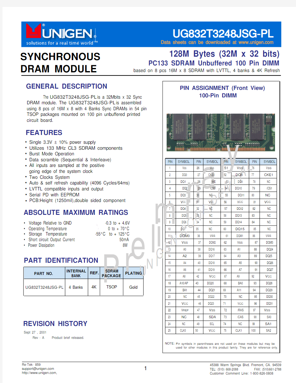
1 V SS 26 V SS 51 V SS 76 V SS
2 DQ0 27 CKE0 52 DQ8 77 CKE1
3 DQ1 28 /WE 53 DQ9 78 NC
4 DQ2 29 /CS0 54 DQ10 79 /CS1
5 DQ3 30 NC 55 DQ11 80 NC
6 V CC 31 V CC 56 V CC 81 V CC
7 DQ4 32 NC 57 DQ12 82 NC
8 DQ5 33 NC 58 DQ13 83 NC
9 DQ6 34 NC 59 DQ14 84 NC
10 DQ7 35 NC 60 DQ15 85 NC 11 DQM0 36 V SS 61 DQM1 86 V SS 12 V SS 37 DQM2 62 V SS 87 DQM313 A0 38 DQ16 63 A1 88 DQ24PIN SYMBOL PIN SYMBOL PIN SYMBOL PIN SYMBOL
l i C O N F I T I A L
Functional Block Diagram
Physical Dimension
V DD Vss
Two 0.33uF per each SDRAM
To all SDRAMs
A0 ~ A11, BA0 & BA1
CKE0
RAS CAS WE
SDRAM U0 ~ U7SDRAM U0 ~ U7SDRAM U0 ~ U7SDRAM U0 ~ U7SDRAM U0 ~ U3CKE1
SDRAM U4 ~ U7
Capacitors Serial PD
SDA
SCL
A1A2
A0SA1SA2
SA0U0 / U1U4 / U5
10W
10W
CLK0/1
U2 / U3U6 / U7
Note : ALL RESISTOR VALUES ARE 10 OHMS
0.050
0.150Max
0.050±0.0039
Detail C
0.250
Detail A
0.250
Detail B
0.200 M i n
( Front view )
( Back view )
Tolerances : ± 0.005 unless otherwise specified Units : Inches